Superstrong encapsulated monolayer graphene by the modified anodic bonding†
Wonsuk
Jung‡
a,
Taeshik
Yoon‡
a,
Jongho
Choi
b,
Soohyun
Kim
a,
Yong Hyup
Kim
*b,
Taek-Soo
Kim
*a and
Chang-Soo
Han
*c
aDepartment of Mechanical Engineering, KAIST, Daejeon, 305-701, Republic of Korea. E-mail: tskim1@kaist.ac.kr
bSchool of Mechanical and Aerospace Engineering, Seoul National University, Gwanak, Seoul 151-744, Republic of Korea. E-mail: yongkim@snu.ac.kr
cSchool of Mechanical Engineering, Korea University, Anam, Seongbuk, Seoul 136-701, Republic of Korea. E-mail: cshan@korea.ac.kr
First published on 17th October 2013
Abstract
We report a superstrong adhesive of monolayer graphene by modified anodic bonding. In this bonding, graphene plays the role of a superstrong and ultra-thin adhesive between SiO2 and glass substrates. As a result, monolayer graphene presented a strong adhesion energy of 1.4 J m−2 about 310% that of van der Waals bonding (0.45 J m−2) to SiO2 and glass substrates. This flexible solid state graphene adhesive can tremendously decrease the adhesive thickness from about several tens of μm to 0.34 nm for epoxy or glue at the desired bonding area. As plausible causes of this superstrong adhesion, we suggest conformal contact with the rough surface of substrates and generation of C–O chemical bonding between graphene and the substrate due to the bonding process, and characterized these properties using optical microscopy, atomic force microscopy, Raman spectroscopy, and X-ray photoelectron spectroscopy.
Introduction
The adhesion of graphene to various substrates has not been well researched even though it is used extensively in industrial applications, such as electronic packaging devices, flexible displays, and NEMS devices that require strong adhesion energy between graphene and the target substrate.1–9 A recent study reported an exfoliated monolayer graphene membrane attached to a SiO2 substrate displaying a 0.45 J m−2 adhesion energy.1 This high adhesion energy was attributed to the extreme flexibility of graphene, which made its interaction with the substrate liquid-like in nature. This liquid-like property of graphene maximizes the van der Waals forces between the graphene and substrate in the nanoscale regime.1,3–5 Recent studies measured the adhesion energy of graphene on a corrugated SiO2 substrate and nanoparticles with atomic force microscopy (AFM), obtaining values of 0.07 J m−2 and 0.15–0.3 J m−2, respectively.2,3,5 In addition, the adhesion energy of monolayer graphene grown on a Cu film was directly measured over a large area using the double cantilever beam (DCB) fracture mechanics test, obtaining a value of 0.72 J m−2.6However, natural contact between graphene and the substrate hardly ensures control over the adhesion energy and durability in several applications. Strong adhesion of graphene is required to avoid problems with delamination, reliability, vapor permeation, and other factors.7,9–11 Graphene can be easily detached from substrates by wet chemical processes to produce graphene FETs or nanoribbons.9 In addition, delamination of graphene from the substrate degenerates the charging and discharging ability of graphene fuel cells.10,11 Moreover, weakly bonded graphene can also be wrinkled and folded over long exposures to high humidity.7 In order to reinforce and control the graphene adhesion, conventional bonding methods can be considered but have not been tried yet.6,12–14 For example, bonding through an adhesive interlayer, such as glue or epoxy, may be the simplest process to adhere graphene to the target substrate.15 However, this method produces a thick adhesive layer in the range of tens of micrometers that is nonuniform in height, which can be subject to parasitic effects from the substrate, and inefficiently transfers heat with a coefficient of approximately 2–5 W m−1 K−1. The second approach is a non-epoxy bonding method, such as high temperature bonding,14 plasma bonding,12 and eutectic or thermo-composition bonding using a metal interlayer.13 However, these methods require high temperatures of up to 1000 °C, O2 plasma treatment, and the addition of metal materials to an interlayer at high pressures, which could seriously damage graphene. Therefore, enhancing the bonding force of graphene to substrates is of significance to many applications. Moreover, the use of graphene as an adhesive between two substrates has not yet been exploited.
In this paper, we explore a new role of monolayer graphene in anodic bonding as an adhesive between SiO2 and glass substrates. Anodic bonding has been widely used in the Si industry16 and in a broad range of other fields.17 This bonding method has been used for bonding glass substrates to target materials,18 such as Si, metals (Alloy 42, Invar, Kovar, Ni),19 and oxide materials (SiO2). The principle of anodic bonding is based on the conductive solid electrolyte state of glass over 250 °C that has an alkali composition containing Na2O or K2O (for example, Pyrex 7740 from Corning or Boro 33 from i-Nexus) and high electrostatic forces that result in an ion depletion layer at the bonding interface under applied voltage, typically on the order of several kilovolts across the bonding substrates.20 The cathode and anode are conventionally connected to the surfaces of glass and Si substrates to generate high potential voltage, inducing migration of Na+ and K+ ions that were already decomposed from Na2O and K2O at the high temperature. The decomposed alkali ions, such as Na+ and K+, have higher mobility than O2− ions; therefore, they migrate to the cathode plate connected to the glass substrate. The remaining O2− ions generate high electrostatic forces at the interface between the glass and counter substrate.18 The counter substrate, typically a Si wafer, does not decompose into ions; instead, it retains its original composition, except at the bonding interface. The strong electric field at the interface pulls the wafer into intimate contact with the substrate, ultimately leading to the formation of stable Si–O–Si bonds and resulting in a strong bonding of the wafer to the glass substrate.18 Recently, electrostatic forces induced by high voltages were used to exfoliate graphene from highly oriented pyrolytic graphite (HOPG).18,21–23 Instead of using a Si substrate in the anodic bonding process, HOPG was used as a positive electrode and a glass substrate was used as a negative electrode.18,21,22 Additionally, a SiO2 substrate was adopted as a negative electrode to transfer graphene from graphite to SiO2 by anodic bonding.23 However, this method is imperfect because it can only exfoliate local areas of graphene.
Results and discussion
Monolayer graphene adhesive for modified anodic bonding
In this paper, we describe an anodic bonding process using monolayer graphene between SiO2 and glass substrates at high electrostatic forces and temperatures over 250 °C. Monolayer graphene was grown on copper foil by CVD (see Methods) and transferred to large areas of SiO2/Si substrates (5 mm in width and 35 mm in length) for direct measurement of adhesion energy via the DCB fracture mechanics test (see ESI†). Graphene is transferred by a wet method using polymethyl methacrylate (PMMA) and a copper etchant. A 50 nm thick SiO2 layer was deposited onto a polished Si substrate by thermal oxidation at 1000 °C to obtain a very flat surface with a roughness of less than 1 nm rms. The relatively thin SiO2 substrate compared to a typical SiO2 wafer of 300 nm reinforced the electrostatic force at the bonding interface. The newly suggested bonding method is illustrated in Fig. 1a. The transferred graphene conformed to the topography of the SiO2 substrate, even in locations where the surface was not very flat.1 The transferred graphene was aligned with the glass substrate of the same size containing Na2O and K2O. Heat and pressure, approximately 12.5 N cm−2, were applied to the samples under a vacuum of 50 mTorr. Voltages of 800 and 950 V were applied across the samples for 15 min at temperatures of 280 and 380 °C, with the cathode and anode connected to the top of the glass and the bottom of the Si substrate, respectively. The applied voltage was distributed across the interface region of the Pyrex glass and the SiO2 layer on the Si wafer. The electrostatic field distributed across the SiO2 (50 nm) and O2− (about 30 nm) depletion region was approximately 11.9 V nm−1. After this modified anodic bonding process, the SiO2/Si and glass substrates were strongly bonded to the monolayer graphene. We investigated experimental parameters such as temperature and voltage. High temperature increases the mobility and diffusion of ions in the glass in its conductive solid electrolyte state. Additionally, increasing the applied voltage increases the decomposition and drift velocity of ions. However, extremely high temperatures of over 400 °C under low vacuum conditions at high voltages of over 1200 V can destroy the graphene structures and generate defects. Therefore, we investigated the bonding quality under four conditions, 380 °C, 950 V (C1), 380 °C, 800 V (C2), 280 °C, 950 V (C3), and 280 °C, 800 V (C4) and an additional control experiment without external voltage under identical temperature conditions. We then estimated the bonding quality in terms of adhesion energy and uniformity of bonding.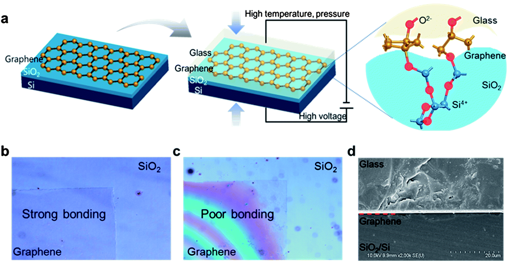 | ||
| Fig. 1 Modified anodic bonding using monolayer graphene adhesive: (a) schematic description of the newly suggested bonding method. Graphene transferred to the SiO2 substrate is a flexible adhesive between glass and SiO2 at a high temperature and voltage environment. (b) The case of strong bonding shows the transparent graphene area on the SiO2. (c) On the other hand, if the sample is not bonded or has low bonding energy, there is a Newton's ring at the graphene area, as seen in the right image. (d) This cross-sectional image shows the composition of the sample and flexible interaction of graphene between the glass and SiO2/Si. | ||
Bonding uniformity was investigated by void observation, as presented in Fig. 1b and c. In the case of strong bonding, there was a transparent graphene area on the SiO2 because of the absence of voids (Fig. 1b). The graphene area is darker in color because monolayer graphene has a maximum transparency of approximately 97.7% under white light.24 On the other hand, if the sample is not bonded in the control experiment or has low bonding energy, Newton's rings are formed due to the effect of light interference, as shown in Fig. 1c and S4.† Moreover, these unbonded samples are easily detached from each other. The conformal close contact between graphene and the substrate can be observed in cross-sectional images of the SiO2/Si, graphene, and glass layers (Fig. 1d). Even though there are some ripples of transferred graphene, the space charging of the depletion layer, which generates strong interfacial electrostatic attractive forces, induces conformal contact of graphene to the substrate.
Direct measurement of adhesion energy using DCB fracture mechanics test
Indirect methods have been proposed to measure graphene adhesion. However, these methods are limited to local areas and are not appropriate for estimating large areas of graphene. We used DCB fracture mechanics testing to measure the adhesion energy. The geometry of the DCB specimen caused a pure mode I fracture. Therefore, the graphene over the specimen directly delaminated under tensile loading. We used beams composed of Si and glass. However, the beams had different Young's modulus values, resulting in asymmetric deformation of the beams. We chose the appropriate thickness for the Si and glass substrates by calculating the bending stiffness, thus ensuring symmetric beam deformation during the test. We also modified the analytical model of the DCB test, as presented in the ESI.† A pre-notch region was defined on the Si beam by 50 μm etching using a deep reactive ion etching (DRIE) process to obtain an unbonded region, as shown in Fig. 2a. After the two beams underwent anodic bonding, the loading grips were attached to pull the specimen onto the micromechanical test system (Delaminator Adhesion Test System, DTS Company). Fig. 2b presents the procedures for the DCB test. The load increased linearly once the specimen was loaded, as shown in the insets of Fig. 2b. A crack began to propagate when the applied loading was sufficiently high to overcome the adhesion energy of the surface. The critical load was defined as the point at which the load decreased. After the load decreased below a certain point, the motion was reversed to seize the crack. These procedures were repeated multiple times to measure the adhesion energy.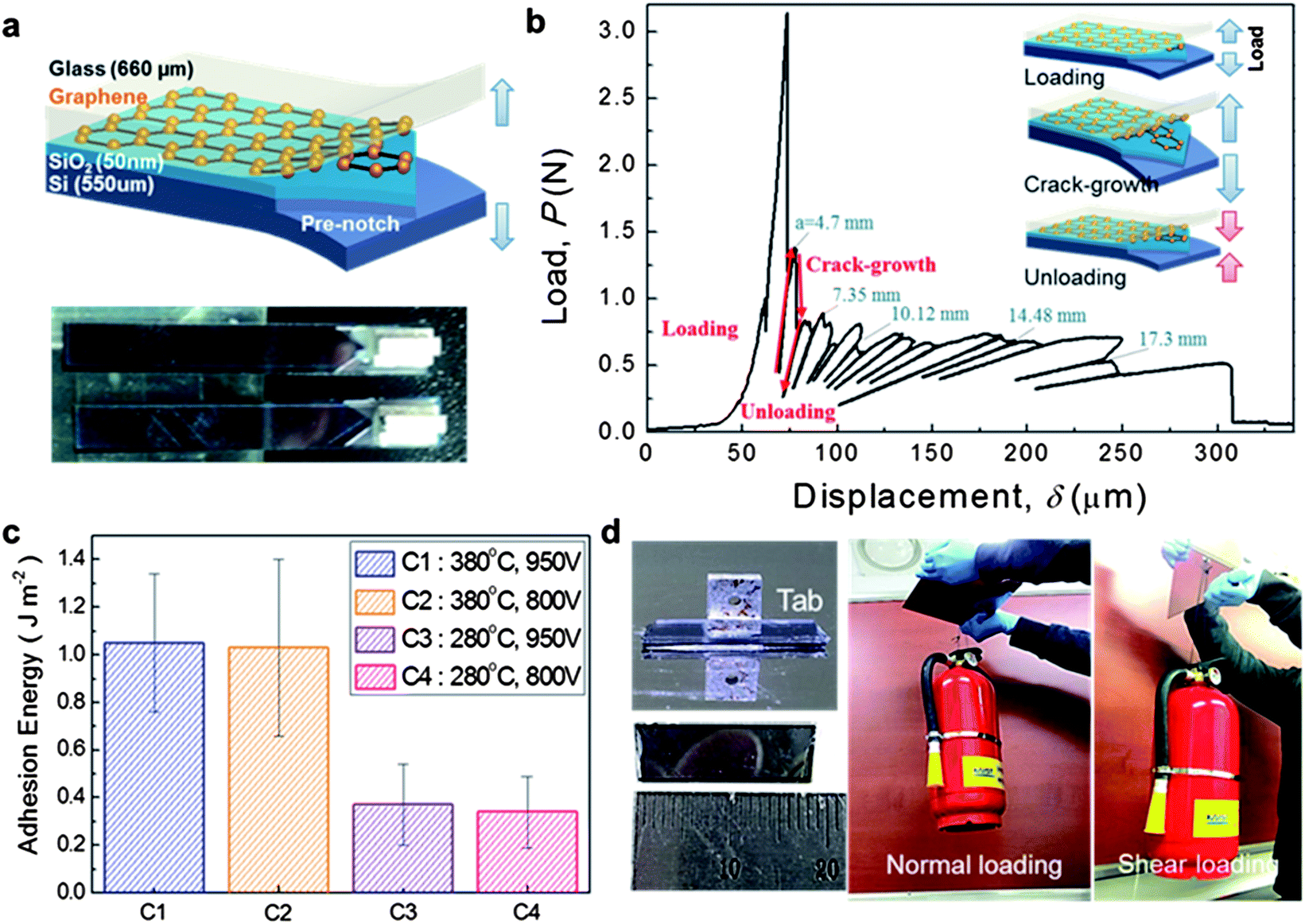 | ||
| Fig. 2 Adhesion energy measurement of bonded graphene using the DCB test: (a) the top is a schematic illustration of the DCB specimen and the bottom is an optical image of the specimen. The pre-notch region is defined by silicon etching to ensure crack initiation. (b) The conceptual illustrations of loading/crack-growth/unloading procedures of the DCB test are expressed in inset pictures. These procedures are repeated multiple times until the crack-tip meets the end of the specimen for measuring the crack lengths and adhesion energy of graphene. Some of the measured crack lengths, a, for each DCB cycle are shown. (c) The measured adhesion energy of bonded graphene at each temperature and voltage conditions. Temperature is the dominant factor for anodic bonding of graphene. (d) Demonstration of the adhesion energy of graphene adhesive by suspending a fire extinguisher. The specimen that has a bonded area of 0.8 cm2 (4.5 mm width and 18 mm length) sustains the calculated stress of 0.65 MPa. These experiments were carried out by suspending the object in a steady state environment and several accelerated motions (max 12.1 s−2). | ||
The crack length was calculated from the slopes of the curves. The adhesion energy was calculated from the corresponding crack length and critical load of each cycle. We observed that the cracks were more likely to propagate in the glass beam than at the interface when the speed was high. To prevent propagation in the glass beam, the test speed was fixed at 0.5 μm s−1. Some of the crack lengths are depicted in Fig. 2b. The measured adhesion energy for each condition is plotted in Fig. 2c. From these results, the highest and lowest adhesion energies were obtained for C1 and C4, respectively. The dominant factor for adhesion was temperature. The adhesion energy was 0.4 J m−2 at 280 °C, whereas it increased by approximately three-fold at 380 °C. Graphene adhesion is tunable and its adhesion could be increased to a maximum of 1.4 J m−2 and an average value of approximately 1.05 J m−2 at 380 °C by modifying the anodic bonding. The adhesion energy of graphene was higher under the conditions in this study than for the original anodic bonding conditions used for Si and glass wafers, which displayed lower adhesion energies of 0.4–1.25 J m−2 at 300–400 °C and 500–2000 V (ref. 25) to 70 mJ m−2 at 250 V and 240 °C after oxygen plasma pretreatment.26
Additionally, to prove that the graphene produced higher adhesion energy, we suspended a heavy fire extinguisher in both the normal and shear directions (Fig. 2d). The tab for the wire used to hang the object was attached to the bonded sample by epoxy (see the ESI†) after the process shown in Fig. 1a. This specimen had a small area of 0.8 cm2 (4.5 mm width and 18 mm length), which was fixed on the aluminum plate (Fig. 2d). A heavy fire extinguisher (39 cm high, weighing 5.2 kg) was then hung from the tab. The calculated stress exerted on the graphene was 0.65 MPa. There was no change in the bonded interface after several accelerated motions (the maximum of 12.1 m s−2 with a 0.00479 m s−2 sensor resolution) in various directions. Although a heavier object (22 kg) was also used to test the strength of the graphene adhesion, a crack occurred in the upper part of the glass substrate rather than at the interface between the graphene and glass or SiO2 substrates (Fig. S3†). This result indicated that the graphene adhesion was extremely strong between the SiO2 and glass.
To account for the strong adhesion strength, not only van der Waals force but also Coulomb interactions should be considered. The sodium transport makes space charge at the interface and this pulls both beams. We calculated the electrostatic pressure based on a parallel plate capacitor model, obtaining a value of 0.17 MPa.39,40 This is 26% of the previously measured adhesion strength. However, the actual contribution would be less than this because the amount of space charge would be reduced with removal of the electrical field. Therefore, we assumed that the major contribution for strong bonding was chemical bonding, and this is discussed in the next section.
Characterization of anodic bonded graphene
In this experiment, we identified the bonding mechanism between graphene and substrates as C–O covalent bonding by the anodic bonding process. Graphene is a single planar sheet of sp2-bonded carbon atoms, which are densely packed in a honeycomb crystal lattice.27 Some of the C atoms are involved in C![[double bond, length as m-dash]](https://www.rsc.org/images/entities/char_e001.gif) C resonance structures composed of σ and π bonds with a bonding energy of 602 kJ mol−1.28 These CC bond structures can be changed to more stable C–O and C–C structures that have a higher bonding energy of 704 kJ mol−1 (C–O with 358 and C–C with 346 kJ mol−1) when high temperatures, pressures, and voltages are used to decrease the threshold energy for ionization. Similar to the conventional anodic bonding mechanism,41 the mechanism of graphene anodic bonding appears to be based on the hydrogen depletion layer. A hydrogen depletion layer is formed from the hydrolyzed glass surface. After voltage is applied, water in the hydrolyzed layer dissociates into H+ and OH−. H+ ions move to the cathode and OH− groups move to the anode interface. The OH− groups temporarily bond with Si and C atoms of graphene in unstable structures such as Si–OH and C–OH. These groups can then be changed to a more stable structure such as C–O–Si bonds by C–O covalent bonding. This tendency, which involves a change of formation from CC bonds to C–O bonds, has been observed in an experiment of graphene oxidation as well as in the Arrhenius equation expressing the temperature dependence of reaction rates.29 Therefore, we investigated the suggested bonding mechanism by characterizing the properties of graphene before and after anodic bonding.
C resonance structures composed of σ and π bonds with a bonding energy of 602 kJ mol−1.28 These CC bond structures can be changed to more stable C–O and C–C structures that have a higher bonding energy of 704 kJ mol−1 (C–O with 358 and C–C with 346 kJ mol−1) when high temperatures, pressures, and voltages are used to decrease the threshold energy for ionization. Similar to the conventional anodic bonding mechanism,41 the mechanism of graphene anodic bonding appears to be based on the hydrogen depletion layer. A hydrogen depletion layer is formed from the hydrolyzed glass surface. After voltage is applied, water in the hydrolyzed layer dissociates into H+ and OH−. H+ ions move to the cathode and OH− groups move to the anode interface. The OH− groups temporarily bond with Si and C atoms of graphene in unstable structures such as Si–OH and C–OH. These groups can then be changed to a more stable structure such as C–O–Si bonds by C–O covalent bonding. This tendency, which involves a change of formation from CC bonds to C–O bonds, has been observed in an experiment of graphene oxidation as well as in the Arrhenius equation expressing the temperature dependence of reaction rates.29 Therefore, we investigated the suggested bonding mechanism by characterizing the properties of graphene before and after anodic bonding.
First, surface characterization of the fracture interface was carried out by optical microscopy and AFM after anodic bonding (Fig. 3). The optical images of the SiO2 fracture surface displayed large amounts of glass residue after detaching the glass substrate from the SiO2 in the DCB test. As the sample had stronger adhesion, a considerable amount of glass residue remained on the surface (Fig. 3a), which indicated that there was stronger chemical bonding between graphene and SiO2 or glass than chemical bonding between the glass atoms because a crack grew in the interior of the glass. For the lowest adhesion energy, scattered small dark areas appeared but glass residue was not observed (Fig. 3b). Other cases are presented in Fig. S2.† The optical 3D profile displayed a large glass residue deposit of approximately 32 μm in height (Fig. 3c). The dark area distributed around the glass residue was graphene (Fig. 3a). To identify the existence of graphene in the dark areas, we investigated the image and height profiles by AFM (XE-100, PSIA Company) (Fig. 3d). Based on the height profiles along the green and red lines in the topographic image of the black area (Fig. 3d), the height of the dark area was only approximately 2.6 nm, with uniform roughness along the dark area. The distance between the exfoliated monolayer graphene and the SiO2 was approximately 1 nm, which was ascribed to the weak interaction of graphene with SiO2.30 In our experiments, the increased height of the graphene area was attributed to a change in the graphene structure due to C–O covalent bonding. In general, graphene oxide has a greater thickness of 1–2 nm than monolayer graphene (0.34 nm) because of oxidation.31 Some graphene/glass areas detached from the SiO2 when there was strong bonding between the graphene and glass atoms. This phenomenon can be observed as bright areas on the SiO2 substrate.
 | ||
| Fig. 3 Optical and AFM images of the fracture interface on the SiO2 substrate after the DCB test: (a) the optical image at 380 °C, 950 V shows a large amount of glass residue around the black area of the remaining graphene on SiO2. (b) The fracture interface at 280 °C, 800 V has much less glass residue and remaining scattering graphene spots that detached from the glass or remain on SiO2. (c) Optical 3D profile of glass residue that is about 32 μm height in (a) sample. (d) AFM topographic image of the black area of graphene on (c) samples shows the height profiles marked with red and green lines. | ||
We also observed Raman spectra to confirm the existence of graphene in the dark areas and analyze the properties of graphene. Raman spectroscopy is a powerful method for characterizing graphene samples30 in terms of doping,32 defects, and the number of layers.22 The Raman spectra were acquired using a high-resolution dispersive Raman microscope (ARAMIS, Horiba Jobin Yvon) under an excitation wavelength of 514.5 nm. According to the black line in Fig. 4a and b, the intensity of the 2D peak at 2702 cm−1 is approximately twice the intensity of the G peak at 1591 cm−1 before anodic bonding. This result indicates that graphene existed as a monolayer on the SiO2/Si substrate.33 An upshift of the G peak from 1580–1588 cm−1 indicated p-doping of graphene on the SiO2/Si substrates, which resulted from the trapped charges in the oxide or at the graphene–oxide interface.34
 | ||
| Fig. 4 Raman analyses of the fractured surfaces on SiO2 or glass substrates: (a) and (b) Raman spectra of the graphene remaining region on SiO2 and glass substrates, respectively. (c) I(D)/I(G) versus I(D′)/I(G) at SiO2 and glass substrates after the DCB test. The ratios of intensity I(D)/I(G) and I(D′)/I(G) are expressed in the inset as adhesion energy increases. | ||
The Raman spectra of the graphene on the fracture interface indicated an increase in the D peak and a decrease in the 2D and G peak with increasing adhesion energy. The ratio of intensity (ID/IG) depends on the magnitude of the bonding energy. The intensity ratios were 0.66 (C4), 1.11 (C3), 1.75 (C2), and 1.98 (C1) on SiO2 and 0.81 (C1), 0.95 (C2), 1.71 (C3), and 1.85 (C4) on glass (insets of Fig. 4a and b). Because the D peak is caused by graphene defects, the increase in the intensity of the D peak was likely due to strong bonding from C–O covalent bonds. Additionally, the D peak can be increased by deformation of graphene, which can attach to the rough surface of the substrate and produce higher conformity under high voltage. The deformation of graphene can cause more disorder in the sp2 structure.23 After the DCB test, the strong bonding between the graphene and glass caused some graphene areas to move toward the glass substrate. The intensity ratio of the Raman spectra of the glass also indicated that covalent bonding occurred at the interfaces between the graphene and the glass and SiO2.
Other interesting features of the Raman spectra included the presence of D′ peaks at 1628 cm−1 that were separate from the G peaks and blue shifts of G peaks from 1591 cm−1 before bonding to approximately 1602 cm−1 after bonding, as shown in Fig. 4a and b. The intensity of the D′ peak gradually increased with increasing bonding energy on both sides of the SiO2 and glass substrates (Fig. 4a and b). The G and D′ peaks at approximately 1628 cm−1 were analyzed by separating each peak by a Lorentzian line. Fig. 4c presents the Lorentzian fitted curves of the Raman spectra from 1500 to 1700 cm−1. The new peak at 1628 cm−1 increased dramatically with increasing adhesion energy. We also described the effect of temperature and voltage based on the ratio of the area of the decomposed G and D′ peaks, as shown in Fig. 4d. The highest ratio was 0.394 (C1), and the lowest ratio was 0.078 (C4). The other cases exhibited ratios of 0.214 (C3) and 0.381 (C2).
Similar phenomena for the blue shift of the G peak and the appearance of the D′ peak have been reported for the Raman spectra of graphene oxide.35,36 The D′ peaks from graphene oxide can be explained by the activation of phonons due to phonon confinement by the defects.35 The blue shifting of the G peak can be attributed to the presence of isolated double bonds that resonate at a higher frequency in GO.37 From these results, the presence of a D′ peak at 1628 cm−1 and a blue shift of the G peak can be attributed to C–O bonding, indicative of the formation of graphene oxide between graphene and the SiO2 or glass substrates. In other words, some of the graphene bonds changed from CC to C–C and C–O.
As shown in Fig. 5a, water contact angles of the anodic bonded graphene on glass substrates were measured to observe the surface change after bonding. The contact angle decreased after bonding, which reveals that the surface energy increased after the anodic bonding. In order to characterize the components of atoms and the type of bonding at the interface between graphene and glass or SiO2 substrates, XPS can be used.38 We used multi-purpose XPS (MultiLab2000, Thermo VG Scientific Co.). After the DCB tests, the glass surfaces, where the graphene remains, were analysed to observe the exact chemical bonding of graphene on glass. The obtained XPS spectra, ranging from 293 to 279 eV, are shown in Fig. 5b. The spectra show two representative peaks, at 284.5 and 286.1 eV, corresponding to the C–C and C–O bonds of graphene, respectively. It is shown that the C1 and C2 conditions have higher intensity at 286.1 eV than the other conditions. We estimated the number of C–O bonds on the glass surface. The surface atom density of graphene is 3.82 × 1015 cm−2 (ref. 42) and the maximum ratio of C–O/C–C peak is 0.34 under the C1 condition, and thus the number of C–O bonds is 1.29 × 1015 cm−2. These results indicate that the high adhesion energy under the C1 and C2 conditions is due to the formation of C–O bonds between graphene and glass. Moreover, temperature is the dominant factor for ensuring strong anodic bonding of graphene.
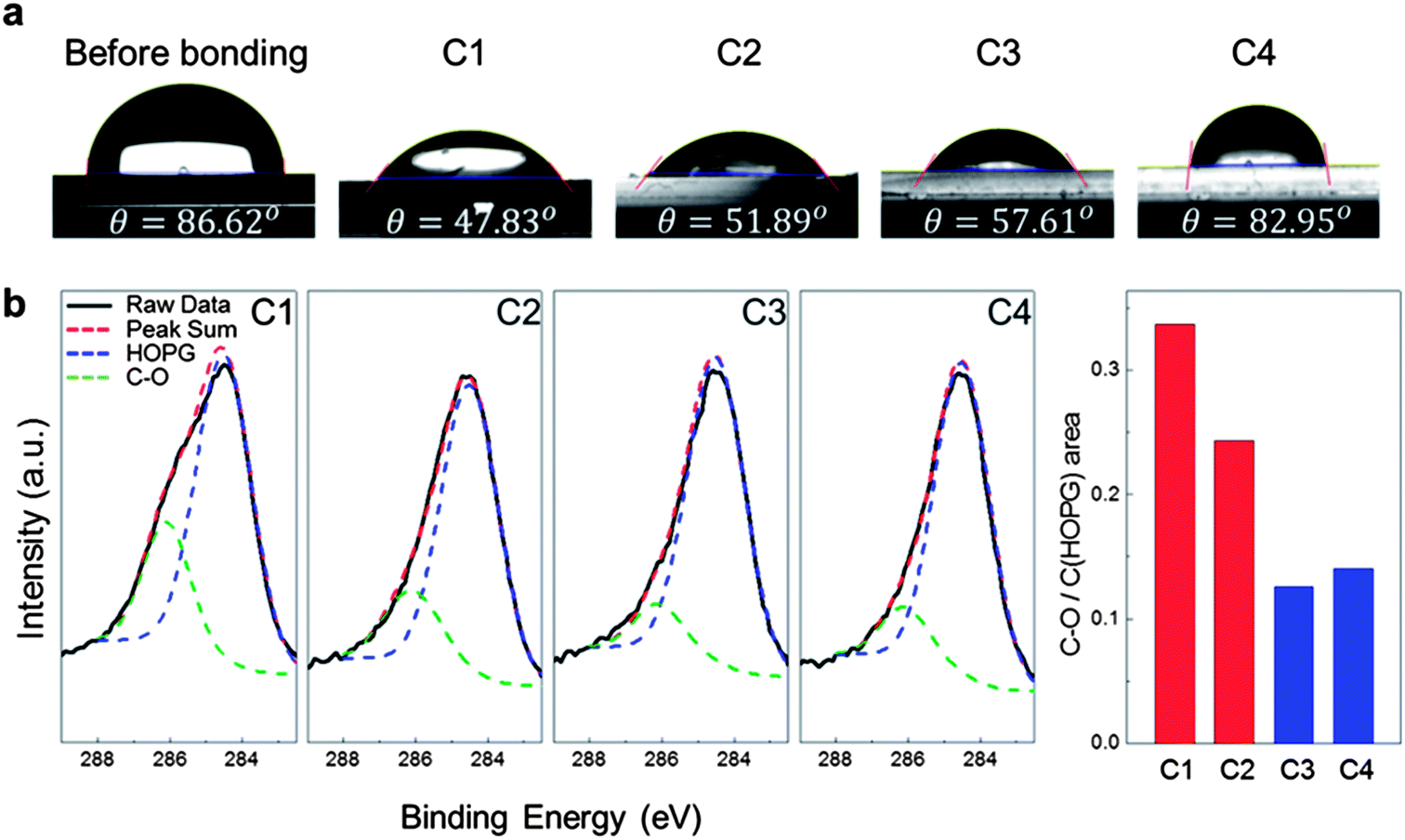 | ||
| Fig. 5 Water contact angle measurement and XPS analysis of the fractured surfaces: (a) water contact angles were measured before bonding and after the DCB test under each condition. (b) Fitted curves of the XPS data in a binding energy range of 289 to 282 eV under each condition. The HOPG peak and the C–O peak are considered. Area ratios of each peak are calculated and they show that dense C–O bonds are formed on the glass substrate under C1 and C2 conditions. | ||
Conclusions
This paper reports an adhesion energy of 1.4 J m−2 for an adhesive of monolayer graphene, which is 310% stronger than van der Waals bonding. This ultra-thin graphene adhesive decreases the adhesive thickness from several tens of microns to 0.34 nm for epoxy or glue. This newly suggested bonding method may pioneer a new research use for graphene as an adhesive that can accelerate the timetable for application of electronic packaging devices, flexible displays, and NEMS devices.Experimental
Growth method of graphene
Monolayer graphene was grown on 25 μm thick copper (Cu) foil (99.8%, Alfa Aesar, item no. 13382) using a thermal CVD system. The Cu foil was annealed in a quartz tube at 1000 °C with a H2 flow of 6 sccm for 30 min at low pressure. Graphene was then synthesized on the foil at 1000 °C by introducing CH4:H2 (105:6 sccm) for 20 min at 0.45 Torr. After the growth process, the furnace was cooled to room temperature while only the H2 flow was maintained.Graphene wet transfer process
After the synthesis, one side of the copper foil specimen was spin-coated with polymethyl methacrylate (PMMA) to mechanically support the graphene layer during the transfer procedure to a substrate. The graphene layer on the other side was removed by oxygen plasma treatment. The specimen was floated on the surface of 0.1 M ammonium persulfate to separate the graphene/PMMA layer from the specimen by etching the Cu foil. The floating graphene/PMMA layer was subsequently transferred onto a silicon oxide substrate. The PMMA layer was removed by immersing the substrate in chloroform.Acknowledgements
This work was supported by the Global Frontier Research Center for Advanced Soft Electronics and NanoMaterial Fundamental Research from MEST in Korea and the Basic Science Research Program through the National Research Foundation of Korea (NRF) funded by the Ministry of Education, Science and Technology (2012R1A1A1006072).Notes and references
- S. Bae, H. Kim, Y. Lee, X. Xu, J.-S. Park, Y. Zheng, J. Balakrishnan, T. Lei, H. R. Kim, Y. I. Song, Y.-J. Kim, K. S. Kim, B. Özyilmaz, J.-H. Ahn, B. H. Hong and S. Iijima, Nat. Nanotechnol., 2010, 5, 574–578 CrossRef CAS PubMed.
- X. Li, W. Cai, J. An, S. Kim, J. Nah, D. Yang, R. Piner, A. Velamakanni, I. Jung, E. Tutuc, S. K. Banerjee, L. Colombo and R. S. Ruoff, Science, 2009, 324, 1312–1314 CrossRef CAS PubMed.
- S. P. Koenig, N. G. Boddeti, M. L. Dunn and J. S. Bunch, Nat. Nanotechnol., 2011, 6, 543–546 CrossRef CAS PubMed.
- J. S. Bunch, S. S. Verbridge, J. S. Alden, A. N. van der Zande, J. M. Parpia, H. G. Craighead and P. L. McEuen, Nano Lett., 2008, 8, 2458–2462 CrossRef CAS PubMed.
- C. Lee, X. Wei, J. W. Kysar and J. Hone, Science, 2008, 321, 385–388 CrossRef CAS PubMed.
- Z. Lu and M. Dunn, Appl. Phys., 2010, 107, 044301 Search PubMed.
- S. Scharfenberg, N. Mansukhani, C. Chialvo, R. L. Weaver and N. Mason, Appl. Phys., 2012, 100, 021910 Search PubMed.
- T. Yoon, W. C. Shin, T. Y. Kim, J. H. Mun, T.-S. Kim and B. J. Cho, Nano Lett., 2012, 12, 1448–1452 CrossRef CAS PubMed.
- M. J. Lee, J. S. Choi, J.-S. Kim, I.-S. Byun, D. H. Lee, S. Ryu, C. Lee and B. H. Park, Nano Res., 2012, 5, 710–717 CrossRef CAS PubMed.
- H. Yang, J. Heo, S. Park, H. J. Song, D. H. Seo, K.-E. Byun, P. Kim, I. Yoo, H.-J. Chung and K. Kim, Science, 2012, 336, 1140–1143 CrossRef CAS PubMed.
- S. M. Song and B. J. Cho, Nanotechnology, 2010, 21, 335706 CrossRef PubMed.
- O. Leenaets, B. Partoens and F. M. Peeters, Phys. Rev. B: Condens. Matter Mater. Phys., 2008, 77, 125416 CrossRef.
- L.-Y. Lin, D.-E. Kim, W.-K. Kim and S.-C. Jun, Surf. Coat. Technol., 2011, 205, 4864–4869 CrossRef CAS PubMed.
- Y. Shao, S. Zhang, C. Wang, Z. Nie, J. Liu, Y. Wang and Y. Lin, J. Power Sources, 2010, 195, 4600–4605 CrossRef CAS PubMed.
- H. Wu, D. Wexler and H. Liu, J. Solid State Electrochem., 2011, 15, 1057–1062 CrossRef CAS PubMed.
- V. Huc, N. Bendiab, N. Rosman, T. Ebbesen, C. Delacour and V. Bouchiat, Nanotechnology, 2008, 19, 455601 CrossRef PubMed.
- Q.-Y. Tong and U. Gösele, Semiconductor Wafer Bonding, Wiley, 1999 Search PubMed.
- G. Kräuter, A. Schumacher and U. Gösele, Sens. Actuators, A, 1998, 70, 271–275 CrossRef.
- J. Kim and C. C. Lee, Mater. Sci. Eng., A, 2006, 417, 143–248 CrossRef PubMed.
- G. Wallis, Electrocomponent Sci. Technol., 1975, 2, 45–53 CAS.
- E. Collart, A. Shukla, F. Gélébart, M. Morand, C. Malgrange, N. Bardou, A. Madouri and J.-L. Pelouard, J. Synchrotron Radiat., 2005, 12, 473–478 CrossRef CAS PubMed.
- A. Balan, R. Kumar, M. Boukhicha, O. Beyssac, J.-C. Bouillard, D. Taverna, W. Sacks, M. Marangolo, E. Lacaze, R. Gohler, W. Escoffier, J.-M. Poumirol and A. Shukla, J. Phys. D: Appl. Phys., 2010, 43, 374013 CrossRef.
- D. Briand, P. Webber and N. F. de Rooij, Sens. Actuators, A, 2004, 114, 543–549 CrossRef CAS PubMed.
- K. B. Albaugh, J. Electrochem. Soc., 1991, 138, 3089–3094 CrossRef CAS PubMed.
- T. Moldt, A. Eckmann, P. Klar, S. V. Morozov, A. A. Zhukov, K. S. Novoselov and C. Casiraghi, ACS Nano, 2011, 5, 7700–7706 CrossRef CAS PubMed.
- A. Shukla, R. Kumar, J. Mazher and A. Balan, Solid State Commun., 2009, 149, 718–721 CrossRef CAS PubMed.
- A. N. Sidorov, M. M. Yazdanpanah, R. Jalilian, P. J. Ouseph, R. W. Cohn and G. U. Sumanasekera, Nanotechnology, 2007, 18, 135301 CrossRef PubMed.
- A. B. Kuzmenko, E. van Heumen, F. Carbone and D. van der Marel, Phys. Rev. Lett., 2008, 100, 117401 CrossRef CAS.
- R. Knechtel, M. Knaup and J. Bagdahn, Microsyst. Technol., 2006, 12, 462–467 CrossRef CAS PubMed.
- S.-W. Choi, W.-B. Choi, Y.-H. Lee, B.-K. Ju, M.-Y. Sung and B.-H. Kim, J. Electrochem. Soc., 2002, 149, G8–G11 CrossRef CAS PubMed.
- A. K. Geim and K. S. Novoselov, Nat. Mater., 2007, 6, 183–191 CrossRef CAS PubMed.
- T. L. Cottrell, The Strengths of Chemical Bonds, Butterworths, London, 2nd edn, 1958 Search PubMed.
- P.-G. Ren, D.-X. Yan, X. Ji, T. Chen and Z.-M. Li, Nanotechnology, 2011, 22, 055705 CrossRef PubMed.
- A. K. Geim, Science, 2009, 324, 1530–1534 CrossRef CAS PubMed.
- L. Gao, W. Ren, H. Xu, L. Jin, Z. Wang, T. Ma, L.-P. Ma, Z. Zhang, Q. Fu, L.-M. Peng, X. Bao and H.-M. Cheng, Nat. Commun., 2012, 3, 699 CrossRef PubMed.
- L. Wang, J. Zhao, Y.-Y. Sun and S. B. Zhang, J. Chem. Phys., 2011, 135, 184503 CrossRef PubMed.
- A. Eckmann, A. Felten, A. Mishchenko, L. Britnell, R. Krupke, K. S. Novoselov and C. Casiraghi, Nano Lett., 2012, 12, 3925–3930 CrossRef CAS PubMed.
- Y. Y. Wang, Z. H. Ni, T. Yu, Z. X. Shen, H. M. Wang, Y. H. Wu, W. Chen and A. T. S. Wee, J. Phys. Chem. C, 2008, 112, 10637 CAS.
- E. S. Hung and S. D. Senturia, J. Microelectromech. Syst., 1999, 8, 497–505 CrossRef.
- R. Frye, J. Griffith and Y. Wong, Journal of the Electromechanical Society, 1986, 133, 1673–1677 CrossRef CAS PubMed.
- P. Nitzsche, K. Lange, B. Schmidt, S. Grigull and U. Kreissig, J. Electrochem. Soc., 1998, 145, 1755–1762 CrossRef CAS PubMed.
- K. V. Emtsev, F. Speck, Th. Seyller and L. Ley, Phys. Rev. B: Condens. Matter Mater. Phys., 2008, 77, 155303 CrossRef.
Footnotes |
| † Electronic supplementary information (ESI) available. See DOI: 10.1039/c3nr03822j |
| ‡ These authors contributed equally to this work. |
| This journal is © The Royal Society of Chemistry 2014 |