DOI:
10.1039/C3NJ00924F
(Paper)
New J. Chem., 2014,
38, 255-259
Morphological and optoelectronic studies on poly-crystalline leaf-like cobalt selenide thin film synthesized using a chemical bath deposition technique
Received
(in Montpellier, France)
12th August 2013
, Accepted 4th October 2013
First published on 7th October 2013
Abstract
The inorganic material cobalt selenide (CoSe), in crystalline form, possesses an optimal band gap matchable to the maximum of the solar spectrum, a high optical absorption coefficient and good conductivity. These characteristics make it quite suitable for use as a photo-electrode in solar conversion devices. However, it is difficult to obtain crystalline, uniform and stoichiometric deposits by conventional methods due to the large difference in their melting points. In view of this, we present a facile, low temperature chemical bath deposition route for the synthesis of highly ordered cobalt selenide thin films. Cobalt nitrate, sodium selenosulphate and ammonia were employed for the synthesis. The films were characterized using X-ray diffraction, optical absorbance, photoluminescence, electrical conductivity, scanning electron microscopy and EDS techniques. The analysis revealed a poly-crystalline structure in a stoichiometric, cubic form with a leaf-like morphology. The size and shape of the ‘leaf’ structure was observed to be uniform. A band gap of 1.7 eV was observed. The room temperature photoluminescence spectra displayed a strong, symmetrical peak at 1.7 eV confirming the directness of the band gap, while the conductivity measurements confirmed the semiconducting nature of the film with a single type of conduction mechanism. As per our literature survey on the chemical synthesis, this is the first attempt for the synthesis of poly-crystalline CoSe in thin film form.
Introduction
There has been growing interest in developing the thin films of late transition metal selenides for optoelectronic applications because of their characteristics such as band gaps matchable to the maximum of the solar spectrum, high optical absorption, good electrical conductivity, etc.1–3 Besides, the properties of selenium based compounds cover the range of ionic crystal–semiconductor–metal–superconductor including ferro- and ferri-magnetism. These properties make the alloy useful in electrical, optical and magnetic devices such as power switches, sensors, magnetic devices, ion selective membranes, etc.4–6 Cobalt selenide, a member of the transition metal selenides, shows promising properties such as a high optical absorption coefficient (105 cm−1), a matchable band gap (∼1.5 eV) and a good electrical conductivity. Cobalt selenide has been used as an efficient catalyst for oxygen reduction reactions8,9 and recently, an electrodeposited CoSe film has been used in solar energy conversion.10 A solar to electrical conversion device requires a photo-electrode material of high quality with a specific morphology. The growing of the desired size and shaped absorber is however, a challenging task to the scientific community. A nano or polycrystalline thin film can exhibit a high surface to volume ratio, which, with the correct choice of methodology, could lead to materials with desired morphologies so that a large quantum of solar energy can be absorbed for solar energy conversion. These materials can also be used as adsorbents in waste water treatment.6,7
So far, several ‘bottom up’ methods such as electro-deposition,11 hydrothermal,12 sputtering,13 alloying and high temperature4 processing have been employed for the synthesis of polycrystalline CoSe thin films. These methods have their own merits and demerits. Techniques such as electro-deposition, sputtering, etc. are based on gathering atoms in a random manner (so called ‘atom bottom up’), which results in the formation of a non-stoichiometric, sub-quality material containing impurities and vacancies so that further processing is needed to obtain device quality.14 Furthermore, techniques such as vapor deposition, molecular beam epitaxy, alloying, etc. work at specific unified temperatures and are therefore unable to produce stoichiometric compounds due to a large difference in the melting points of their constituent atoms; viz. cobalt (1495 °C) and selenium (217 °C).4 A chemical bath deposition (CBD) method, on the other hand, seems to be a recipe oriented, rapid, cost effective technique to evolve films. The stoichiometry of a film is maintained as the process involves the building up of oppositely charged ions rather than atoms (so called ‘ion bottom up’). Also, CBD is known for its low operating temperature, simplicity in processing, large scale capability and controllability.15,16
The present paper reports, for the first time, the synthesis of leaf-like poly crystalline CoSe thin films using the CBD method. So far, we could locate only a lone reference in the literature which reports the formation of amorphous CoSe using CBD.17 The morphology, crystalline properties and compositions of the thin films were characterized by scanning electron microscopy (SEM), X-ray diffraction analysis (XRD) and energy-dispersive X-ray analysis (EDS). Optical, photoluminescence and electrical conductivity studies were performed to characterize the material.
Experimental methods
Preparation of reagents
All chemicals used were of analytical grade (A. R). They include cobalt nitrate [Co(NO3)2·4H2O], liquor ammonia (25% liq. NH3), anhydrous sodium sulfite (Na2SO3), triethanolamine (TEA) and selenium powder (Thomas Baker). All the solutions were prepared in double distilled water. A sodium selenosulphate (Na2SeSO3) solution was prepared by refluxing 5 g of selenium powder and 15 g of sodium sulfite in 200 mL of double distilled water for 9 h at 363 K.15 The resulting solution was cooled, filtered to remove the undissolved selenium and stored in an airtight container. The deposition was carried out on commercially available, non-conducting micro-glass slides (Blue Star, India) having dimensions of 75 × 25 × 1.35 mm. The slides were cleaned by washing with chromic acid for one hour followed by rinsing in acetone and finally with double distilled water.
Deposition of a cobalt selenide thin film
In a typical experiment, to 10 mL (0.25 M) of cobalt nitrate solution (in 250 mL beaker), 20 mL of triethanolamine (TEA) followed by 40 mL of liquor ammonia were added drop-wise with constant, vigorous stirring. To this, 10 mL (0.25 M) of sodium selenosulphate was added at room temperature and the final volume was made up to 180 mL by adding double distilled water. The pH of the reactive mixture was maintained at 8.5 ± 0.5. The beaker was then kept in an oil bath. The clean glass slides, vertically positioned on a specially designed substrate holder, were rotated in the reaction mixture with a precisely controlled speed of 35 ± 2 rpm. The temperature of the bath was then allowed to increase slowly up to 343 K in a period of 180 minutes. After the stipulated period, the slides were removed, washed several times with double distilled water, dried naturally and preserved in the dark in desiccators over anhydrous CaCl2.
Characterization
The XRD study of the CoSe thin film was carried out in the diffraction angle (2θ) range of 10–80° with CuKα1 (λ = 1.54056 Å) radiation using a Philips PW-1710 diffractometer. The thickness of the film was estimated by using a weight-difference method. The electrical conductivity of the CoSe thin film was measured using a ‘dc’ four probe (equal spacing) method. Thermoelectric measurements were carried out by maintaining a temperature gradient along the length of a film and measuring the potential difference developed across the points separated by one centimeter. The optical absorption measurements were made in the wavelength range 400–1200 nm by using a UV 3600 Shimadzu UV-VIS-NIR double beam spectrophotometer at room temperature. An identical, uncoated glass substrate in the reference beam made a substrate absorption correction. The photoluminescence (PL) spectra were measured on a Jasco spectrofluorometer (FP-8300, Japan) at an excitation wavelength of 580 nm. Scanning electron microscopy (SEM) was used for microscopic observations. The EDS attached to the scanning electron microscope was used for compositional analysis.
Results and discussion
Growth mechanism
The rate of deposition of the CoSe thin film depends on the super saturation, pH and temperature of the bath and the composition of the reactive constituents. We performed a series of experiments to optimize various parameters to get a good quality and reproducible film. At 298 K, the reaction mixture is a clear solution (i.e. a homogeneous system). A slow increase in temperature allows the decomposition of sodium selenosulphate and the metal complex in the alkaline medium generating ions which combine on the substrate giving the thin film. The deposition process is based on the slow release of Co2+ ions and Se2− ions followed by an ion-by-ion combination procedure. The deposition takes place when the ionic product of Co2+ and Se2− exceeds the solubility product. The thickness of the CoSe thin film was measured using a weight difference density consideration technique and was found to be 1.1 μm.
The morphological aspect of the film discussed in this section of the paper is typically a columnar–leaf-like structure. This can be explained within the context of a typical geometry of the deposition system used. The circular motion of the substrate at limited speed (∼35 rpm) in the reaction solution bath sets the ions in motion. The flat substrate (while moving) pushes the ions in an outward direction. This gives a unique, centrifugal type mobility to the ions. As the speed is low, the nucleation centers on the film grow to give the columnar film. This type of structure is commonly observed when the depositing ions/atoms have limited mobility.18
The overall growth of the film can be understood from the following reactions:
| | | [Co(NH3)4]2+ ↔ Co2+ + 4NH3 | (1) |
| | | Na2SeSO3 + 2OH− → Se2− + Na2SO4 + H2O | (2) |
Various factors were found to be very critical in getting the deposits. Any changes in pH whilst keeping the temperature constant, and vice versa, results in no deposition except at pH: 8.5 and working temperature: 338 K. The duration of the film deposition, optimized to get an overgrowth free film is 180 min, while the speed of rotation was finalized at ∼35 rpm.
X-Ray diffraction analysis
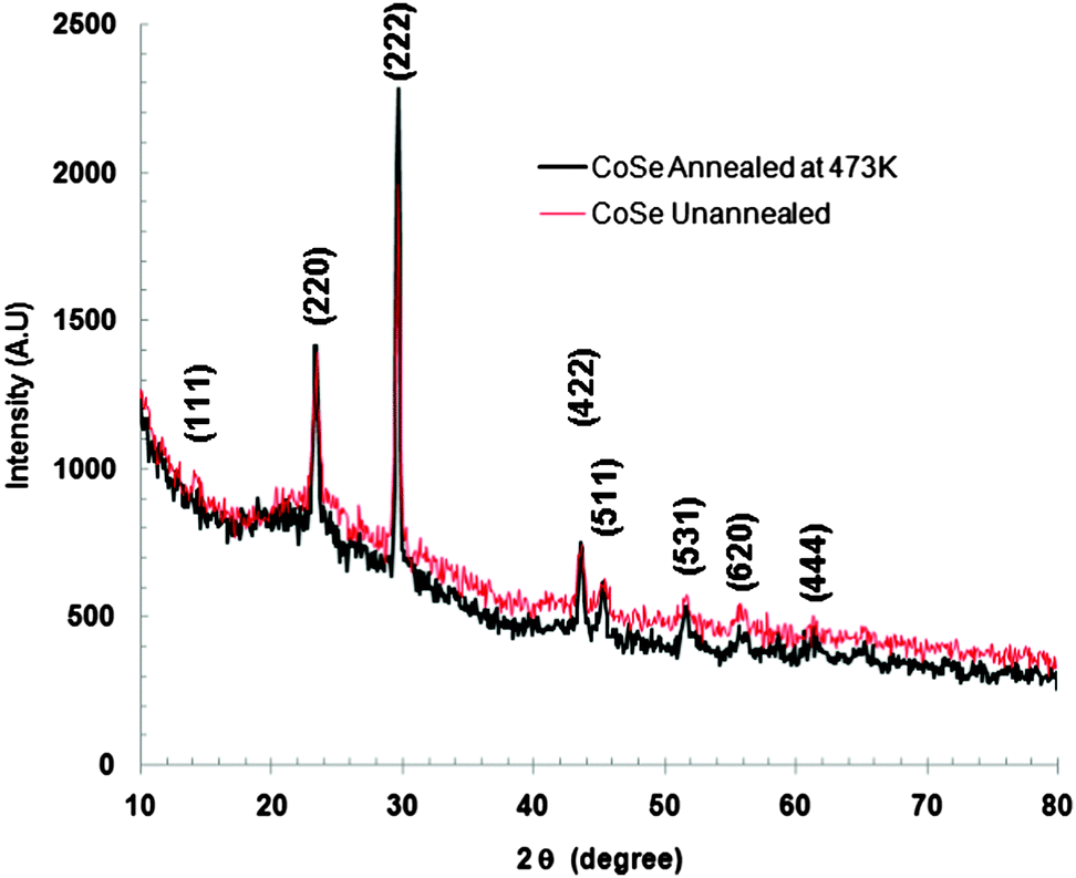
X-Ray diffraction was employed for studying the structural details of the as-deposited CoSe thin film. The XRD patterns of the as-deposited CoSe film and that annealed at 473 K in air (for 2 h) are shown in Fig. 1.
 |
| | Fig. 1 X-ray diffraction patterns of the as-deposited (unannealed) and annealed CoSe thin films. | |
The well defined and narrow peaks in the XRD pattern of the as-deposited CoSe film indicate that the film is polycrystalline in nature. The X-ray diffraction pattern shows diffraction peaks at the following 2θ angles; 14.77, 23.95, 29.71, 43.48, 45.31, 51.76, 55.71 and 61.63 degrees corresponding to the crystallographic orientations (111), (220), (222), (422), (511), (531), (620) and (444), respectively, according to the JCPDS card number 09-0233 for CoSe indicating that the film is cubic Co9Se8. The lattice parameter of the film was found to be 10.39 Å which is in good agreement with the JCPDS card value. It is important to note here that all methods except CBD usually produce a range of non-stoichiometric compounds based on the formula Co1−xSe (0 < x < 0.25).11 The non-stoichiometry is usually associated with cobalt vacancies. The X ray diffraction pattern of the CoSe film annealed at 473 K in air (for 2 h) exhibits a similar pattern to that of the as-deposited film except there is a little increase in intensity of the diffraction peaks indicating that the as-deposited CoSe film is being deposited in a well crystallized form.
Morphological and compositional analysis
The scanning electron micrographs of the as-deposited cobalt selenide thin film are shown in Fig. 2 under different magnifications.
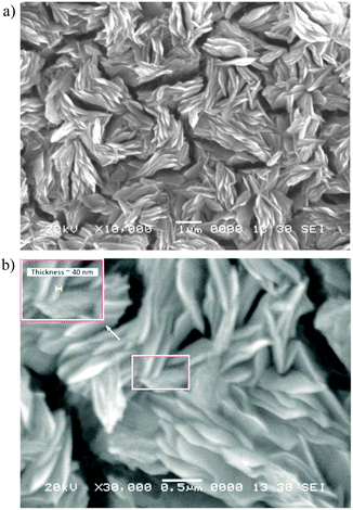 |
| | Fig. 2 Scanning electron micrographs of leaf-like CoSe: (a) under 10![[thin space (1/6-em)]](https://www.rsc.org/images/entities/char_2009.gif) 000× magnification and (b) under 30000× magnification. 000× magnification and (b) under 30000× magnification. | |
The surface morphology exhibited by the as-deposited CoSe is leaf-like with an almost uniform individual leaf thickness. The size and shape of the individual leaves are found to be quite uniform. The inset of Fig. 2b shows the magnification of the portion highlighted by a white rectangle. The thickness of a leaf was estimated to be around 40 nm with a length of about 1–2 μm. This chemically deposited thin film has, for the first time, shown a unique morphology without further processing of the film. This type of morphology possesses a large surface to area ratio and is, therefore, quite suitable for receiving large solar radiation in solar energy conversion devices.
The elemental qualitative analysis of the cobalt selenide thin film was carried out by using energy dispersive X-ray analysis (EDS). The EDS spectrum showed peaks corresponding to Co and Se transitions with a Co:Se atomic mass percentage ratio of 52.58:47.42, representing a stoichiometry close to Co9Se8.
Optical properties
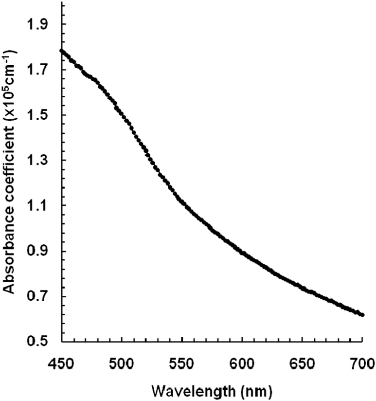
The optical absorption spectrum of the as-deposited cobalt selenide thin film was recorded on a double beam spectrophotometer at the wavelength range of 400 to 1200 nm at room temperature. The reflectance and refraction losses were negated. Fig. 3 shows the optical absorption spectrum of the as-deposited cobalt selenide thin film. It shows a steep increase in the absorption with a decrease in the wavelength beyond 650 nm. The optical absorption coefficient was calculated by using the Lambert law.19| | | ln[I0/I] = 2.303A = αd | (4) |
Where I0 and I are the intensities of the incident and transmitted light, respectively; α is the absorption coefficient, A is the optical absorption and d is the thickness of film. The literature reported value of the optical absorption coefficient for CoSe was of the order of 104 cm−1. The value for the thin film of CoSe is however, not available in the literature. For the CoSe thin film, we observed an optical absorption coefficient of the order of 105 cm−1.
 |
| | Fig. 3 Optical absorption spectrum of the CoSe thin film. | |
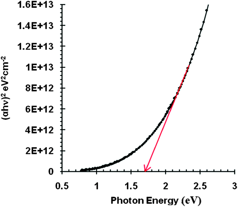
The variation of the absorption coefficient function i.e. α = f(hν) with wavelength is shown in Fig. 4. The band gap of a material obeys the relation near the absorption edge, according to Bardeen et al.20
Where
B is a constant,
hν is the wavelength of the light used,
Eg is the band gap of the material and
x is a factor that depends on the kind of transitions involved. The value of
x corresponding to 1/2 indicates the presence of a direct allowed transition. Rearranging
eqn (5) to an equation for a linear line,
viz. y =
mx +
c, gives
y = (
αhν)
2,
x =
hν, the linear portion of which can be extrapolated to the
x axis to give a value for the band gap (
Eg). Accordingly,
Fig. 4 shows a plot of absorption coefficient (
αhν)
2vs. photon energy. The extrapolation of a linear portion of the graph gives a direct band gap (
Eg) of 1.70 eV at room temperature. The value of the band gap is higher than the reported value (1.53 eV).
13,21 The higher band gap observed for CoSe could be ascribed to the size quantization effect caused by the nano-leaf-like structure.
22
 |
| | Fig. 4 Plot of (αhν)2vs. hν for the CoSe thin film. | |
Electrical properties
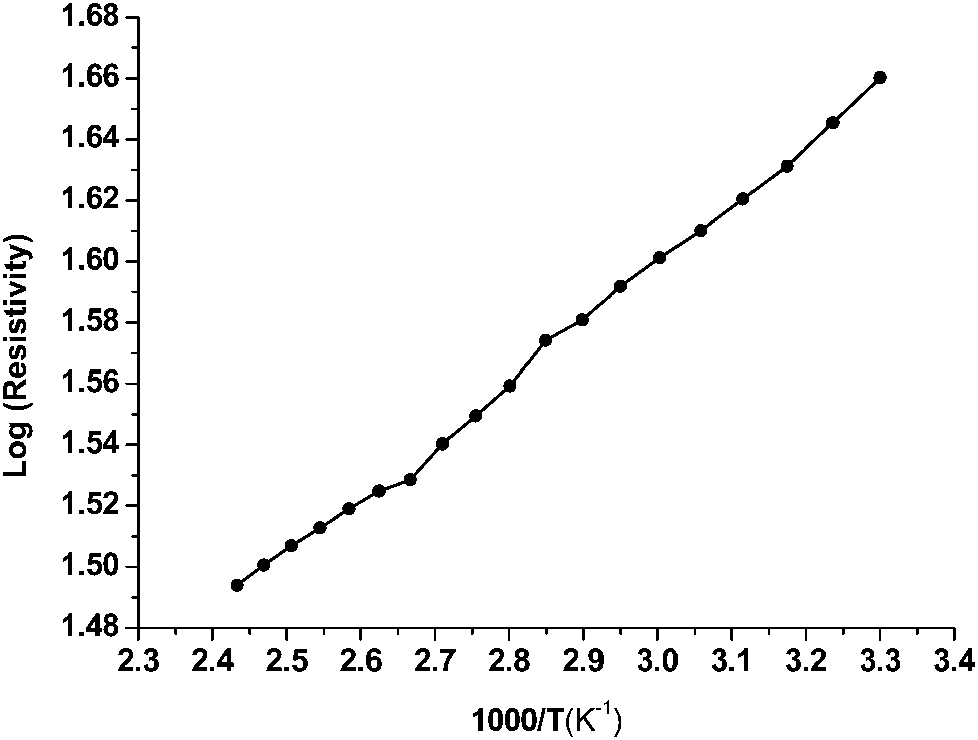
The electrical resistivity of the as-deposited CoSe thin film was measured in the 300–500 K temperature range. The room temperature sheet resistance for the 1.1 μm thick film was observed to be 1.988 × 10⁴ Ω. It is observed that the resistivity decreases with increasing temperature, indicating the semiconducting nature of the material. It is well known that the electronic properties of thin film materials are strongly dependent on the nature of impurities.23,24 The type of conductivity of a film material can be determined from the temperature dependence of the electrical resistivity of the material which follows the Arrhenius relation:where Ea is the activation energy, k is the Boltzmann constant; T is the absolute temperature, and ρ and ρo are the resistivity and specific resistivity, respectively. The nature of the logρ vs. inverse absolute temperature plot is linear, indicating that there is the presence of only one type of conduction mechanism (Fig. 5). The activation energy of the CoSe film calculated from the above plot was found to be 0.388 eV. The thermo-emf generated when a temperature gradient was applied across the length of CoSe film showed a negative polarity toward the cold end indicating n-type conduction carriers.
 |
| | Fig. 5 Plot of logρ vs. inverse absolute temperature. | |
Photoluminescence (PL) studies
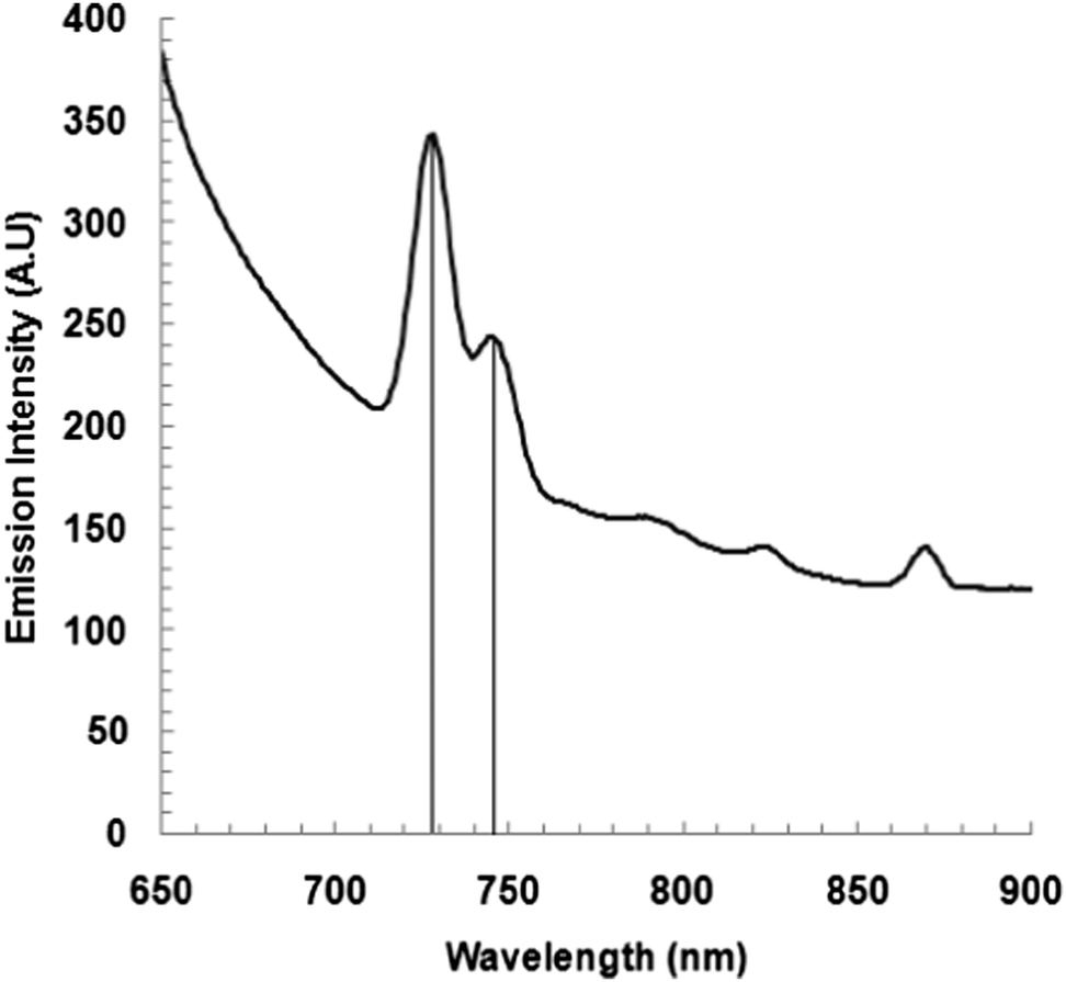
Photoluminescence (PL) spectroscopy at room temperature has received increasing interest as it is a non-destructive technique used to characterize the quality of a semiconductor material. The PL mapping of the band edge emission and deeper defect related emission has proven to be a useful technique to characterize the homogeneity, stoichiometry and presence of defects along with the nature of defect, doping level, etc.25 The photoluminescence spectrum of the as-deposited CoSe at an excitation wavelength of 580 nm was obtained at RT and is shown in Fig. 6. The spectrum showed a strong, visible, symmetrical emission peak at a wavelength of 730 nm (i.e. 1.7 eV) and a small peak shoulder at 745 nm (1.66 eV). The strong emission at 1.7 eV appears to be due to an excitonic band to band (e–h) recombination, the value exactly matching that computed from absorption measurements, while a peak at 1.66 eV is attributed to a transition from shallow trap centers to the conduction band.25
 |
| | Fig. 6 PL spectrum of CoSe at an excitation wavelength of 580 nm. | |
Conclusion
A conventional chemical bath deposition method has been used to fabricate a polycrystalline CoSe thin film for the first time. The chemically deposited thin film showed a unique leaf-like morphology. The CoSe film exhibits a good stoichiometry, high absorption coefficient, direct band gap of 1.7 eV and good conductivity with a single type of conduction. Furthermore, the leafy morphology possesses a large surface to area ratio, therefore CoSe is quite suitable for use as a photo electrode in solar energy to electrical conversion devices.
Acknowledgements
The authors MLG and VMB are grateful to the Director of Higher Education, Pune, India for giving permission to carry out the research work.
References
- P. P. Hankare, B. V. Jadhav, K. M. Garadkar, P. A. Chate, I. S. Mulla and S. D. Delekar, J. Alloys Compd., 2010, 490, 228–231 CrossRef CAS PubMed.
- Y. Takemura, H. Suto, N. Honda, K. Kakuno and K. Saito, J. Appl. Phys., 1997, 81, 5177–5179 CrossRef CAS.
- Z. Zainal, N. Saravanan and H. L. Mien, J. Mater. Sci.: Mater. Electron., 2005, 16, 111–117 CrossRef CAS PubMed.
- J. C. de Lima, T. A. Grandi, K. D. Machado and P. S. Pizani, Phys. B, 2002, 324, 409–418 CrossRef.
- S. M. Pawar, A. V. Moholkar, U. B. Suryavanshi, K. Y. Rajapure and C. H. Bhosale, Sol. Energy Mater. Sol. Cells, 2007, 91(7), 560–565 CrossRef CAS PubMed.
- J. F. Zhao, J. M. Song, C. C. Liu, B. H. Liu, H. L. Niu, C. J. Mao, S. Y. Zhang, Y. H. Shen and Z. P. Zhang, CrystEngComm, 2011, 13, 5681–5684 RSC.
- G. Chen, J. Seo, C. Yang and P. N. Prasad, Chem. Soc. Rev., 2013, 42, 8304 RSC.
- Y. Feng and N. A-Vente, Electrochim. Acta, 2012, 72, 129–133 CrossRef CAS PubMed.
- P. Nekooi, M. Akari and M. K. Amini, Int. J. Hydrogen Energy, 2010, 35, 1392–1398 CrossRef PubMed.
- Y. Lai, F. Liu, J. Yang, B. Wang, J. Lai and Y. Liu, Appl. Phys. Express, 2011, 4, 71201 CrossRef.
- F. Liu, B. Wang, Y. Lai, J. Li, Z. Zang and Y. Liu, J. Electrochem. Soc., 2010, 157, D523–D527 CrossRef CAS PubMed.
- W. Zhang, Z. Yang, J. Liu, Z. Hui, W. Yu, Y. Qian, G. Zhou and L. Yang, Mater. Res. Bull., 2000, 35, 2403–2408 CrossRef CAS.
- L. Zhu, D. Susac, A. Lam, M. Teo, P. C. Wong, D. Bizzotto, S. A. Campbell, R. R. Parsons and K. A. R. Mitchell, J. Solid State Chem., 2006, 179, 3942–3948 CrossRef CAS PubMed.
- S. N. Yakunin and N. N. Dremova, JETP Lett., 2008, 87(9), 494–497 CrossRef CAS.
- U. R. Dappadwad, M. K. Lande, S. G. Chonde, B. R. Arbad, P. P. Hankare and V. M. Bhuse, Mater. Chem. Phys., 2008, 112, 941–944 CrossRef CAS PubMed.
- V. M. Bhuse and P. P. Hankare, Ionics, 2004, B10(3&4), 304–310 Search PubMed.
- P. Pramanik, S. Bhattacharya and P. K. Basu, Thin Solid Films, 1987, 149, L81–L84 CrossRef CAS.
-
M. Ohring, Material science of thin film deposition and structure, Academic Press, San Diego, 2002 Search PubMed.
- N. Kumar, V. Sharma, U. Parihar, R. Sachdeva, N. Padha and C. J. Panchal, J. Nano- Electron. Phys., 2011, 3, 117 Search PubMed.
-
J. Bardeen, F. J. Blatt and L. H. Hall, in Proceedings of the photoconductivity conference, ed. R. Brechenridge, B. Russel and T. Hahn, Wiley, New York, 1975, p. 90 Search PubMed.
- B. Wang, F. Y. J. Li, Y. Q. Lai, Z. A. Zang and Y. X. Liu, Int. J. Inorg. Mater., 2011, 26(4), 403–410 CrossRef CAS.
- A. L. Stroyuk, A. I. Kryukov, S. Ya. Kuchmii and Y. D. Pokhodenka, Theor. Exp. Chem., 2005, 41(2), 67 CrossRef CAS PubMed.
- P. P. Hankare, S. D. Delekar, P. A. Chate, M. R. Asabe, V. M. Bhuse, A. S. Khomane, K. M. Garardkar and B. D. Sarwade, J. Phys. Chem. Solids, 2006, 67, 2506–2511 CrossRef CAS PubMed.
- M. J. Deen and F. Pascal, J. Mater. Sci.: Mater. Electron., 2006, 17, 549–575 CrossRef CAS PubMed.
-
P. T. Landsberg, in Recombinations in Semiconductors, Cambridge University, Cambridge, 1991 Search PubMed.
|
| This journal is © The Royal Society of Chemistry and the Centre National de la Recherche Scientifique 2014 |
Click here to see how this site uses Cookies. View our privacy policy here.