Thin film synthesis and properties of copper nitride, a metastable semiconductor†
Christopher M.
Caskey
*ab,
Ryan M.
Richards
b,
David S.
Ginley
a and
Andriy
Zakutayev
a
aNational Renewable Energy Laboratory, Golden, Colorado, USA. E-mail: chris.caskey@nrel.gov
bDepartment of Chemistry and Geochemistry, Colorado School of Mines, Golden, Colorado, USA
First published on 16th April 2014
Abstract
Copper nitride (Cu3N) thin films were grown by reactive sputtering using a high-throughput combinatorial approach with orthogonal gradients of substrate temperature and target–substrate distance. This technique enables high-throughput modulation of the anion activity, and is broadly applicable to the combinatorial synthesis of other materials. Stable, phase pure Cu3N thin films were grown on glass substrates at temperatures between 150 and 200 °C, depending on the target–substrate distance. These 00L oriented thin films have 10−3 S cm−1 conductivity and 1.5 eV optical absorption onset, making Cu3N interesting for future studies in the context of solar energy conversion applications. The analysis of the synthetic results provides insights into the thermodynamic origins of the growth of metastable Cu3N, and sets a nitrogen chemical potential of +1 eV per atom as a lower limit of the anion activity that can be achieved in non-equilibrium thin film growth of metastable materials. The first step towards testing the transferability of this result to other materials was made by reactive sputtering of tin, antimony, and bismuth in nitrogen.
Conceptual insightsThis work evaluates the potential for energy conversion applications of copper nitride, a rather unexplored simple binary metastable nitride semiconductor. Studying copper nitride in the context of solar energy conversion applications provides a conceptual advance in the field of optoelectronic nitride semiconductors, a field that so far has been limited to group III nitrides. Further, shown herein is a high-throughput method for varying the activity of the anion during sputtering. The high-throughput variation of nitrogen activity demonstrated in this paper represents a readily applicable advance in the field of combinatorial materials science, which to date primarily focused on varying cation composition. Finally, this work provides a framework for evaluating the likelihood of synthesizing other non-equilibrium materials. The rationalization of the thermodynamic metastability of the copper nitride material in terms of its convex hull and atomic nitrogen chemical potential is a conceptual insight in the field of materials-by-design, in particular computational materials prediction, and was extended to the nitrides of tin, antimony, and bismuth. |
Introduction
Semiconducting materials play an important role in modern technology due to their broad use in integrated circuits, chemical sensors, photodetectors, and other technologies. Of particular importance are the optoelectronic energy conversion applications of semiconductors, such as solar cells, light-emitting diodes, and photoelectrochemical devices. Thus the quest for new semiconducting materials, particularly earth-abundant non-toxic systems, is a major research thrust in the field of materials science. Copper nitride (Cu3N) is a non-toxic metastable semiconducting material composed of earth-abundant elements that has been proposed for applications in metallization layers,1–3 tunnel junctions,4 and resistive random-access memory (RRAM).5 Stoichiometric, nitrogen-rich, and copper-rich Cu3N materials have been previously reported.6–9 The published electrical conductivities vary from ∼30 S cm−1 (ref. 10) to ∼10−3 S cm−1 (ref. 11) and the published optical absorption onsets are in the range of 1.4 to 1.8 eV.7,11 There is disagreement regarding the value of the electronic band gap in Cu3N, some of which may be the result of inconsistent terminology,12 but reported values range from 0.25 eV to 1.90 eV.7,13 This range nevertheless suggests that the binary Cu3N has a potential as a solar absorber, and one of the goals of this work is to evaluate this possibility. The related ternary copper nitride CuTaN2, which has the same linear N–Cu–N structural motifs as Cu3N, has been recently reported to be promising for solar energy conversion applications because of its calculated band gap of 1.3 eV, measured absorption onset at 1.5 eV, and large calculated absorption coefficient of 105 cm−1 just 0.1 eV above the onset.14 The N–Cu–N structural motifs in both Cu3N and CuTaN2 lead to anti-bonding character of the valence band maximum, which could result in tolerance of the electrical properties of these copper nitride materials to structural defects.15Most of the prior work on Cu3N has been in thin film form with the samples produced by reactive sputtering. In the reactive sputtering of Cu3N, nitrogen gas reacts with a copper metal target forming on its surface a copper nitride compound layer. Argon and nitrogen ions are created in plasma and accelerated by electric field towards the Cu target, sputtering off the compound layer. The sputtered Cu and N species, partially reacting in the gas phase, are collected on a glass substrate where the Cu3N compound re-forms. Since Cu3N is thermodynamically metastable with respect to decomposition into copper and nitrogen (+0.2 eV per atom),16 an important variable in the growth of Cu3N is the activity of nitrogen at the film surface. For a given partial pressure of nitrogen, nitrogen activity is expected to decrease with increasing target–substrate distance due to gas-phase recombination of sputtered N species, and to decrease with increasing substrate temperature due to N2 emission from the growing film. While the temperature10,11,13,17 and pressure6–8,11,17–19 variables of Cu3N growth have been investigated, the target–substrate distance effect on nitrogen activity has not been studied so far. In this work we study the effect of nitrogen activity on the synthesis, structure and properties of copper nitride by simultaneous control of the target–substrate distance and substrate temperature.
An efficient way to establish fundamental synthesis-structure–property relationships in materials is the thin film combinatorial approach.20 Our current implementation21 of this high-throughput experimental strategy relies on (a) establishing gradients in growth parameters across the substrate during synthesis, (b) measuring the properties of the resulting combinatorial libraries as a function of position, and (c) analysing the resulting large amounts of data in a semi-automated way. Current combinatorial literature contains many examples of cation composition gradients,22–26 and a few examples of substrate temperature gradients,27–31 however, anion activity so far has not been studied via a high-throughput method. The present work fills this gap by growing copper nitride thin films with orthogonal gradients of temperature (TS) and target–substrate distance (dTS), such that each point on the substrate experiences a unique combination of TS and dTS growth conditions. In this experiment, equivalent nitrogen activity is achievable by different combinations of TS and dTS, enabling direct mapping of the constant nitrogen activity contours as a function of these two variables.
Experimental
The copper nitride thin film sample libraries were deposited on glass substrates by radio-frequency (RF) reactive sputtering of copper in 10 mTorr of nitrogen supplied through an RF atom source, balanced by 10 mTorr of argon supplied through a mass flow controller. The substrate was mounted at 45° relative to the sputter gun, resulting in a dTS gradient of 13 to 15 cm. Only one side of the substrate was in thermal contact with a heater resulting in a TS gradient of 140–280 °C perpendicular to the dTS gradient. Each sample library was characterized at 88 points for phase purity using X-ray diffraction (XRD), for absorption properties using optical spectroscopy and for conductivity using sheet resistance measured by four-point probe combined with thickness measured by X-ray fluorescence (XRF). The morphology of selected sample areas was imaged with scanning electron microscopy (SEM). More details about the experimental methods can be found in the ESI† as well as our prior publications.23,25Results and discussion
As shown in Fig. 1, phase pure 00L oriented Cu3N thin films were produced at low substrate temperatures and short target–substrate distances. Higher synthesis temperatures and longer target–substrate distances resulted in randomly oriented Cu3N films, possibly seeded by nanoscale copper inclusions that are not detectable by XRD. The transition between the 00L oriented and the polycrystalline regions occurred between TS ≈ 200 °C at dTS = 13 cm and TS ≈ 140 °C at dTS = 15 cm. Crystalline copper inclusions and subsequently pure copper films were observed in the XRD at the highest temperatures and the longest target–substrate distances. Note that the co-existence of Cu and Cu3N indicates non-equilibrium synthesis according to the Gibbs phase rule. The production of both Cu1+ and Cu0 species in this experiment demonstrates that the anion activity was modulated by the simultaneous control of the substrate temperature and the target–substrate distance. This strategy may be also applicable to other material systems, as shown later in the paper for tin, antimony and bismuth.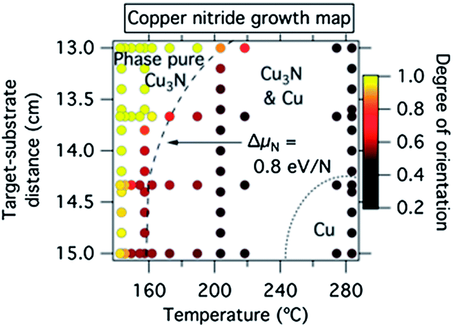 | ||
| Fig. 1 Copper nitride growth map as a function of substrate temperature and target–substrate distance. The dashed line separates growth conditions which produced phase pure Cu3N from those which produced Cu3N & Cu. Along this line ΔμN = +0.8 eV N−1. The dotted line separates growth conditions which produced Cu3N & Cu from those which produced Cu. The colour scale is the degree of crystallographic orientation and is the sum of the areas of the 001 and 002 peaks divided by the areas of the four measured Cu3N peaks, with the value of 0.3 corresponding to a randomly oriented film. | ||
There are two likely mechanisms that can explain the measured synthesis phase map of the metastable copper nitride (Fig. 1). The first mechanism, which is thermodynamic in nature, is that a sufficiently high concentration of reactive nitrogen species is present at the surface of the growing copper nitride film at low target–substrate distances (due to decreased opportunity for 2N/N2 gas phase neutralization) and low substrate temperatures (due to less likely reemission of N2 from the growing film). The second mechanism, kinetic in origin, is that the high arrival rates of copper and nitrogen atoms suppress the reemission of N2 by adding more material before molecular nitrogen can form. In order to test these two hypotheses, we compared the films grown with (i) the nitrogen atom source on (250 W) and off (0 W) and thus resulting in different concentrations of reactive nitrogen species, and (ii) with different power applied to Cu target (15 W, 20 W and 25 W) and thus resulting in different rates of arriving copper and nitrogen atoms. As shown in ESI Fig. S1,† the first experiment led to dramatic decrease in the size of the phase pure region while the second experiment did not significantly change the results when compared to Fig. 1. The results of these two experiments indicate that in the studied range of conditions the concentration of reactive nitrogen species rather than the rate of arrival of copper and nitrogen atoms controls the growth chemistry of copper nitride. Thus, sparingly, the driving force behind the synthesis of phase-pure metastable Cu3N can be viewed as thermodynamic rather than kinetic in its origin.
As show in Fig. 2, conductivities of the 00L oriented thin films deposited at <160 °C were consistently in the range of 5 × 10⁻⁴ S cm−1 to 2 × 10⁻³ S cm−1. The conductivity numbers and XRD patterns of these Cu3N samples did not change after 1+ years of sample storage at ambient conditions, suggesting that the films are shelf-stable. By increasing the substrate temperature to 170–220 °C, the conductivity rose by a factor of 10–1000, and for some of these samples copper inclusions were observed in the XRD (Fig. 2 right axis). Such inclusions or similar copper richness are possible reasons for large variations of copper nitride conductivity reported in the literature.7,32 Thin films deposited at 270–280 °C substrate temperature had 103 S cm−1 conductivity consistent with predominantly metallic copper clearly observed by XRD.
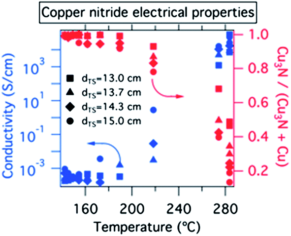 | ||
| Fig. 2 Electrical properties and phase purity of copper nitride thin films. The right axis is the area of Cu3N XRD peaks divided by the areas of Cu3N and Cu XRD peaks. Thus a value of unity corresponds to phase pure Cu3N. The spread of data for fixed TS results from the differences in dTS = 13.0, 13.7, 14.3 and 15.0 cm. | ||
As demonstrated in Fig. 3, for the phase pure 00L oriented Cu3N thin films grown at a substrate temperature of 160 °C and at short (13.0–13.5 cm) target–substrate distances, the optical absorption onset ranged from 1.4 to 1.6 eV and the onset was steepest (lower portion of Fig. 3a and b). In contrast, significant sub-gap absorption was observed in the polycrystalline samples grown at longer target–substrate distances with a decrease in the steepness of the onset (dashed line in Fig. 3a and b). Finally, small copper inclusions are observed in XRD at the longest target–substrate distances. At dTS = 15 cm, the sub-gap absorption increases significantly, presumably due to increased concentration of these metallic inclusions (upper trace in Fig. 3a and b). We note that Fig. 3a is very similar to the results obtained by Pierson when the flow rate and partial pressure of nitrogen was modulated:6 the present target–substrate distance gradient appears to mimic changes in partial pressure of nitrogen.
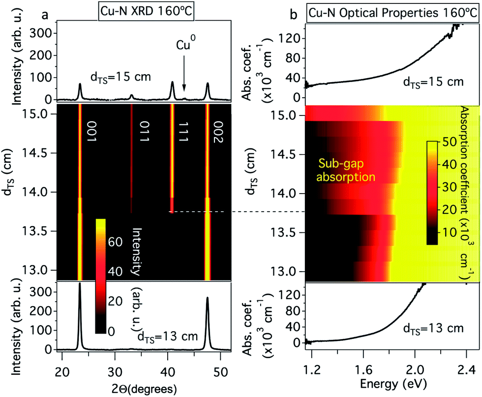 | ||
| Fig. 3 Structural and optical properties of Cu3N thin films: (a) XRD patterns and (b) optical absorption spectra at different target–substrate distances (dTS) and a constant substrate temperature of 160 °C. An alternative form of this figure is available in the ESI Fig. S2.† | ||
Synthesis of 00L oriented copper nitride thin films with low conductivity and no sub-gap absorption satisfies the minimal requirements for this material to be studied in the future as a solar absorber. However, optical absorption and electrical conductivity are not the only important parameters for this and other semiconductor applications. For example in photovoltaics, the minority carrier lifetime, which is determined by defect density (reflected by the measured sub-gap absorption), as well as the concentration and mobility of the majority charge carriers (on which the measured electrical conductivity depends), are crucial parameters for device performance and would need to be studied. We also note that the measured absorption onset (which defines the short-circuit current limit of a solar cell) does not necessarily correspond to the band gap (which sets the limit of the open-circuit voltage of a photovoltaic device), particularly for semiconductors that have an electronic structure with indirect or forbidden character of the band gap. Finally, the long-term operational performance of a metastable semiconductor like Cu3N would be necessary to consider. Future work will focus in more detail on the stability, transport, optical, and electronic structure properties of copper nitride with the goal to assess more rigorously its potential as a solar energy conversion material.
It is interesting to note that not only the phase purity and preferential orientation, but also the grain size of the copper nitride thin films depend on both substrate temperature and target–substrate distance. From the microscopy measurements shown in Fig. 4, films with small grains (30 to 50 nm) were observed in the 00L oriented regions at the lowest temperature and shortest target–substrate distance (Fig. 4a). Polycrystalline Cu3N films with grains of 50–100 nm (Fig. 4c) were grown at higher temperatures and longer target–substrate distances. A narrow band of 200 nm crystallites (Fig. 4c), visible to the eye as a dark stripe across the sample (Fig. 4 top left), was observed near the transition from textured to polycrystalline film. These 200 nm grains decreased in concentration with increasing distance from the transition region (Fig. 4 centre). The largest grains were 300 nm in size and were grown at a temperature of 230 °C, where copper inclusions were observed by XRD. Above this temperature the copper nitride decomposed, and the remaining copper was composed of complex, voided crystallites 100 to 200 nm in size. Cross-sections of the thin film regions with the 00L-textured (Fig. 4a) and polycrystalline (Fig. 4c) phase pure Cu3N revealed columnar structures while larger grains were observed in the transition region between these two limiting cases (Fig. 4b). While the mechanistic details of growth are not known, we propose that changes in anion activity leading to changes in energy, charge and composition of the grain surfaces are likely responsible for the observed variations in morphology. Specifically, we hypothesize that nitrogen-rich grain surfaces repel each other leading to small 00L oriented grains (Fig. 4a), copper-rich grain surfaces coalesce but seed small polycrystalline grains (Fig. 4c), and stoichiometric grain surfaces coalesce forming the largest grains in the narrow region between these cases (Fig. 4b). The elemental composition of the grains at the microstructure level is currently unknown. It is interesting that small changes in target–substrate distance and temperature have such dramatic affects on film morphology, and further tuning of these parameters could lead to intentional control of film roughness.
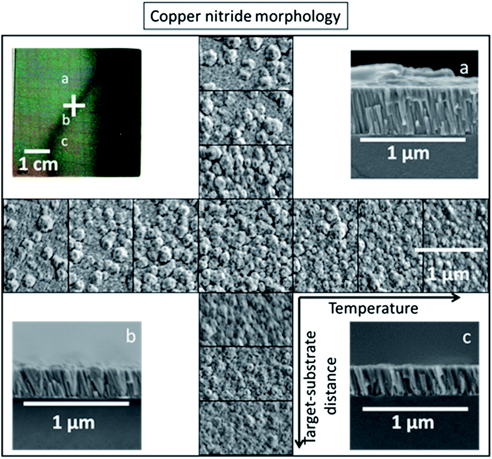 | ||
| Fig. 4 Morphological properties of the Cu3N thin films. Top left: photograph of a combinatorial thin film sample with the cross denoting the locations of SEM surface images (centre) and letters indicating locations of cross-sections. Centre: SEM surface images of copper nitride thin films taken 1 mm apart along the cross shown in the photograph. The cross-sectional images of the film are shown for the (a) 00L textured, (b) transition, and (c) polycrystalline regions of the film. | ||
The ability to synthesize phase pure Cu3N thin films with 00L orientation (Fig. 1), semiconducting properties (Fig. 2 and 3) and reasonable morphology (Fig. 4), despite the thermodynamically metastable character of this material may be attributed to the high energy of copper and nitrogen precursors used in the non-equilibrium sputtering process. In thermodynamic equilibrium, Cu3N is unstable 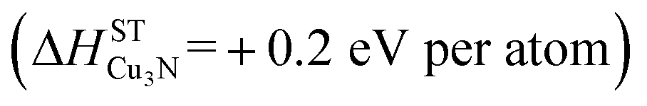 with respect to decomposition into metallic copper solid and molecular nitrogen gas standard reference states:16
| 3Cu (metallic) + 1/2N2 → Cu3N (+0.2 eV per atom) | (1) |
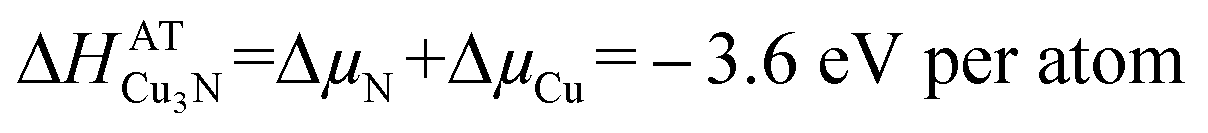
In contrast, Cu3N is stable 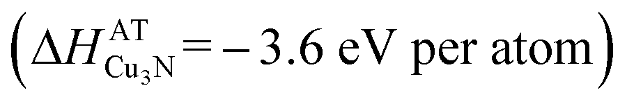 with respect to decomposition into the copper atoms (+3.5 eV per atom with respect to copper solid) and nitrogen atoms (+4.9 eV per atom with respect to molecular nitrogen33) that are used as precursors in the non-equilibrium sputtering process:34
| 3Cu (atoms) + N → Cu3N (−3.6 eV per atom) | (2) |
This difference can be visualized by the energy vs. composition diagram of the copper–nitrogen system shown in Fig. 5. It is notable that the Cu–N ground state line forms a “convex hull”35 with Cu3N at the bottom when referenced to copper atoms and nitrogen atoms, in contrast to the case of Cu solid and N2 gas. This illustrates why it is possible to make metastable Cu3N from sputtered copper atoms and nitrogen atoms despite the positive formation enthalpy of this material with respect to the standard states.
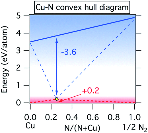 | ||
| Fig. 5 Convex hull diagram for Cu–N system with respect to atomic copper and atomic nitrogen (blue lines) as well as molecular nitrogen and solid copper standard reference states (red lines). | ||
It is possible to use the 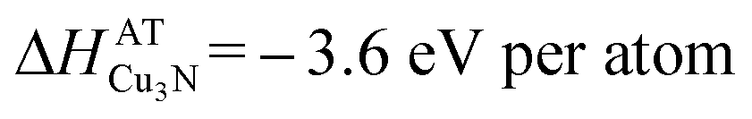 formation enthalpy of Cu3N obtained from the quasi-equilibrium analysis (eqn (1) and (2)) and visualized in Fig. 5 to quantify the effective partial pressure of nitrogen atoms as well as the nitrogen chemical potential as a function of target–substrate distance during the Cu3N growth. The enthalpy of formation of Cu3N is equal to the sum of the chemical potentials of atomic copper (ΔμCu) and atomic nitrogen (ΔμN) as described by:
 | (3) |
In quasi-equilibrium with copper metal (indicated by the dashed line in Fig. 1) ΔμCu = 0 eV per atom and thus from eqn (3) the chemical potential of nitrogen is ΔμN = −3.6 eV per atom. This ΔμN can be written using as:36
ΔμN(T,P) = ΔμoN(T,Po) + kBT![[thin space (1/6-em)]](https://www.rsc.org/images/entities/char_2009.gif) ln(P/Po) ln(P/Po) | (4) |
To determine the range of atomic nitrogen partial pressures, one can solve eqn (3) and (4) knowing from Fig. 1 the temperatures at which Cu3N is in equilibrium with Cu. We find that the pressure varies between 10−31 Torr and 10−26 Torr as the target–substrate distance changes from 13 cm to 15 cm and the equilibrium temperature varies from 150 to 200 °C. Such remarkably small partial pressures of atomic nitrogen required to synthesize copper nitride is the result of large cohesive energy of copper solid and nitrogen molecules (Fig. 5). We note that our effective partial pressure of atomic nitrogen corresponds to the net chemical potential of all nitrogen species present in the discharge.38,39 To assess the highest achievable effective chemical potential of nitrogen for this synthetic technique, we substitute the highest pressure value calculated above (10−26 Torr) and a reasonable expected temperature for a substrate without active heating or cooling (100 °C) back into eqn (4), producing a value of −2.8 eV N−1. This is 2.8 eV N−1 below the atomic Cu to atomic N tie line, and 1 eV N−1above the solid Cu to molecular N2 tie line (Fig. 5). This indicates that metastable binary nitrides that require nitrogen chemical potential of up to +1 eV per atom could potentially be synthesized using reactive sputtering with an atomic nitrogen source. While this limit is likely to be specific for the deposition instrument used in this experiment, the chemical potential limit of any other instrument may be evaluated by finding the maximum temperature at which a known metastable material can be synthesized phase-pure and then following the analysis presented above.
The quasi-thermodynamic analysis presented above provides some insight into the range of the chemical potentials that are achievable by non-equilibrium growth techniques. This insight is important for the computational design of new materials, which has recently attracted significant attention40,41 and has resulted in a few experimental discoveries of previously unreported compounds.42,43 However, a large fraction of materials that are currently being synthesized are thermodynamically unstable.44 Also, it has been recently noted45 that a large number of theoretically predicted useful ternary materials are unstable with respect to competing phases. Referencing these hypothetical non-equilibrium materials to their atomic components, as illustrated in Fig. 5, can be used to evaluate which of them have any chance of being synthetically achievable. Specifically, as illustrated above for the binary metal nitrides it can be expected that metastable materials that require up to +1 eV per atom nitrogen chemical potential should be synthesizable. However, it is important to emphasize that such analysis would provide a necessary but not sufficient metric of synthesizability, because a sufficiently high kinetic barrier to decomposition must also exist to stabilize the non-equilibrium phase. This is likely to be especially important in the case of ternary or more chemically complex compounds where disproportionation into constituent binaries is at least as important as decomposition into elemental phases.
As a first step towards demonstrating the generalizability and predictability of the quasi-thermodynamic analysis for other nitride systems, we selected three metal nitrides (tin nitride, antimony nitride and bismuth nitride) and attempted their synthesis. Tin nitride, Sn3N4, can be used to show the generalizability of our quasi-thermodynamic model. Using the fitted elemental reference energies approach (FERE)46 Sn3N4 has an formation enthalpy of +1.56 eV per formula unit, or about +0.4 eV N−1 with respect to decomposition into Sn metal and N2 gas. Using an analysis similar to Fig. 5 (cohesive energy of tin = 3.1 eV per atom) we obtain a required atomic nitrogen chemical potential of −3.7 eV N−1 for synthesis of this material. At our maximum calculated partial pressure of atomic nitrogen (10−26 Torr) and using eqn (4) we estimate that Sn3N4 should be synthesizable up to 220 °C. This is, as expected, higher than the maximum temperature for the less-stable Cu3N, and should be a good test for the generality of the quasi-thermodynamic chemical potential model. The formation energies and the crystal structures of the two other nitrides, antimony nitride and bismuth nitride, have not been reported in literature, so the maximum temperature of their synthesis is a prediction of their stability relative to Cu3N. The results of investigations of Sn–N, Sb–N and Bi–N are compared to Cu–N in Table 1 and in Fig. S3 of the ESI.†
| Formula | Structure | ΔHf (eV N−1) | T met (°C) |
|---|---|---|---|
| Sn3N4 | Spinel | 0.4 | 450 |
| Cu3N | Anti-ReO3 | 0.8 | 200 |
| SbxNy | Unknown | Unknown | 350 |
| BixNy | Unknown | Unknown | Ambient |
The synthetic results indicate that tin nitride does not start decomposing into Sn and N2 until higher temperatures than Cu3N, qualitatively supporting the quasi-thermodynamic analysis. However the metallic Sn did not precipitate out of Sn3N4 until 450 °C, which is above the 220 °C estimated from the quasi-thermodynamic model. We attribute this difference to the multivalent character of tin (which can be not only in IV+ but also in II+ valence state), since other nitrogen-deficient tin nitride phases were observed at intermediate temperatures. More information about the structure and physical properties of these tin nitrides will be published in the future. Overall, the results for Sn–N are qualitatively consistent with the quasi-thermodynamic model suggesting its generalizability, but more quantitative work on this topic is needed.
Antimony nitride was observed as an amorphous semiconducting film up to 350 °C, and metallic bismuth was the only crystalline phase obtained at ambient substrate temperature. These results indicate that the thermodynamic stability of Sb–N is comparable to that of Sn–N, and that the stability of Bi–N is lower than that of Cu3N. These qualitative predictions require further quantification and call for further experimental and theoretical verification, but they are consistent with the scarce literature on Sb–N and Bi–N materials. For antimony nitride, amorphous semiconducting Sb–N thin films47 and material with an Sb:N = 3:1 composition48 have been reported, suggesting it may have stability similar to Sn–N. In contrast, early reports on bismuth nitride suggest that it is quite reactivive,49,50 and thus likely less thermodynamically stable than Cu3N. More detailed results of the synthesis and stability of Sb–N and Bi–N will be the subject of future publications.
Overall, the results of the Sn–N studies compared to Cu3N indicate that the quasi-thermodynamic analysis may be extendable to other metastable nitride materials, and a first attempt of prediction based on such extension is made for the Sb–N and Bi–N materials, but clearly further research in this area is needed. Once the atomic chemical potential model is fully established, it can be used for predictions of the thermochemistry related quantities that depend on chemical potential (such as defect formation energies and charge carrier concentrations) for both metastable and stable nitrides. If successful, such an approach may also be generalizable to other anions such as O, F, or S in the future.
Conclusions
In summary, we report the synthesis and semiconducting properties of metastable copper nitride thin films prepared using reactive sputtering. Phase pure Cu3N thin films were synthesized in the presence of a nitrogen atom source using a high-throughput combinatorial approach with orthogonal gradients of target–substrate distance and substrate temperature, both affecting the nitrogen activity. In turn, the nitrogen activity influences both the phase purity and the morphology of the resulting Cu3N thin films. This high-throughput synthesis technique is a valuable contribution to combinatorial materials science, which up to date has focused primarily on cation gradients. The phase pure 00L oriented Cu3N thin films have conductivities of 10−3 S cm−1 and a 1.4–1.6 eV optical absorption onset. These results indicate that Cu3N may be a promising candidate for solar cell absorber applications, calling for more detailed studies on this topic. Additionally, we report the quasi-thermodynamic chemical potential model for the synthesis of Cu3N, which explains the sputtering growth of this metastable material by referencing it to its atomic (Cu and N) rather than standard (Cu solid and N2 gas) reference states. Using this model, we estimate that at least +1 eV per atom effective nitrogen chemical potential is achievable in the process of reactive sputtering with a nitrogen atom source. This result, and the underlying quasi-thermodynamic model, may be generalizable to theoretical prediction and experimental synthesis of other metastable materials as exemplified for the nitrides of antimony, tin, and bismuth.Acknowledgements
This research is supported by the U.S. Department of Energy, office of Energy Efficiency and Renewable Energy, as a part of the “Ternary Copper Nitride Absorbers” Next Generation PV II project within the SunShot initiative. The authors would like to thank John D. Perkins, Stephan Lany, Vladan Stevanović and Julien Vidal for illuminating discussions and Sn3N4 FERE calculations.Notes and references
- L. Maya, J. Vac. Sci. Technol., A, 1993, 11, 604–608 CAS.
- T. Maruyama and T. Morishita, J. Appl. Phys., 1996, 69, 890–891 CAS.
- R. Cremer, M. Witthaut, D. Neusch, C. Trappe, M. Laurenzis, O. Winker and H. Kurz, Mikrochim. Acta, 2000, 133, 299–302 CrossRef CAS.
- D. M. Borsa, S. Grachev, C. Presura and D. O. Boerma, Appl. Phys. Lett., 2002, 80, 1823–1825 CrossRef CAS PubMed.
- W. Zhu, X. Zhang, X. Fu, Y. Zhou, S. Luo, X. Wu, I. Resistive and T. Cu, Phys. Status Solidi A, 2012, 1–6 Search PubMed.
- J. F. Pierson, Vacuum, 2002, 66, 59–64 CrossRef CAS.
- N. Gordillo, R. Gonzalez-Arrabal, M. S. Martin-Gonzalez, J. Olivares, A. Rivera and F. Briones, J. Cryst. Growth, 2008, 310, 4362–4367 CrossRef CAS PubMed.
- N. Gordillo, R. Gonzalez-Arrabal, P. Diaz-Chao, J. R. Ares, I. J. Ferrer, F. Yndurain and F. Agulló-López, Thin Solid Films, 2013, 531, 588–591 CrossRef CAS PubMed.
- A. L. Ã. Ji, R. Huang, Y. Du, C. R. Li, Y. Q. Wang and Z. X. Cao, J. Cryst. Growth, 2006, 295, 79–83 CrossRef CAS PubMed.
- T. Maruyama and T. Morishita, J. Appl. Phys., 1995, 78, 1–5 CrossRef PubMed.
- T. Nosaka, M. Yoshitake, A. Okamoto and S. Ogawa, Thin Solid Films, 1999, 348, 8–13 CrossRef CAS.
- J.-L. Bredas, Mater. Horiz., 2014, 1, 17 RSC.
- F. Hadian, A. Rahmati, H. Movla and M. Khaksar, Vacuum, 2012, 86, 1067–1072 CrossRef CAS PubMed.
- M. Yang, A. Zakutayev, J. Vidal, X. Zhang, D. S. Ginley and F. J. DiSalvo, Energy Environ. Sci., 2013, 6, 2994 CAS.
- A. Zakutayev, C. M. Caskey, A. N. Fioretti, D. S. Ginley, J. Vidal, V. Stevanović, E. Tea and S. Lany, J. Phys. Chem. Lett., 2014, 5, 1117–1125 CrossRef CAS.
- S. Lany, Phys. Rev. B: Condens. Matter Mater. Phys., 2008, 78, 245207 CrossRef.
- Z. Q. Liu, W. J. Wang, T. M. Wang, S. Chao and S. K. Zheng, Thin Solid Films, 1998, 325, 55–59 CrossRef CAS.
- J. F. Pierson, D. Wiederkehr and A. Billard, Thin Solid Films, 2005, 478, 196–205 CrossRef CAS PubMed.
- G. H. Yue, P. X. Yan and J. Wang, J. Cryst. Growth, 2005, 274, 464–468 CrossRef CAS PubMed.
- M. L. Green, I. Takeuchi and J. R. Hattrick-Simpers, J. Appl. Phys., 2013, 113, 231101 CrossRef PubMed.
- A. Zakutayev, F. J. Luciano, V. P. Bollinger, A. K. Sigdel, P. F. Ndione, J. D. Perkins, J. J. Berry, P. a. Parilla and D. S. Ginley, Rev. Sci. Instrum., 2013, 84, 053905 CrossRef PubMed.
- I. Takeuchi, R. B. van Dover and H. Koinuma, MRS Bull., 2002, 301–308 CrossRef CAS.
- A. Zakutayev, T. R. Paudel, P. F. Ndione, J. D. Perkins, S. Lany, A. Zunger and D. S. Ginley, Phys. Rev. B: Condens. Matter Mater. Phys., 2012, 85, 085204 CrossRef.
- H. Koinuma and I. Takeuchi, Nat. Mater., 2004, 3, 429–438 CrossRef CAS PubMed.
- A. Zakutayev, J. D. Perkins, P. A. Parilla, N. E. Widjonarko, A. K. Sigdel, J. J. Berry and D. S. Ginley, MRS Commun., 2011, 1, 23–26 CrossRef CAS.
- V. Cloet, A. Raw, K. R. Poeppelmeier, G. Trimarchi, H. Peng, J. Im, A. J. Freeman, N. H. Perry, T. O. Mason, A. Zakutayev, P. F. Ndione, D. S. Ginley and J. D. Perkins, Chem. Mater., 2012, 24, 3346–3354 CrossRef CAS.
- T. Chikyow, P. Ahmet, K. Nakajima, T. Koida, M. Takakura, M. Yoshimoto and H. Koinuma, Appl. Surf. Sci., 2002, 189, 284–291 CrossRef CAS.
- A. Zakutayev, N. H. Perry, T. O. Mason, D. S. Ginley and S. Lany, Appl. Phys. Lett., 2013, 103, 232106 CrossRef PubMed.
- T. Koida, D. Komiyama, H. Koinuma, M. Ohtani, M. Lippmaa and M. Kawasaki, Appl. Phys. Lett., 2002, 80, 565 CrossRef CAS PubMed.
- A. Submaraniyan, J. D. Perkins, R. P. O'Hayre, S. Lany, V. Stephanovic, D. S. Ginley and A. Zakutayev, APL Mater., 2014, 2, 022105 CrossRef PubMed.
- S. Ohashi, M. Lippmaa, N. Nakagawa, H. Nagasawa, H. Koinuma and M. Kawasaki, Rev. Sci. Instrum., 1999, 70, 178 CrossRef CAS PubMed.
- Y. Du, A. L. Ã. Ji, L. B. Ma, Y. Q. Wang and Z. X. Cao, J. Cryst. Growth, 2005, 280, 490–494 CrossRef CAS PubMed.
- B. deB. Darwent, Bond Dissociation Energies in Simple Molecules, National Standard Reference Data System, National Bureau of Standards, United States, 1970 Search PubMed.
- I. Petrov, A. Myers, J. E. Greene and J. R. Abelson, J. Vac. Sci. Technol., A, 2012, 2846, 2846–2854 Search PubMed.
- S. Wei, L. Ferreira and A. Zunger, Phys. Rev. B: Condens. Matter Mater. Phys., 1990, 41, 8240–8269 CrossRef CAS.
- K. Reuter and M. Scheffler, Phys. Rev. B: Condens. Matter Mater. Phys., 2001, 65, 1–11 CrossRef.
- M. W. J. Chase, NIST Web B., 1998 Search PubMed.
- A. J. Ptak, K. S. Ziemer, M. R. Millecchia, C. D. Stinespring and T. H. Myers, MRS Internet J. Nitride Semicond. Res., 1999, 4S1, 1–6 Search PubMed.
- W. E. Hoke, P. J. Lemonias and D. G. Weir, J. Cryst. Growth, 1991, 111, 1024–1028 CrossRef CAS.
- B. Meredig and C. Wolverton, Nat. Mater., 2013, 12, 123–127 CrossRef CAS PubMed.
- S. Curtarolo, G. L. W. Hart, M. B. Nardelli, N. Mingo, S. Sanvito and O. Levy, Nat. Mater., 2013, 12, 191–201 CrossRef CAS PubMed.
- A. Zakutayev, X. Zhang, A. Nagaraja, L. Yu, S. Lany, T. O. Mason, D. S. Ginley and A. Zunger, J. Am. Chem. Soc., 2013, 135, 10048–10054 CrossRef CAS PubMed.
- G. Hautier, A. Jain and S. P. Ong, J. Mater. Sci., 2012, 47, 7317–7340 CrossRef CAS.
- J. E. Saal, S. Kirklin, M. Aykol, B. Meredig and C. Wolverton, JOM, 2013, 65, 1501–1509 CrossRef CAS PubMed.
- X. Zhang, L. Yu, A. Zakutayev and A. Zunger, Adv. Funct. Mater., 2012, 22, 1425–1435 CrossRef CAS.
- V. Stevanović, S. Lany, X. Zhang and A. Zunger, Phys. Rev. B: Condens. Matter Mater. Phys., 2012, 85, 115104 CrossRef.
- T. Shiraishi, A. Yasuyuki and S. Yamazaki, J. Non-Cryst. Solids, 1985, 77–78, 1313–1316 CrossRef CAS.
- Q. Sun, W.-J. Li and Z.-W. Fu, Solid State Sci., 2010, 12, 397–403 CrossRef CAS PubMed.
- I. Schrman and W. C. Fernelius, J. Am. Chem. Soc., 1930, 52, 2425–2430 CrossRef.
- E. C. Franklin, J. Am. Chem. Soc., 1905, 836, 820–851 CrossRef.
Footnote |
| † Electronic supplementary information (ESI) available: More detailed experimental methods and a comparison of films grown with and without the atomic nitrogen source and at different target powers is available. A reformatted version of Fig. 3 is presented. Additionally, XRD patterns from the investigations of tin, antimony, and bismuth systems are included. See DOI: 10.1039/c4mh00049h |
| This journal is © The Royal Society of Chemistry 2014 |