High performance photocatalytic metal oxide synthetic bi-component nanosheets formed by atomic layer deposition†
Kyoungmi
Lee
,
Mark D.
Losego
,
Do Han
Kim
and
Gregory N.
Parsons
*
Department of Chemical and Biomolecular Engineering, North Carolina State University, Raleigh, North Carolina 27695, USA. E-mail: parsons@ncsu.edu
First published on 18th March 2014
Abstract
Synthetic nanosheets that are ultrathin variants of bulk materials have been acquired using atomic layer deposition (ALD) on dissolvable substrates with a control over layer dimension including single and bilayered “Janus nanosheet” structures. TiO2, ZnO, Al2O3 and TiO2/ZnO nanosheets function as dispersible photocatalysts in aqueous media showing 3× synergistic rate enhancement for bilayered nanosheets.
Two-dimensional nanosheet materials, including graphene, MoS2, perovskites, and others derived from naturally occurring bulk layered compounds show unique electrical and mechanical functionality.1–12 They are typically formed by mechanical or chemical exfoliation from bulk materials,11,12 or by vapor-phase or hydrothermal growth in morphologically constrained systems.13,14 Structures are generally limited to single-compound systems with limited control over layer dimension.
Here we present a new strategy for synthesizing 2D nanosheets, including single and multi-compound structures, using atomic layer deposition (ALD) on dissolvable substrates. ALD uses a binary self-limiting reaction sequence to precisely control thin film nucleation and growth at the monolayer level15,16 and enables formation of gradual or abrupt material junctions by adjusting the precursor exposure sequence in successive ALD cycles. ALD films are known to enhance performance of batteries,17,18 capacitors,19 and transistor devices.20,21
While ALD thin film materials and coatings are well-known in electronic device manufacturing,21,22 we hypothesize that controlled ALD on solution-soluble substrates could expand the known benefits of ALD to create free-floating 2D materials without the constraint of a substrate, capable of functional performance analogous to natural nanosheets. The synthetic nanosheets formed by ALD are distinct from exfoliated natural nanosheets in that they are ultrathin variants of bulk materials, and they are not inherently layered. The rationale for exploring the ALD method is that it presents synthetic options not available in homogeneously prepared or commercial powder structures. Specifically, ALD allows for readily controlled thickness, surface area and material composition. ALD also allows multi-component layering which permits electronic structuring and modified optical response not available in other laboratory or commercial materials. As an example application, we show that ALD can be used to synthesize TiO2, ZnO, Al2O3 and TiO2/ZnO bilayered nanosheets that function as dispersible photocatalysts in aqueous media.
The overall procedure for ALD synthetic nanosheet production is presented in Fig. 1. Sacrificial layers of water soluble polymers were spun-cast onto Si substrates with native SiO2 (Fig. 1a). We choose polyvinyl alcohol (PVA) and polyacrylic acid (PAA) for sacrificial layers because of their ability to promote ALD metal oxide nucleation23 and their high water solubility.24 Films of controlled thickness and composition were then deposited by ALD onto the sacrificial polymer layer (Fig. 1b). To facilitate dissolution of the sacrificial layer, surfaces were pre-cut by hand with a razor (Fig. 1c). Sacrificial layers were dissolved in deionized (DI) water heated to ∼60 °C. After several minutes (1–5 min), nanosheets with lateral sizes up to ∼3 mm were released into solution (Fig. 1d). For structural analysis, nanosheets were collected on clean silicon wafers for atomic force microscopy (AFM) analysis or on molybdenum grids for transmission electron microscopy (TEM) imaging (see ESI† for detailed experimental procedure).
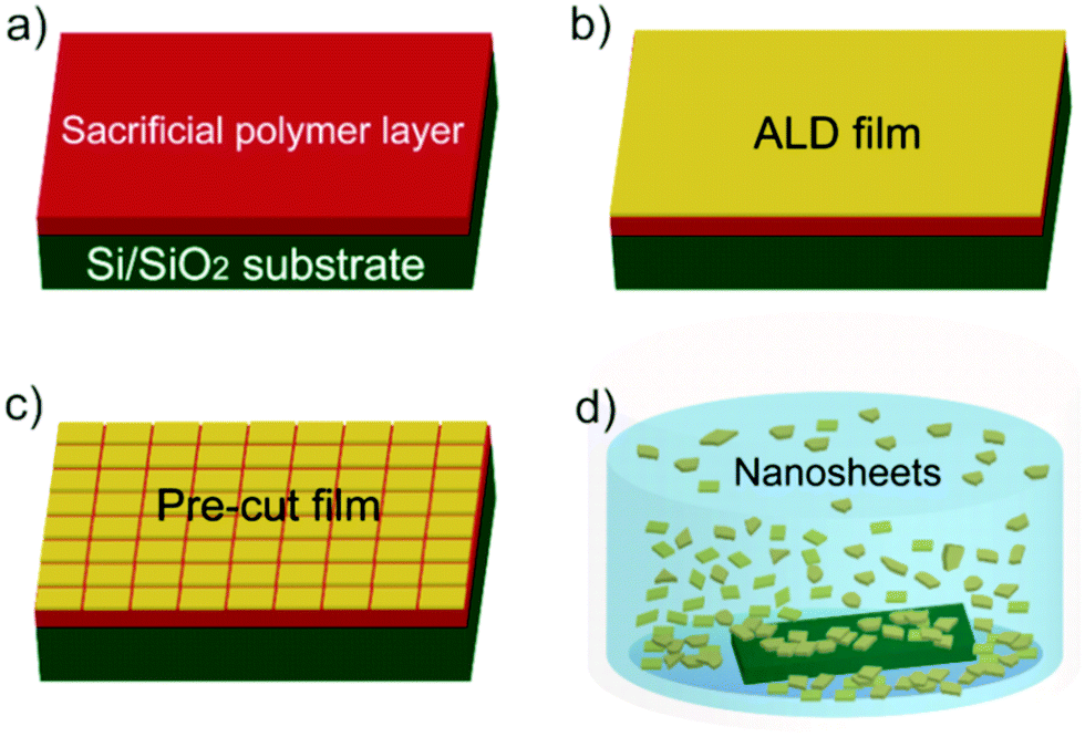 | ||
| Fig. 1 Fabrication of synthetic ALD nanosheets. (a) A 2 wt% polymer solution was spin-coated on Si substrate as a sacrificial layer. (b) Metal oxide ALD was performed onto the polymer layer with desired thickness and materials. (c) Pre-cuts were made into the polymer surface to facilitate dissolution of the polymer. (d) The polymer was removed by dipping in a solvent and ALD films were separated as nanosheets randomly dispersed in aqueous solution. | ||
Fig. 2 summarizes how the ALD process provides high fidelity control over nanosheet thickness and morphology. Fig. 2a illustrates that TiO2 nanosheet thickness, measured by ellipsometry and AFM, varies linearly with the number of ALD growth cycles. AFM profiles of released nanosheet thickness precisely match ellipsometry measurements collected from control films grown directly on silicon wafers. Fig. 2b–d show AFM images collected from TiO2, Al2O3, and ZnO nanosheets respectively. These AFM scans are collected at the minimum thickness for each composition formed under the conditions used. Below this thickness, the ALD layers tend to break apart into nanosheets with smaller lateral dimension. The nanosheet thickness obtained by AFM was very repeatable (typically <±5%) from run-to-run. For this series of ALD precursor chemistries on PAA or PVA sacrificial layers, TiO2 exhibits the smallest layer thickness (∼1.2 nm), corresponding to a length-to-thickness ratio of >20![[thin space (1/6-em)]](https://www.rsc.org/images/entities/char_2009.gif) 000.
000.
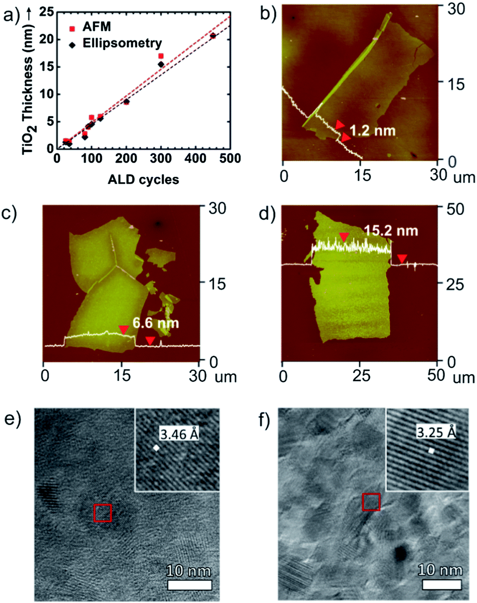 | ||
| Fig. 2 (a) Graph of TiO2 nanosheet thickness collected from AFM height profiles (squares) and from ellipsometry (diamonds) as a function of the number of ALD cycles. AFM images and height profiles of (b) TiO2 nanosheets from 25 ALD cycles, (c) Al2O3 nanosheets from 50 ALD cycles, and (d) ZnO nanosheet from 100 ALD cycles. These micrographs show the minimum nanosheet thickness achieved for each material. (e) TEM image of TiO2 nanosheet annealed at 450 °C for 1 h. (f) TEM image of ZnO nanosheet annealed at 300 °C for 1 h. Magnified inset images obtained from the red areas show the lattice parameter for each material. | ||
After formation by low-temperature ALD, TiO2 and ZnO films are known to be amorphous and polycrystalline, respectively. We are interested in the function of as-prepared nanosheets without the need for further processing. However some samples were annealed to examine the crystal habit and extent of crystallization of these structures. Nanosheets collected on molybdenum grids were annealed to 450 °C for TiO2 and 300 °C for ZnO. TEM micrographs of these crystallized nanosheets are shown in Fig. 2e and f. In these images the thickness of the TiO2 nanosheet is ∼7.0 nm and the thickness of the ZnO nanosheet is ∼17.3 nm. In Fig. 2e, the TiO2 nanosheet exhibits a lattice spacing of 3.46 Å, which corresponds to the a lattice parameter of the anatase phase of TiO2.25 The ZnO nanosheet (Fig. 2f) shows a lattice spacing of 3.25 Å which matches the a lattice parameter for the wurtzite phase of ZnO.26 The diffraction patterns for TiO2 and ZnO nanosheets are shown in Fig. S1.† After being annealed, TiO2 nanosheet has polycrystalline (Fig. S1a†) and single-crystalline (Fig. S1b†) which are obtained from light gray and dark gray domains in Fig. 2e. Also, the diffraction pattern of ZnO nanosheet shows that it is mostly polycrystalline with sharp rings (Fig. S1c†).
Besides single phase nanosheets, multicomponent and layered nanosheet structures can be designed by alternating ALD chemistries. As an example, we have prepared bilayer nanosheets composed of TiO2 and ZnO. Fig. 3a shows the deposition scheme for these ALD nanosheet bilayers. In this experiment, PVA sacrificial layers were initially coated with ALD ZnO (150 cycles) followed by ALD TiO2 (500 cycles). Because of the low deposition temperature, mixing between the TiO2 and ZnO layer will be minimal. The inset in Fig. 3b shows a scanning electron microscopy (SEM) image of a ZnO/TiO2 bilayer nanosheet transferred to a silicon substrate. Energy dispersive X-ray analysis (EDX) indicates the presence of Zn, Ti, and O, confirming that these bilayer structures remain intact after being released from the sacrificial polymer. An AFM image of a similar nanosheet is shown in Fig. 3c, and Fig. 3d shows a set of dispersed nanosheets in water. The AFM image shows the thickness is 36.9 nm where some double or triple layers result from nanosheet folding when it is collected on the planar substrate.
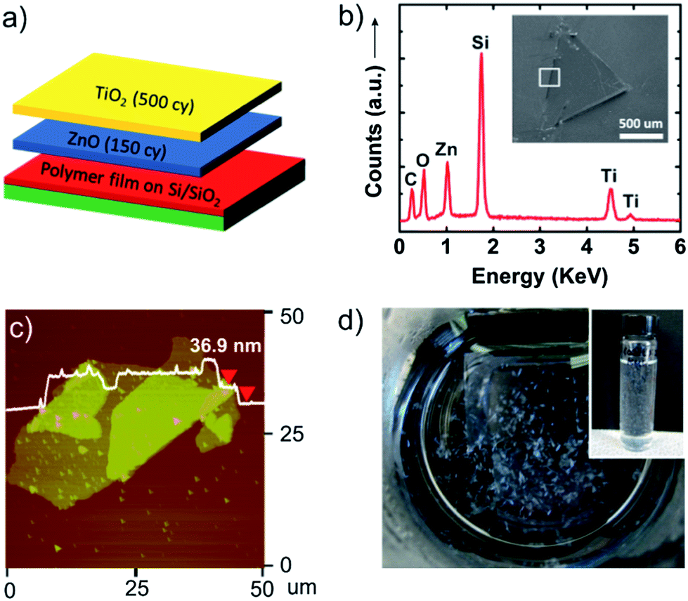 | ||
| Fig. 3 (a) Illustration showing deposition order and the number of ALD cycles for the ZnO/TiO2 bilayer film. (b) EDX spectrum taken from the edge of the bilayer nanosheet shown in the inset SEM image. (c) AFM image and height profile of the bilayer nanosheet. (d) Picture of TO2/ZnO bilayer nanosheets dispersed in DI water and nanosheets collected in a vial (inset). | ||
Many oxide nanomaterials can function as photocatalysts to degrade volatile organic pollutants and purify air or water.27 Recently, multicomponent nanomaterials including TiO2 with graphene,28 TiO2 nanofibers with ZnO,29 and TiO2 nanoparticles with carbon nanotubes30 have shown improved performance relative to pure nano-TiO2 evaluated under the same conditions. Improvements are typically associated with increased adsorption of organic species on the compound surface, extended range of photon absorption, and improved charge separation and transfer to the reacting species. The unique ability to control material thickness and synthesize bi-component compound nanosheets by ALD could provide new flexibility in photocatalyst materials design and preparation. Therefore, we have explored the photocatalytic performance of our TiO2, ZnO, and TiO2/ZnO bilayer ALD nanosheets in aqueous solution, including the scaling of photocatalytic rate processes with changing nanosheet thickness, surface area and electronic structure. We compare our experimental results to a standard analytical reaction model. For photocatalytic experiments, ALD films on a sacrificial layer were directly released in DI water during polymer dissolution and examined without annealing. Although nanosheets are expected to have crystalline and amorphous phases without annealing, they still have photocatalytic activity.31,32
Compared to a single layer on a flat substrate, nanosheets with the same total area released into solution will enhance performance by enabling solution contact with both the front and back surfaces. Also, the nanosheet thickness can be much less than the photon penetration depth, so at high nanosheet concentrations, multiple nanosheets can be in the photo-pathway, increasing scattering and the overall photon absorption.
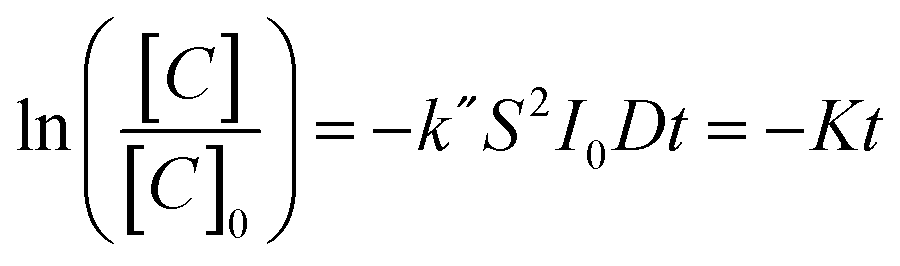
Here we use methyl orange as a prototypical pollutant. The derivation of the methyl orange photo-decomposition rate expression can be found in the ESI.† The methyl orange concentration will scale as a log-linear function of irradiation time:
 | (1) |
Fig. 4a shows the concentration of methyl orange as a function of UV exposure time in the presence of TiO2 nanosheets using thickness values fixed between 1.3 and 5.0 nm. The total nanosheet surface area was 160 cm2 and the UV flux was set at 245 μW cm−2. All samples show dye absorbance loss upon UV exposure, with an increased rate of loss with increasing nanosheet thickness. From [eqn (1)], the slopes of the linear fits in Fig. 4a are a measure for K = k′′S2I0D, and Fig. 4b is a plot of K (from Fig. 4a) versus film thickness. K increases linearly with film thickness, as expected from [eqn (1)]. This result reflects the expected mechanistic trend where thicker nanosheets will absorb more photons and thereby boost the number of oxidizing species created. Since the diffusion length of photogenerated carriers in polycrystalline TiO2 is at least ∼1 μm, we expect all charges to reach the surface in our thin nanosheets.33 Using known values for S and I0 the linear fit in Fig. 4b gives k′′ ≈ 4.2 × 10⁻¹¹ s−1 cm−2 μW−1 nm−1. We note that the K value for the thinnest nanosheets (1.3 nm) falls below the trend line. This may be experimental uncertainty or it may reflect quantum confinement that would tend to increase the bandgap and reduce photoabsorption.34–36
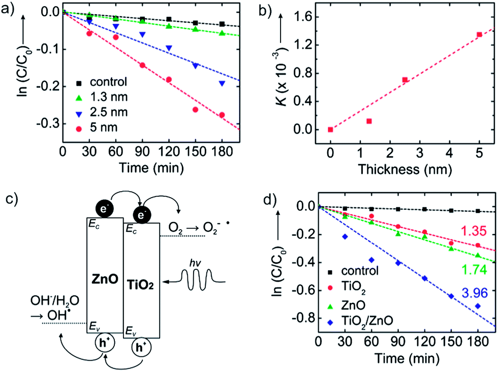 | ||
| Fig. 4 (a) The concentration of methyl orange versus UV exposure time onto TiO2 nanosheets of various thickness (1.3, 2.5, and 5 nm). Black squares show the control data for methyl orange concentration versus time without nanosheets present. (b) Plot of apparent rate constants (K) versus surface area extracted from the data shown in (a). (c) Schematic band energy diagram of TiO2/ZnO bilayer nanosheets. The band offset promotes migration of photogenerated holes to the ZnO and electrons to the TiO2 layer, limiting recombination and enhancing photocatalytic performance. Also shown are the relative electrochemical potentials for oxygen reduction to superoxide and water oxidation to hydroxyl radicals. (d) Photodegradation of methyl orange with UV-irradiation time with no nanosheets (control, black squares), TiO2 nanosheets (red circles), ZnO nanosheets (green triangles), and ZnO/TiO2 bilayer nanosheets (blue diamonds). All nanosheets have thickness ∼5 nm and surface area of 160 cm.2 Each number represents K (×10−3 min−1). | ||
Dye decomposition rate data was also collected by irradiating TiO2 nanosheet dispersions using various UV intensity values and nanosheet surface areas keeping other parameters fixed. Plots of ln(C/C0) vs. time follow [eqn (1)] (Fig. S2a†). Using S = 160 cm2, a plot of K vs. I0 is linear with k′′ ≈ 3.8 × 10⁻¹¹ s−1 cm−2 μW−1 nm−1, essentially the same k′′ value as from Fig. 4b (Fig. S2b†). Increasing the surface area (by increasing nanosheet concentration) also affects the value of K. However, at high S (i.e., high nanosheet concentrations) we expect light scattering to decrease the photon flux on nanosheets deeper in solution. Using different S values, dye decomposition rate was measured using fixed D and I0, and values for k′′ were obtained for each condition (Fig. S3a and b†). We find larger values for k′′ for smaller values of S as expected from the model trend. Larger concentrations of nanosheets scatter light more strongly, decreasing the net photon flux on nanosheets deeper in the solution, thereby decreasing the effective rate of dye degradation, k′′ (Fig. S3c†).
A distinctive aspect of ALD nanosheet synthesis is its facile ability to create compositional bilayers with controlled thickness of each layer. Based on the two materials' difference in band energy levels,37,38 a TiO2/ZnO bilayer structure will separate photogenerated electrons and holes as depicted in Fig. 4c. The redox reactions at each surface are thermodynamically favorable when considered their potential.39 The bilayer will also spatially separate the oxidation and reduction reactions to different sides of the nanosheet, helping to increase overall reaction rates. While some charge trapping and recombination could be expected at the bilayer interface, the relatively abrupt junction formed by low temperature ALD will promote charge separation and increase the rate of photo-catalytic degradation relative to the single-component materials. Unlike other bi-component photocatalysts, our bilayer nanosheets consist of two distinct material layers, with the structure of a planar ‘Janus nanosheet’.40,41Fig. 4d plots methyl orange photodegradation using TiO2, ZnO, and TiO2/ZnO nanosheets with a thickness of 5 nm and a surface area of 160 cm2. The K values extracted from these and other related degradation measurements are presented in Table 1. The ZnO nanosheets lead to modestly (∼25%) faster organic photodegradation than TiO2. Consistent with [eqn (1)], the value of K increases linearly with nanosheet thickness.
| Nanosheet material | Thickness (nm) | K (×10−3 min−1) |
|---|---|---|
| TiO2 | 2.5 | 0.71 |
| TiO2 | 5 | 1.35 |
| ZnO | 5 | 1.74 |
| TiO2/ZnO | 2.5/2.5 | 3.96 |
To analyze the photocatalytic response of the bilayer (TiO2/ZnO = 2.5/2.5 nm) catalyst, we compared it to ∼5 nm thick single-component TiO2 or ZnO nanosheets which, considering the ZnO and TiO2 densities, will have nearly the same mass (within ∼20%) as the bilayer sheets. We find that the bilayer nanosheet degrades the dye ∼3× faster than 5 nm thick TiO2 and ∼2.3× faster than or 5 nm thick ZnO nanosheets. The bilayer degrades the dye >5.5× faster than the 2.5 nm thick single-component TiO2 nanosheet without the ZnO layer present. The rate enhancement for the bilayer is ascribed to charge separation at the ZnO/TiO2 interface, where photogenerated electrons and holes move into the TiO2 and ZnO layers, respectively. Even though the bilayer structure was not optimized for relative performance, the measured rate enhancement is noteworthy when compared to other bi-component photocatalysts. For example, TiO2/ZnO nanofibers29 and Ag/TiO2/ZnO composite particles42 show rate enhancements up to 2× faster than for TiO2 alone. Also, adding carbon nanotubes30,43 or graphene28 can enhance the rate, but improvements are limited to ∼2.5× better than TiO2 alone. While overall performance enhancement will depend on the base starting material, the ∼3× rate enhancement we observe for the bilayer TiO2/ZnO ALD nanosheets compared to the TiO2 alone is notable in comparison to previous reports of performance enhancement for bi-component structures relative to TiO2.
We hypothesize that the physical symmetry of our bilayer structures contributes to the enhanced synergistic photodecomposition rates. Synthesis of most bi-component particles provides only modest control over size, shape, surface area and net amount of each component material. Our synthetic nanosheets have high surface-to-volume ratios (1.5–0.4 nm−1 for 1.3–5 nm thickness, respectively), compositional symmetry, and individual layer thickness control to ensure that active redox species can readily access active surface sites, helping to balance the extent of the complementary surface oxidation and reduction reactions.
In summary, we have shown how ALD thin film reactions can produce synthetic metal oxide nanosheets with precisely controlled thickness and aspect ratios of >20000:1. Single component nanosheets composed of TiO2 and ZnO exhibit photocatalytic activity, and the catalytic dye decomposition rate scales as expected with photodecomposition kinetic rate equations developed for the nanosheet structures. Photocatalytic decomposition rates are significantly boosted using ZnO/TiO2 bilayer nanosheets, and the synergistic rate enhancement is larger than previously reported for other bi-component photocatalyst materials. The ALD synthesis process is unique in that it yields physically symmetric nanosheets, and the symmetry likely helps balance redox rates and thereby assists in achieving high performance. ALD also enables multi-component nanosheet junctions which modulate the nanosheet electronic band structure and synergistically enhance the rate of photocatalytic pollutant degradation. The addition of sensitizing dyes or catalytic sites before release could further expand nanosheet functionality and performance. These initial demonstrations of functional synthetic nanosheets by ALD suggest that a much broader set of materials, including metals, semiconductors, ceramics, organics and organic–inorganic hybrid materials could be produced in nanosheet form and evaluated for catalytic or other useful functions.
Acknowledgements
We appreciate the financial support by NSF (CBET-1034374).Notes and references
- K. S. Novoselov, A. K. Geim, S. V. Morozov, D. Jiang, Y. Zhang, S. V. Dubonos, I. V. Grigorieva and A. A. Firsov, Science, 2004, 306, 666–669 CrossRef CAS PubMed.
- A. K. Geim and K. S. Novoselov, Nat. Mater., 2007, 6, 183–191 CrossRef CAS PubMed.
- T. Sasaki, M. Watanabe, H. Hashizume, H. Yamada and H. Nakazawa, J. Am. Chem. Soc., 1996, 118, 8329–8335 CrossRef CAS.
- Y. Omomo, T. Sasaki, L. Z. Wang and M. Watanabe, J. Am. Chem. Soc., 2003, 125, 3568–3575 CrossRef CAS PubMed.
- J. N. Coleman, M. Lotya, A. O'Neill, S. D. Bergin, P. J. King, U. Khan, K. Young, A. Gaucher, S. De, R. J. Smith, I. V. Shvets, S. K. Arora, G. Stanton, H. Y. Kim, K. Lee, G. T. Kim, G. S. Duesberg, T. Hallam, J. J. Boland, J. J. Wang, J. F. Donegan, J. C. Grunlan, G. Moriarty, A. Shmeliov, R. J. Nicholls, J. M. Perkins, E. M. Grieveson, K. Theuwissen, D. W. McComb, P. D. Nellist and V. Nicolosi, Science, 2011, 331, 568–571 CrossRef CAS PubMed.
- B. Radisavljevic, A. Radenovic, J. Brivio, V. Giacometti and A. Kis, Nat. Nanotechnol., 2011, 6, 147–150 CrossRef CAS PubMed.
- C. Schliehe, B. H. Juarez, M. Pelletier, S. Jander, D. Greshnykh, M. Nagel, A. Meyer, S. Foerster, A. Kornowski, C. Klinke and H. Weller, Science, 2010, 329, 550–553 CrossRef CAS PubMed.
- J. Feng, L. L. Peng, C. Z. Wu, X. Sun, S. L. Hu, C. W. Lin, J. Dai, J. L. Yang and Y. Xie, Adv. Mater., 2012, 24, 1969–1974 CrossRef CAS PubMed.
- Y. Ebina, T. Sasaki, M. Harada and M. Watanabe, Chem. Mater., 2002, 14, 4390–4395 CrossRef CAS.
- S. Ida, C. Ogata, M. Eguchi, W. J. Youngblood, T. E. Mallouk and Y. Matsumoto, J. Am. Chem. Soc., 2008, 130, 7052–7059 CrossRef CAS PubMed.
- M. Osada and T. Sasaki, J. Mater. Chem., 2009, 19, 2503–2511 RSC.
- Y. Ebina, N. Sakai and T. Sasaki, J. Phys. Chem. B, 2005, 109, 17212–17216 CrossRef CAS PubMed.
- S. J. Chen, Y. C. Liu, C. L. Shao, R. Mu, Y. M. Lu, J. Y. Zhang, D. Z. Shen and X. W. Fan, Adv. Mater., 2005, 17, 586–590 CrossRef CAS.
- J. Q. Hu, Y. Bando, J. H. Zhan, Y. B. Li and T. Sekiguchi, Appl. Phys. Lett., 2003, 83, 4414–4416 CrossRef CAS PubMed.
- V. Miikkulainen, M. Leskela, M. Ritala and R. L. Puurunen, J. Appl. Phys., 2013, 113, 021301 CrossRef PubMed.
- G. N. Parsons, S. M. George and M. Knez, MRS Bull., 2011, 36, 865–871 CrossRef CAS.
- Y. S. Jung, A. S. Cavanagh, L. A. Riley, S. H. Kang, A. C. Dillon, M. D. Groner, S. M. George and S. H. Lee, Adv. Mater., 2010, 22, 2172–2176 CrossRef CAS PubMed.
- X. Zhang, I. Belharouak, L. Li, Y. Lei, J. W. Elam, A. Nie, X. Chen, R. S. Yassar and R. L. Axelbaum, Adv. Energy Mater., 2013, 3, 1299–1307 CrossRef CAS.
- X. Yu, C. Zhu, H. Hu, A. Chin, M.-F. Li, B. Jin Cho, D.-L. Kwong, P. Foo and M. B. Yu, IEEE Electron Device Lett., 2003, 24, 63–65 CrossRef CAS.
- B.-Y. Oh, Y.-H. Kim, H.-J. Lee, B.-Y. Kim, H.-G. Park, J.-W. Han, G.-S. Heo, T.-W. Kim, K.-Y. Kim and D.-S. Seo, Semicond. Sci. Technol., 2011, 26, 085007 CrossRef.
- H. Liu and P. D. Ye, IEEE Electron Device Lett., 2012, 33, 546–548 CrossRef CAS.
- L. Niinistö, M. Nieminen, J. Päiväsaari, J. Niinistö and M. Putkonen, Phys. Status Solidi A, 2004, 201, 1443–1452 CrossRef.
- Q. Peng, X. Y. Sun, J. C. Spagnola, G. K. Hyde, R. J. Spontak and G. N. Parsons, Nano Lett., 2007, 7, 719–722 CrossRef CAS PubMed.
- V. Linder, B. D. Gates, D. Ryan, B. A. Parviz and G. M. Whitesides, Small, 2005, 1, 730–736 CrossRef CAS PubMed.
- R. Asahi, Y. Taga, W. Mannstadt and A. J. Freeman, Phys. Rev. B: Condens. Matter Mater. Phys., 2000, 61, 7459–7465 CrossRef CAS.
- Z. W. Pan, Z. R. Dai and Z. L. Wang, Science, 2001, 291, 1947–1949 CrossRef CAS PubMed.
- U. I. Gaya and A. H. Abdullah, J. Photochem. Photobiol., C, 2008, 9, 1–12 CrossRef CAS PubMed.
- Y. H. Zhang, Z. R. Tang, X. Z. Fu and Y. J. Xu, ACS Nano, 2010, 4, 7303–7314 CrossRef CAS PubMed.
- R. L. Liu, H. Y. Ye, X. P. Xiong and H. Q. Liu, Mater. Chem. Phys., 2010, 121, 432–439 CrossRef CAS PubMed.
- Y. Yu, J. C. Yu, C. Y. Chan, Y. K. Che, J. C. Zhao, L. Ding, W. K. Ge and P. K. Wong, Appl. Catal., B, 2005, 61, 1–11 CrossRef CAS PubMed.
- S.-M. Lee, G. Grass, G.-M. Kim, C. Dresbach, L. Zhang, U. Gösele and M. Knez, Phys. Chem. Chem. Phys., 2009, 11, 3608–3614 RSC.
- B. Ohtani, Y. Ogawa and S.-I. Nishimoto, J. Phys. Chem. B, 1997, 101, 3746–3752 CrossRef CAS.
- A. Di Paola, G. Marci, L. Palmisano, M. Schiavello, K. Uosaki, S. Ikeda and B. Ohtani, J. Phys. Chem. B, 2002, 106, 637–645 CrossRef CAS.
- N. Serpone, D. Lawless and R. Khairutdinov, J. Phys. Chem., 1995, 99, 16646–16654 CrossRef CAS.
- C. Kormann, D. W. Bahnemann and M. R. Hoffmann, J. Phys. Chem., 1988, 92, 5196–5201 CrossRef CAS.
- W. Choi, A. Termin and M. R. Hoffmann, J. Phys. Chem., 1994, 98, 13669–13679 CrossRef.
- R. S. Mane, W. J. Lee, H. M. Pathan and S. H. Han, J. Phys. Chem. B, 2005, 109, 24254–24259 CrossRef CAS PubMed.
- I. Mora-Sero, L. Bertoluzzi, V. Gonzalez-Pedro, S. Gimenez, F. Fabregat-Santiago, K. W. Kemp, E. H. Sargent and J. Bisquert, Nat. Commun., 2013, 4, 1–8 CrossRef.
- C. S. Turchi and D. F. Ollis, J. Catal., 1990, 122, 178–192 CrossRef CAS.
- A. Perro, S. Reculusa, S. Ravaine, E. Bourgeat-Lami and E. Duguet, J. Mater. Chem., 2005, 15, 3745–3760 RSC.
- F. Liang, K. Shen, X. Qu, C. Zhang, Q. Wang, J. Li, J. Liu and Z. Yang, Angew. Chem., Int. Ed., 2011, 50, 2379–2382 CrossRef CAS PubMed.
- H. R. Pant, B. Pant, R. K. Sharma, A. Amarjargal, H. J. Kim, C. H. Park, L. D. Tijing and C. S. Kim, Ceram. Int., 2013, 39, 1503–1510 CrossRef CAS PubMed.
- H. Wang, S. Dong, Y. Chang and J. L. Faria, J. Hazard. Mater., 2012, 235–236, 230 CrossRef CAS PubMed.
Footnote |
| † Electronic supplementary information (ESI) available. See DOI: 10.1039/c4mh00012a |
| This journal is © The Royal Society of Chemistry 2014 |