Energetic I–III–VI2 and I2–II–IV–VI4 nanocrystals: synthesis, photovoltaic and thermoelectric applications
Feng-Jia
Fan
,
Liang
Wu
and
Shu-Hong
Yu
*
Division of Nanomaterials and Chemistry, Hefei National Laboratory for Physical Sciences at Microscale, Collaborative Innovation Center of Suzhou Nano Science and Technology, University of Science and Technology of China, Hefei 230026, P.R. China. E-mail: shyu@ustc.edu.cn; Fax: +86 551 63603040
First published on 25th September 2013
Abstract
Due to the promising applications in low-cost and high performance photovoltaic and thermoelectric devices, there has been a booming development of syntheses of colloidal I–III–VI2 and I2–II–IV–VI4 (I = Cu, Ag; II = Zn, Cd; III = Al, Ga, In; IV = Ge, Sn; VI = S, Se, Te) nanocrystals during the past ten years. In this review, we aim to summarize comprehensively recent developments of I–III–VI2, I2–II–IV–VI4 nanocrystals, where we focus more on synthetic procedures towards controlled phases and bandgaps. Combining with already achieved theoretical understanding, we try to find some common features of different synthetic routes, which might be extended to synthesize other I–III–VI2 and I2–II–IV–VI4 nanocrystals with intentioned phases and bandgaps. We also highlight some of the latest advances in applications of these nanocrystals in photovoltaic and thermoelectric devices. Finally, we point out some problems and challenges existing in the fields based on our understanding, e.g., bandgap evaluation, precise cation occupation determination and relatively high cost generated during the synthetic procedures of nanocrystals.
 Feng-Jia Fan | Feng-Jia Fan received his Bachelor's degree in materials chemistry from Anhui Normal University in 2007. Then, he started his Ph.D. study in inorganic chemistry under the supervision of Prof. Shu-Hong Yu at the University of Science and Technology of China (USTC). He is interested in the synthesis and application of colloidal multinary chalcogenide nanocrystals. |
 Liang Wu | Liang Wu received his Bachelor's degree in applied chemistry from Xi'an Jiaotong University in 2011. From then on, he joined Prof. Shu-Hong Yu's group as a Ph.D. candidate in nanochemistry at the University of Science and Technology of China (USTC). His current research interests are focused on the colloidal synthesis of chalcogenide and oxide nanostructures. |
 Shu-Hong Yu | Shu-Hong Yu received his Ph.D. from the University of Science and Technology of China (USTC) under the supervision of Prof. Yi-Tai Qian. He was appointed full professor at the University of Science and Technology of China in 2002 and awarded the Cheung Kong Professorship in 2006 by the Ministry of Education in the Department of Chemistry, USTC. He is an advisory member of the journals Chem. Sci., Mater. Horiz., Nano Res., Part. Part. Syst. Charact. and Curr. Nanosci. His research interests include bio-inspired synthesis and self-assembly of new nanostructured materials and nanocomposites, functional nanostructures and their applications. |
Broader contextII–VI compounds have two typical crystalline structures, i.e., zincblende (ZB) and wurtzite (WZ). Valence equivalent substitution of II atoms with (I + III) atoms leads to I–III–VI2 compounds, and further equivalent substitution of III atoms with (II + IV) atoms yields I2–II–IV–VI4 compounds. In accordance with II–VI compounds, these ternary and quaternary compounds have ZB- and WZ-derived phases. Some of the metastable WZ-derived phases have never been observed in bulk or thin film materials before, but recent studies demonstrate that they can be observed in the nanocrystals of this family of materials. These energetic WZ-derived nanocrystals, as well as ZB nanocrystals, show promising applications in photovoltaic and thermoelectric devices. |
1 Introduction
Colloidal semiconductor nanocrystals have been proven to show great potential in future electronic, photonic and optoelectronic devices due to their novel size- and shape-dependent properties.1–4 The feasibilities in scaling-up and relatively low-cost of colloidal nanocrystals-based processes ensure the commercial competitiveness of the fabricated devices, especially for photovoltaic devices.3,5–7 Syntheses of colloidal nanocrystals and then depositing them as “ink” to fabricate absorbance layers have been expected as an efficient approach to substitute the high cost vacuum-based deposition processes, which have been widely applied to fabricate thin film solar cells.8,9 Motivated by this concept, there are increasing numbers of reports of colloidal syntheses of CdTe,10 CdSe,11 Cu2S,12 PbS,13 PbSe14etc. nanocrystals and photovoltaic devices proceeding from them. I–III–VI2 (I = Cu, Ag; III = Al, Ga, In; VI = S, Se, Te) nanocrystals have drawn considerable attention thanks to the high efficiency (over 20%) of Cu(In1−xGax)Se2 (CIGSe) bulk thin film solar cells achieved by Jackson et al.15 Up to now, the record efficiency of Cu(In1−xGax)S2 (CIGS) nanocrystal devices has already reached 12%.16 However, it has been noted that the limited annual production of the scarce elements In and Ga would still contribute to the high fabrication costs of CIGSe solar cells made from nanocrystals. With the developments of Cu2ZnSnS4 (CZTS)-based thin film absorbance layers,8,17–19 which also have suitable bandgaps to fit the solar spectrum and high light absorbance coefficients but consist of earth-abundant elements, colloidal syntheses of nanocrystals of CZTS, Cu2ZnSnSe4 (CZTSe), Cu2ZnSn(S1−xSex)4 (CZTSSe) and their analogues for fabricating photovoltaic devices have subsequently drawn more attention than I–III–VI2 nanocrystals.20–24 Recently, an exciting high conversion efficiency of 8.4% has been achieved in a photovoltaic device proceeding from CZTS nanocrystals.25Recent researches on thermoelectric characterization of I2–II–IV–VI4 (I = Cu, Ag; II = Zn, Cd; IV = Si, Ge, Sn; VI = S, Se, Te) compounds have further shed some new light on these quaternary chalcogenides. It has been found that CZTSe26,27 and Cu2CdSnSe4 (CCTSe)28 present relatively high thermoelectric properties after being doped. The results are interesting and have attracted attention because traditional thermoelectric materials are usually narrow-bandgap semiconductors;29 for example, Bi2Te3 and PbTe show bandgaps of 0.16 (ref. 30) and 0.32 eV (ref. 31), respectively, while the bandgaps of CZTSe and CCTSe are both much larger and around 1.0 eV.28,32 The relatively high thermoelectric properties originate from low thermal conductivities with the help of intrinsic complex bonding types in these quaternary compounds. To explore further whether lower thermal conductivities can be obtained through the introduction of dense nanocrystalline boundaries, colloidal syntheses of I2–II–IV–VI4 nanocrystals have been reported and bulk polycrystalline materials have been hot-pressed from them by several groups.33–35
With the rapid development in the syntheses and energy conversion related applications of I–III–VI2 and I2–II–IV–VI4 colloidal nanocrystals, there have been several emerging reviews highlighting some of the photovoltaic devices proceeding from them.3,4,8,36–39 Korgel et al. published a review which focuses on their own achievements with Cu(In1−xGax)S2 (CIGS) and CZTS photovoltaic devices processed from colloidal nanocrystals without high temperature treatment.40 Luminescence properties, optoelectronics and biotechnology applications of I–III–VI2 based quantum dots have also drawn attention because of their lower toxicity than cadmium- and lead-based quantum dots, and recent advances have been reviewed by Zhong et al.41 During our manuscript preparation, Reiss et al. reviewed recent advances in ternary and quaternary chalcogenide nanocrystals.42 Actually, there are some very interesting common features among different synthetic routes of different I–III–VI2 and I2–II–IV–VI4 nanocrystals; however, an in-depth review which focuses on this is still missing.
In this review, we intend to give a comprehensive summary of the recent advances of I–III–VI2 and I2–II–IV–VI4 nanocrystals with more focus on the synthetic methodologies towards controlled phases and bandgaps. Combining with the already achieved theoretical understandings, we try to find some common features in synthetic principles and proposed formation mechanisms, which might serve as guidelines for synthesizing other I–III–VI2 and I2–II–IV–VI4 nanocrystals with intentioned phase, bandgaps and morphologies. We also highlight some of the latest advances of photovoltaic and thermoelectric devices processed from these nanocrystals. Finally, we present some problems existing in recent researches about these nanocrystals, e.g., bandgap evaluation, precise cation atom positions determination, relative high cost generated during the synthetic stages of nanocrystals and long term stability of nanostructured I2–II–IV–VI4 thermoelectric materials.
2 Crystalline and electronic band structures of I–III–VI2 and I2–II–IV–VI4 compounds
2.1 Crystalline structures
Bulk I–III–VI2 compounds were found to adopt the chalcopyrite structure (space group I![[4 with combining macron]](https://www.rsc.org/images/entities/char_0034_0304.gif) 2d) as their stable phase and the CuAu-like phase (space group P2m) as their metastable phase.43 Both of these two structures can be taken as derived from zincblende (ZB) binary II–VI compounds through substituting II atoms with (I + III) atoms and obeying the octet rule (Scheme 1). Further substitution of two III atoms of chalcopyrite and Cu-Au-like structures with one II and IV atoms leads to two typical phases with low formation enthalpies, i.e. kesterite (space group I) and stannite (space group I2m), respectively (Scheme 1).44 Both kesterite and stannite structures were first discovered in natural minerals,45 they are similar but different in their (I + II) cation occupation. It should be noted that kesterite and stannite CZTS (or CZTSe) show quite similar powder X-ray diffraction (PXRD) patterns (Fig. 1), which makes a distinction between two structures in nanocrystal samples almost impossible. Furthermore, (Cu + Zn) disorder is highly possible in the kesterite structure due to its low formation energy,46 and (Cu + Zn) disordered kesterite has the same space group as stannite; this makes nanoparticle structure determination more complex. For (Cu + Sn) disorder, the energy cost is high and thus this kind of defect is rarely formed.44
2d) as their stable phase and the CuAu-like phase (space group P2m) as their metastable phase.43 Both of these two structures can be taken as derived from zincblende (ZB) binary II–VI compounds through substituting II atoms with (I + III) atoms and obeying the octet rule (Scheme 1). Further substitution of two III atoms of chalcopyrite and Cu-Au-like structures with one II and IV atoms leads to two typical phases with low formation enthalpies, i.e. kesterite (space group I) and stannite (space group I2m), respectively (Scheme 1).44 Both kesterite and stannite structures were first discovered in natural minerals,45 they are similar but different in their (I + II) cation occupation. It should be noted that kesterite and stannite CZTS (or CZTSe) show quite similar powder X-ray diffraction (PXRD) patterns (Fig. 1), which makes a distinction between two structures in nanocrystal samples almost impossible. Furthermore, (Cu + Zn) disorder is highly possible in the kesterite structure due to its low formation energy,46 and (Cu + Zn) disordered kesterite has the same space group as stannite; this makes nanoparticle structure determination more complex. For (Cu + Sn) disorder, the energy cost is high and thus this kind of defect is rarely formed.44
 | ||
| Scheme 1 Unit cells of ZB, WZ and the derived structures of I–III–VI2 and I2–II–IV–VI4 compounds, i.e., chalcopyrite, WZ-chalcopyrite, CuAu-like, WZ-CuAu-like, kesterite, stannite, WZ-kesterite and WZ-stannite. The arrows show the evolution processes of the structures through cation substitution. | ||
 | ||
| Fig. 1 Simulated PXRD patterns of ZB, kesterite and stannite CZTSe. The PXRD patterns were simulated by using previously reported unit cell parameters from ref. 47 and 48 and the Diamond Version 3.2i software package. | ||
It is well known that binary II–VI compounds have two typical crystalline structures, i.e. ZB and wurtzite (WZ); the relative stabilities between them depend on the ionic character of the chemical bonding.49 It is reasonable to propose that similar substitutions as ZB structure can also be performed in the WZ structure, yielding WZ-derived structures.
Actually, AgInS2 (SIS) has already been found experimentally to crystallize in the orthorhombic phase with a space group of Pna21 (ref. 50) above 620 °C.50,51 The unit cell of orthorhombic SIS can be taken as a 2 × 2 × 1 supercell of a WZ unit cell with two II atoms substituted by one Ag and one In atom (WZ-chalcopyrite in Scheme 1). Recently, Liu et al. predicted theoretically a new WZ-derived orthorhombic CuInSe2 (CISe) with a space group of Pmc21 (ref. 52) (WZ-CuAu-like in Scheme 1) by density functional theory calculations combined with evolutionary methodology.
For I2–II–IV–VI4 compounds, WZ-stannite Cu2ZnGe(S1−xSex)4,53 Cu2MnGeS4 (ref. 54) and Ag2CdSnSe4 (ref. 55) with the same space group of Pmn21 have been reported. Recently, Chen et al. reported a new orthorhombic structure with a space group of Pc through a global search based on the valence octet rule; they named the new structure as the WZ-kesterite structure due to the similarity in cation arrangement between kesterite.47 Theoretical calculation indicates that (Cu + Zn) disorder in WZ-stannite and WZ-kesterite is also possible in kesterite and stannite structures.
It is interesting to find that when (II + IV) atoms of WZ-kesterite and WZ-stannite structures are substituted with III atoms while obeying the octet rule, crystalline structures with space groups of Pmc21 and Pna21 can be obtained. This indicates WZ-kesterite and WZ-stannite can be considered to be derived from them. As shown in Scheme 2, we find that two orthorhombic I–III–VI2 structures are closely related to chalcopyrite and CuAu-like structures viewed along a certain zone axis, respectively. This is similar to that found previously in WZ-kesterite and WZ-stannite structures of I2–II–IV–VI4 compounds,47 so we name these two structures as WZ-chalcopyrite and WZ-CuAu-like structures, respectively.
 | ||
| Scheme 2 Unit cells of chalcopyrite, CuAu-like, WZ-chalcopyrite and WZ-CuAu-like structures of I–III–VI2 compounds viewing along [111], [111], [100] and [010], respectively. | ||
In short, I–III–VI2 and I2–II–IV–VI4 can be taken as derived from binary II–VI chalcogenides through cation atom substitution. Based on their difference in anion matrices, all tetragonal and orthorhombic structures can be ascribed into two classes, i.e. ZB-derivatives and WZ-derivatives. A further distinction among different ZB-derivatives (or among different WZ-derivatives) of the same compound is very hard. For CZTS, (Cu + Zn) disorder defects are very possible due to the low energy costs, but it has been confirmed that totally cation-disordered ZB- and WZ-derived I–III–VI2 and I2–II–IV–VI4 compounds are hard to synthesize and unstable due to their high energy compensation.47,52 These theoretical results serve as an important guideline to gain a clear understanding of the crystalline nature of I–III–VI2 and I2–II–IV–VI4 nanocrystals, especially when they are difficult to determine experimentally at the present stage.
2.2 Electronic band structures
The electronic band structures of I–III–VI2 and I2–II–IV–VI4 compounds have been investigated by several groups.56–60 Due to the similarity in their crystalline structures, different I–III–VI2 and I2–II–IV–VI4 compounds have some similar electronic band features. For Cu-based ternary and quaternary chalcogenides, valence band maxima are all anti-bonding states of Cu 3d orbitals and chalcogen p orbitals, and conduction band minima are anti-bonding states derived from III (or IV) s orbitals and VI p orbitals.60,61 These multinary Cu-based chalcogenides show higher band maxima and thus have smaller bandgaps than II–VI compounds; the electrons in the valence band can be excited easily by solar photons, so they are suitable for light absorbance materials.61It has been confirmed by first-principles calculations that the conduction band minima of these compounds increase with decreasing III–VI (or IV–VI) bond lengths.60,62–64 This suggests that the bandgaps of these chalcogenides can be increased by forming alloys with either smaller III (or IV) atoms or VI atoms.58 Considering that adjusting the bandgap of light absorbing materials to meet the preferred range of solar spectrum is critical to solar cells, the above conclusion serves as an important guideline for designing high performance I–III–VI2 and I2–II–IV–VI4 solar cells.
3 Controlled syntheses, formation pathways and composition homogeneity of colloidal I–III–VI2 and I2–II–IV–VI4 nanocrystals
The diversity in atom and bond types of I–III–VI2 and I2–II–IV–VI4 compounds endows them with various properties and thus makes them suitable for various applications, e.g. light and waste heat to electricity conversion,26–28 hydrogen evolution,65 and light emitters.41 There are many already-developed methods for synthesizing ternary I–III–VI2 and quaternary I2–II–IV–VI4 bulk and thin film samples, e.g., sulfurization (selenizing) of sputtered metal alloy (or stacked pure metal layers),66–69 spray pyrolysis,70–72 flash evaporation,73 vapor growth,74 chemical vapor deposition,75 horizontal Bridgman method,76 electro-deposition77,78etc. Promised by the already-achieved high photovoltaic performances, the future of CIGSe and CZTSSe based solar cells is rather bright.15,79 For the absorber layer of these high performance solar cells, they are usually prepared through vacuum-based deposition technologies or hydrazine-mediated solution approaches.8,17–19 However, the costs of the vacuum-based approach are too high, and thus the fabricated devices are not commercially competitive. Hydrazine is highly toxic and explosive, which also raises significant safety concerns during large-scale production. The synthesis of dispersible nanocrystals and depositing them as “ink” to obtain densely packed nanocrystals films as active absorbance layers appears to be a feasible approach to low-cost thin-film solar cells.3,40In the other hand, Chen et al. initiated the thermoelectric property studies of CCTSe and CZTSe polycrystalline bulk materials, which were prepared through solid state reactions. They found that CCTSe and CZTSe are possibly suitable for future thermoelectric applications.26–28 Colloidal syntheses of quaternary chalcogenide nanocrystals are performed at relative low temperatures for shorter reaction times which consume less energy. Furthermore, bulk materials compacted from nanocrystals would also benefit from depressed thermal conductivities which will lead to higher energy conversion efficiencies.29,80–83
Boosted by their promising application in photovoltaic and thermoelectric applications, great progresses have been achieved in colloidal synthesis of I–III–VI2 and I2–II–IV–VI4 nanocrystals in the last decade (Fig. 2). Some of representative reports are summarized in Table 1. These ternary and quaternary nanocrystals were prepared via decomposition of individual precursors or single-molecule sources which contain all elements of the final materials. Reactions were usually performed under inert atmosphere in high boiling point solvents, e.g. oleylamine (OLA), octadecene (ODE), oleic acid (OA), hexadecylamine (HDA), trioctylphosphine (TOP), trioctylphosphine oxide (TOPO) and dodecanethiol (DDT).
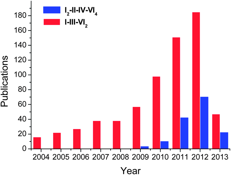 | ||
| Fig. 2 Number of publications regarding nanostructures of I–III–VI2 and I2–II–IV–VI4 compounds till April 2013. The results come from the Web of Science database. | ||
| Year | Compound | Cation and anion sources | Reaction solvents | Reaction temperature | Crystalline phases | Nanocrystal morphology | E g/eV | Ref. |
|---|---|---|---|---|---|---|---|---|
| 1999 | CISe | CuCl, InCl3 and TOPSe | TOPO | 250 °C | — | Quantum dots | 2.95 | 84 |
| 2004 | CIS | (PPh3)2CuIn(SEt)4 | Dioctyl phthalate, hexanethiol | 200 °C, 225 °C, 250 °C | Tetragonal | Irregular | — | 85 |
| 2006 | SIS | [(Ph3P)2Ag(m-SC{O}Ph-S)2In(SC{O}Ph)2] | DDT, OA | 200 °C | Orthorhombic | Irregular | — | 86 |
| 2006 | SISe | [(PPh3)2AgIn-(SeC{O}Ph)4] | OLA, DDT | 185 °C | Orthorhombic | Nanorods | — | 87 |
| 2006 | CIS | CuI, InI3 and S | TOP, ODE, OLA | 160–280 °C | Chalcopyrite | Irregular | 1.8 | 88 |
| 2008 | CIS | Cu(dedc)2 and In(dedc)3 | OLA, OA, DDT | 180 °C | WZ, ZB | Irregular | 1.45 | 89 |
| 2008 | CISe | CuCl, InCl3 and Se | OLA | 285 °C | Chalcopyrite, sphalerite | Irregular, nanorings | 1.06 | 90 |
| 2008 | CGSe | Cu(acac)2, Ga(acac)3 and Se | OLA | 250 °C | Tetragonal | Irregular | 1.7 | 91 |
| 2009 | CZTS | Cu(acac)2, Zn(acac)2, Sn(acac)2Br2 and S | OLA | 225 °C | Tetragonal | Irregular | 1.5 | 92 |
| 2009 | CZTS | Cu(acac)2, Zn(AcAc)2, SnCl2 and S | OLA | 280 °C | Tetragonal | Irregular | 1.3 | 24 |
| 2009 | CZTS | Cu(acac)2, Zn(CH3COO)2, Sn(CH3COO)4 and S | OLA, TOPO | 300 °C | Tetragonal | Irregular | 1.5 | 21 |
| 2009 | CIS | CuCl, InCl3 and thiourea | OLA | 240 °C | Polytypic | Nanodisks | 1.53 | 93 |
| 2009 | CISe | CuCl, InCl3 and selenourea | OLA | 240 °C | Tetragonal | Nano-pyramidals | 1 | 94 |
| 2010 | CIS | CuAc, InAc3, 1-DDT and t-DDT | TOPO, OLA | 240 °C | WZ | Elongated nanoparticles | 1.5 | 95 |
| 2010 | CISe | CuCl, In(acac)3, and diphenyl diselenide | OLA | 180 °C | WZ | Irregular | 1.19 | 96 |
| 2011 | CZTS | CuCl2·2H2O, ZnCl2, SnCl4·5H2O and DDT | DDT, OLA, OA | 240 °C | WZ | Nanoprisms, nanoplates | 1.4 | 97 |
| 2011 | CCTSe | Cu(acac)2, Sn(acac)2Cl2, Cd(CH3COO)2 2H2O and SeO2 | OLA, ODE | 300 °C | Stannite | Irregular | 1.1 | 33 |
| 2012 | CZTS | Cu(acac)2, Zn(CH3COO)2, Sn(CH3COO)4, 1-DDT and t-DDT | TOPO, ODE | 240–260 °C | WZ | Nanorods | 1.43 | 98 |
| 2012 | CZGeSe | CuCl, ZnO, GeCl4 and SeO2 | HDA, ODE | 295 °C | Tetragonal | Nano-tetrahedron | — | 34 |
| 2012 | CZTSSe | CuI, Zn(CH3COO)2·2H2O, SnCl2·2H2O, DDT and diphenyl diselenide | OLA | 280 °C | Polytypic | Rugby-ball-like | 1.1 | 48 |
Up to now, most of the important I–III–VI2 and I2–II–IV–VI4 nanocrystals have been prepared, such as CuInS2 (CIS), CISe, CuGaS2 (CGS), CuGaSe2 (CGSe), SIS, AgInSe2 (SISe), CZTS, CZTSe, CCTSe and Cu2ZnGeSe4 (CZGeSe) (Table 1, Fig. 3 and 4); novel metastable WZ-derived phases have been discovered; bandgap engineering in nanocrystals and shape controlled syntheses have been realized in some important compounds; the formation pathways of these complex compounds have been studied. Due to their similarity in crystalline and electronic structures, it is interesting to find there are some common features among the synthetic routes and formation processes of different I–III–VI2 and I2–II–IV–VI4 nanocrystals, which will be discussed in detail in the following content.
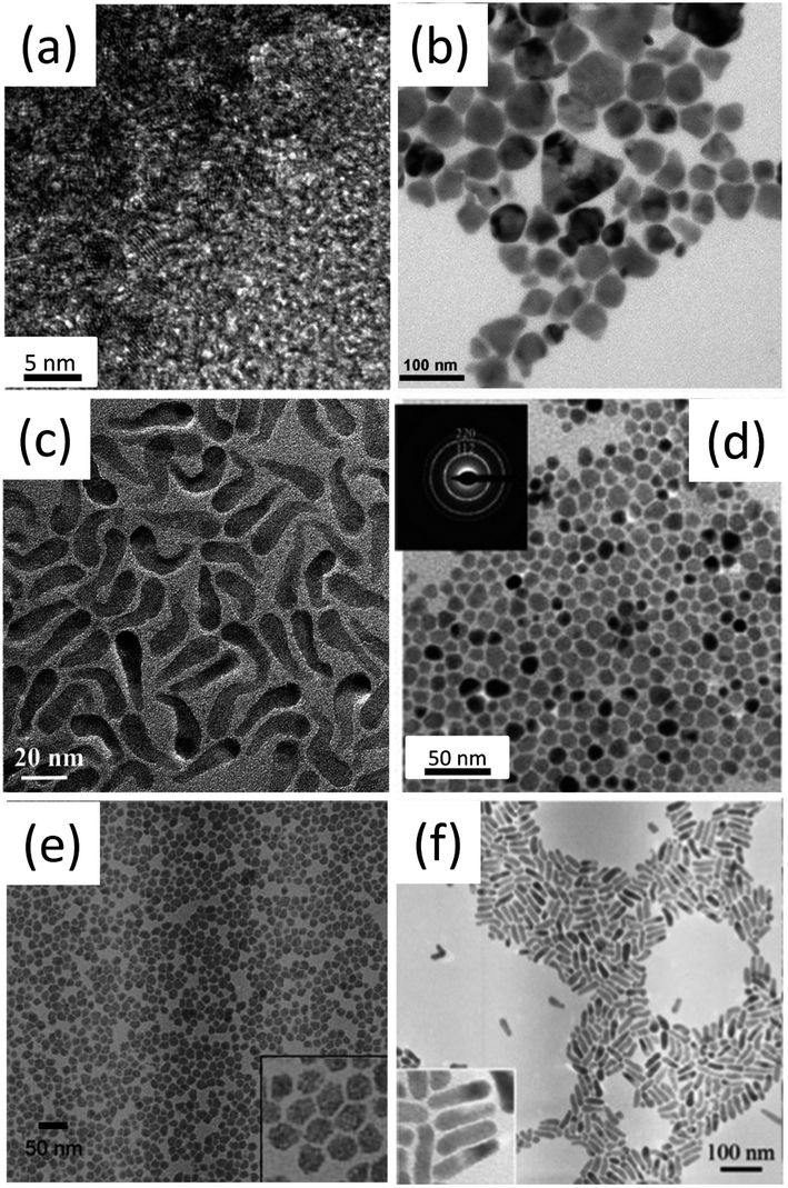 | ||
| Fig. 3 Bright-field transmission electronic microscopy (TEM) images of (a) CIS, (b) CISe, (c) CuGaS2 (CGS), (d) CGSe, (e) SIS and (f) SISe nanocrystals. Reproduced with permission from the American Chemical Society and The Royal Society of Chemistry from ref. 85–87, 90, 91 and 99. | ||
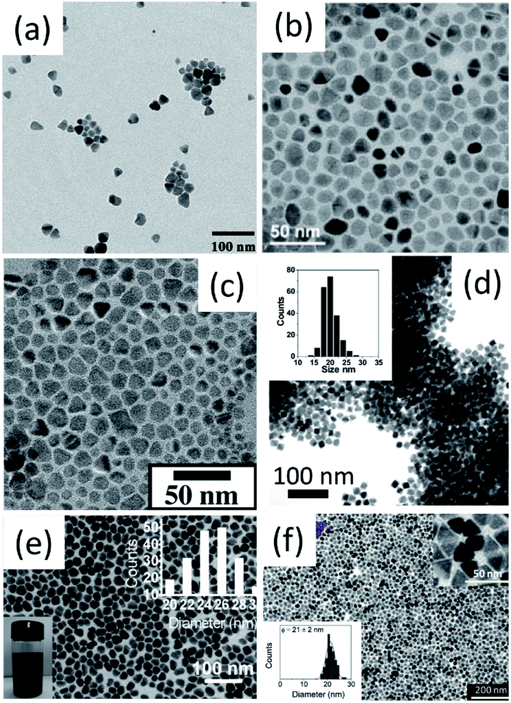 | ||
| Fig. 4 Bright-field TEM images of (a) CZTS, (b) CZTS, (c) CZTS, (d) CZTSe, (e) CCTSe and (f) CZGeSe nanocrystals. Reproduced with permission from the American Chemical Society from ref. 20–22, 24, 33 and 34. | ||
3.1 Phase-selective syntheses of I–III–VI2 and I2–II–IV–VI4 nanocrystals
Firstly, elemental S, thiourea, elemental Se and SeO2 are the most commonly used anion sources for synthesizing I–III–VI2 and I2–II–IV–VI4 nanocrystals, and the obtained nanocrystals all crystalize in thermodynamically stable ZB-derived phases (Table 1). It is easy to understand that the formation energies are the most important contribution to the total energies of the nanocrystals, so nanocrystals tend to crystalize in stable phases to lower their total energies. As we discussed in Section 2.1, although it is very hard to determine whether the precise structure of the synthesized I2–II–IV–VI4 nanocrystals is kesterite or stannite, it is clear that their anion matrices are similar to those of binary ZB chalcogenides. In addition, (I + II) atoms disorder has a low energy cost and thus they are very possible in cation matrices of I2–II–IV–VI4 nanocrystals.Secondly, I–III–VI2 and I2–II–IV–VI4 nanocrystals with metastable WZ-derived phases can be synthesized by using proper S (or Se) sources or forming proper cation-complexes to offer certain kinetic control during the growth process. Surfactant capping at the surface of metastable nanocrystals, which decreases the surface free-energy, might be another contribution to stabilize metastable phases. As we know, for nanostructures with high specific surface areas, the surface free energy contributes a lot to the total energy.
Pan et al. reported the first phase tunable synthesis of CIS nanocrystals, which is also the first case among I–III–VI2 compounds.89 When other reaction parameters are kept the same, exchange of surfactant from OA to DDT triggers the transformation of CIS nanocrystals from the ZB to the WZ phase. Brutchey et al. reported the first synthesis of WZ CISe nanocrystals,96 where diphenyl diselenide was used as the selenium source and it has been proven to play an key role in the formation of the metastable WZ CISe phase. The basic synthesis principles developed by Pan et al.89 and Brutchey et al.96 have been subsequently proven to be extendable to other ternary and quaternary chalcogenides. Brutchey et al., Peng et al. and Wan et al. prepared metastable WZ-derived Cu2SnSe3 (CTSe),100 CZTS97 and CZTSe101 nanocrystals by using di-tert-butyl diselenide, DDT and diphenyl diselenide as anion sources, respectively. Very recently, Yu et al. further demonstrated that DDT and diphenyl diselenide can be used together to obtain the alloys of WZ-derived CZTS and CZTSe.102
Thiol and diorgano diselenide have been found to play key roles to the growth of Cu-based WZ-derived multinary chalcogenides. These compounds are kinetic products beyond thermodynamic equilibrium; therefore, a fast nanocrystal growth is the precondition. As shown in Table 1, for the synthesis of ZB-derived CIS, CGS and CZTS, sulfur–OLA solutions were usually used as a sulfur precursor; they exist as alkylammonium polysulfides at low temperatures, and the polysulfide ions react with excess amine to generate H2S at elevated temperature,103 which combines with the metal precursors to form metal sulfide nanocrystals. DDT can form thiolate with metal salts upon heating,104,105 which will decompose directly to form metal sulfide nanocrystals, so a faster growth of nanocrystal can be obtained and the final nanoparticles crystalize in metastable WZ-derived phases. Furthermore, when thiol rather than sulfur powder was used as the sulfur source, the obtained products are usually nanorods or hexagonal discs,97–99 indicating that the DDT is an efficient capping agent to passivate the crystalline facets of the WZ-derived phase, and thus lower the total energies of the nanocrystals. For the syntheses of CISe and CZTSe, a dispersion of selenium powder in OLA has been used as the selenium source to synthesize ZB-derived nanocrystals;90,91,106 before combination of selenium with metal precursors, selenium powder dissolves upon heating and forms diorganodiselenide,107 and thus reaction slows down due to this step. TOPSe has also been used as selenium source for Cu-based multinary selenides, but this also shows lower reactivity than diorganodiselenide due to the strong bond between TOP, so the obtained nanocrystals are also crystallized in the thermodynamically stable phases.107 For diorganodiselenide, it reacts with cation sources directly and thus a fast growth occurs, leading to the formation of metastable phases.
Omata et al. also reported the phase selective synthesis of CIS nanocrystals.108 They prepared a metal–trioctylphosphine complex and S/trioctylphosphine solutions as cation and anion sources, respectively, 1-HDA and OLA were used as capping agents. These precursors and surfactants were mixed as the starting solutions, which were preserved for different times before the reactions were triggered. For a short preserve time of 3 min, the synthesized nanocrystals crystallize in a ZB-derived phase, and for a longer preserve time of 3 h, metal–TOP complexes react with OLA and form metal–OLA complexes due to stronger bonds between the metal ions and OLA, the obtained nanocrystals have a WZ-derived phase. A possible mechanism has been proposed for the selective growth of CIS nanocrystals with two different phases: when metal ions are coordinated with OLA, the consumption of the metal ions is very low during the nucleation stage, and thus a fast nanocrystal growth occurs, yielding nanocrystals with a metastable WZ phase, because a large amount of the metal ions remained after nucleation.
It should be noted that cation occupations in WZ-derived CZTS and CZTSe were taken as totally disordered. However, unlike the small formation energy gap between ZB- and WZ-derivatives, the high energy costs caused by total cation disorder makes the structures unstable.44,47,109 Zhan et al. reported the synthesis of WZ-derived CZTS through a hydrothermal process with the assistance of ethylenediamine; metal chloride and thiocarbamide were used as precursors, the split of some diffraction peaks in powder X-ray diffractions was proposed to be an indicator of the cation-ordered orthorhombic structure rather than the cation-disordered WZ structure.110
Thirdly, phase determination of I–III–VI2 and I2–II–IV–VI4 nanocrystals can also been affected by the reaction temperature. Vittal et al. reported the phase-selective synthesis of CIS nanocrystals by adjusting the reaction temperatures.111 With the TOPO![[thin space (1/6-em)]](https://www.rsc.org/images/entities/char_2009.gif) :DTT ratio kept as 1:1, they obtain WZ-derived CIS below 250 °C and ZB-derived CIS above 250 °C. Very recently, we reported the controlled synthesis of polytypic CZTSSe nanocrystals, and found the phase ratio of ZB- to WZ-derivatives increases with increasing the reaction temperature.48 These results are consistent with the idea that a thermodynamically stable phase can be obtained at relatively high reaction temperatures, which can be understood as follows: although the growth rate of nanocrystals is faster at higher temperatures, and thus will promote the crystallization of metastable phase, the lattice vibration or thermal activation is also stronger at high temperatures, so that it will be easier for cations and anions to combine at the sites of thermodynamic stable phase to lower the formation energy of the nanocrystals.
:DTT ratio kept as 1:1, they obtain WZ-derived CIS below 250 °C and ZB-derived CIS above 250 °C. Very recently, we reported the controlled synthesis of polytypic CZTSSe nanocrystals, and found the phase ratio of ZB- to WZ-derivatives increases with increasing the reaction temperature.48 These results are consistent with the idea that a thermodynamically stable phase can be obtained at relatively high reaction temperatures, which can be understood as follows: although the growth rate of nanocrystals is faster at higher temperatures, and thus will promote the crystallization of metastable phase, the lattice vibration or thermal activation is also stronger at high temperatures, so that it will be easier for cations and anions to combine at the sites of thermodynamic stable phase to lower the formation energy of the nanocrystals.
Actually, a deeper understanding of the formation mechanism of the metastable WZ-derived phases, e.g., why a fast growth of nanocrystals leads to the crystallization of the WZ-derived structure, is missing. This is probably because that these metastable phases have just been discovered for several years, and their advantages over the corresponding stable ZB-derived phases have not yet been proven. Recently, Wang et al. performed an ab initio calculation of WZ-type CISe,52 it is interesting to find that WZ-type CISe has an improved band structure for the absorption of visible and infrared light compared to the chalcopyrite CISe, indicating that WZ-type CISe might show superior photovoltaic performance to chalcopyrite CISe. Once this predication has been proven in real device performance, more efforts should be made in order to understand the formation mechanism of these WZ-derived phases, and thus more developed synthetic approaches should be employed to prepare WZ nanocrystals with low-cost and high yield.
Fourthly, thermodynamic ZB-derivatives and kinetically-stable phase WZ-derivatives can co-exist in single nanoparticles and form polytypic nanocrystals. Korgel et al. reported their novel discovery of polytypism in the CIS nanodiscs, where WZ phase interfaces with significant chalcopyrite domains.93 We recently reported the controlled synthesis of linearly arranged polytypic CZTSSe nanocrystals with a high yield.48 Each synthesized polytypic CZTSSe nanocrystal has a WZ-derived central domain and two ZB-derived ends, representing a rugby-ball-like morphology (Fig. 5). It has been found that although different polymorphs CZTS (or CZTSe) have the same chemical composition, they have slightly different electronic band structures.47 It has already been predicted that the type-II bandgap alignment exists on the WZ/ZB CdX (X = S, Se and Te) interface,112 and it also occurs on the interface of different GaInP2 polymorphs.43 For these reported polytypic CIS and CZTSSe nanocrystals, they would also benefit from the introduced type-II interface, which would lead to a better charge-carrier separation, and thus have potential photovoltaic applications.
 | ||
| Fig. 5 (a) A typical low magnification bright-field TEM image of the polytypic CZTSSe nanocrystals, (b and c), bright-field and dark-field TEM images of one single polytypic CZTSSe nanocrystal, (d) a typical HRETM image of single polytypic CZTSSe nanocrystals. Reproduced with permission of Nature Publishing Group from ref. 48. | ||
3.2 Bandgap tunable syntheses of I–III–VI2 and I2–II–IV–VI4 nanocrystals
Colloidal nanocrystals with a proper bandgap are the foundation of colloidal nanocrystal-based solar cells, and thus their syntheses are the initial steps towards high performance devices. As we discussed in Section 2.2, bandgaps of these I–III–VI2 and I2–II–IV–VI4 chalcogenides can be increased through adjusting the III–VI and IV–VI bond lengths via tuning S/Se and cation ratios. Actually, this principle has been realized experimentally in I–III–VI2 and I2–II–IV–VI4 nanocrystals. In the following, we will discuss this in detail.Firstly, bandgap tunable syntheses of I–III–VI2 and I2–II–IV–VI4 nanocrystals can be achieved through adjusting the S/Se ratio. For I2–II–IV–VI4 compounds, there are several reports on the synthesis and bandgap tuning of CZTSSe nanocrystals through adjusting the S/Se ratio. Zhang,113 Parkinson,114 Chang115 and co-workers reported three similar synthetic approaches to tetragonal CZTSSe nanocrystals, where the S/Se ratios were all adjusted by tuning the relative amounts of sulfur and selenium powder. However, there are some discrepancies among their results concerning the bandgaps of the resulting nanocrystals. Parkinson et al. reported that the bandgap of the CZTSSe nanocrystals can be continuously adjusted from 1.52 eV for pure CZTS to 1.47 eV for pure CZTSe (Fig. 6a),114 but Chang et al. showed that a much larger tunable range of 0.5 eV (from 1.5 to 1.0 eV) can be achieved.115 Chen et al. investigated theoretically some of the fundamental properties of kesterite CZTSSe as a function of alloy composition x through first-principles calculations,116 and they found the bandgaps of randomly mixed alloys increase from 1.0 eV to 1.5 eV with increase in S content, and the bowing parameter is small. The result is also consistent with the result recently reported by Khare et al.117 Assuming that the quantum confinement effect is not noticeable in these alloy nanocrystals, the result reported by Chang et al. is closer to that calculated by first-principles calculations as well as observed from thin film samples.116,118
 | ||
| Fig. 6 Estimated bandgaps of (a) ZB-derived CZTSSe nanocrystals, (b) WZ-derived CZTSSe nanocrystals, (c) ZB-derived CZGSS nanocrystals and (d) ZB-derived CZTS quantum dots. Reproduced with permission from the American Chemical Society and The Royal Society of Chemistry from ref. 102, 114, 121 and 122. | ||
Talapin and co-workers developed a novel route to CZTSe and CZTSSe films.119 Sn2Se62−-capped colloidal Cu2Se and ZnS nanocrystals were used as soluble precursors to fabricate CZTSSe films by depositing and annealing them at 500 °C in an inert atmosphere. When ZnS nanocrystals were substituted with ZnSe nanocrystals, the obtained films crystallize in the pure CZTSe phase and the chemical composition can be tuned. If Sn2Se62− was further substituted with Sn2S62−, CZTSSe with a different S/Se ratio can be obtained. The bandgap of the resulted CZTSSe films increases from 1.16 eV to 1.44 eV with S/Se increasing from 0.33 to 3.
Compared with ZB-derived CZTSSe alloys, WZ-derived CZTSSe alloys are more difficult to synthesize with two-fold energetic metastability, that is, WZ-derived CZTSSe are metastable relative to the ZB-derived alloys, and the alloys are metastable relative to the phase-pure compounds. We recently reported the composition and bandgap tunable synthesis of WZ-derived CZTSSe alloys, and a tunable bandgap range from about 1.0 to 1.5 eV was observed that shows good agreement with the ab initial calculations (Fig. 6b).102
Bandgap tunable synthesis of I–III–VI2 nanocrystals through adjusting the anions ratio has been less reported. Tuan et al. reported the synthesis of chalcopyrite CuIn(S1−xSex)2 (CISSe) nanocrystals through reacting CuCl, InCl3, S, and Se in OLA. The bandgap of the synthesized CISSe nanocrystals can be tuned nonlinearly from 0.98 to 1.46 eV, and a bowing parameter of 0.17 eV was observed.120
Secondly, bandgap tunable syntheses of I–III–VI2 and I2–II–IV–VI4 nanocrystals can also be achieved through adjusting the cation matrix. Sargent et al. reported a colloidal synthesis of a nanocrystal alloy of CISe and CGSe through tuning the relative amount of In and Ga sources; the synthesized Cu(InGa)Se2 nanocrystals were reported to have a bandgap value of 1.2 eV, which is larger than CGSe nanocrystals (1.03 eV) and smaller than CISe (1.7 eV) nanocrystals.91 Bao et al. reported the synthesis of Cu(In1−xGax)S2 nanocrystals; an almost linear tunable window from 1.53 eV to 2.48 eV was observed.99 Hillhouse and co-workers reported the synthesis of Cu2Zn(Ge1−xSnx)S4 (CZTGeS) nanocrystals modified from those of CZTS nanocrystals by replacing Sn(acac)2Cl2 with an equivalent molar amount of GeCl4, and they found that the bandgap of the CZTS nanocrystals can be increased from 1.5 to 1.93 eV by increasing the Ge content (Fig. 6c).123 Zhan et al. reported another approach to tuning the bandgap of non-stoichiometric CZTS nanocrystals. They prepared sphalerite-type (Cu2Sn)x/3Zn1−xS (0 ≤ x ≤ 0.75) nanocrystals, with tunable bandgaps ranging from 3.48 eV to 1.23 eV depending on the composition parameter x.124
Thirdly, bandgap tunable syntheses of I–III–VI2 and I2–II–IV–VI4 nanocrystals can also be realized through scaling-down the particle size. The quantum confinement effect has be applied to engineer efficiently the bandgaps of binary chalcogenide nanocrystals when the sizes of nanocrystals are smaller than their exciton Bohr radius.125,126 For I–III–VI2 quantum dots, Omata et al. performed a systematic theoretical study on the size-dependent optical band gap, where they confirmed that the optical band gaps of I–III–VI2 quantum dots can cover a wide wavelength range from the ultraviolet to near-infrared.127 Bawendi reported the syntheses of Cu–In–Se nanocrystals with variable compositions and sizes; they experimentally observed red to near-infrared photoluminescence of nanocrystals which depend on both size and composition.128 Teng et al.129 and Scholes et al.130 reported size-tunable syntheses of CIS quantum dots via adjusting the reaction temperature and time, respectively. Size-dependent bandgaps have also been experimentally observed.
I2–II–IV–VI4 nanocrystals with sizes down to several nanometers have been even less reported. Synthesis of near stoichiometric quaternary nanocrystals usually needs a long reaction time, usually longer than 0.5 h, otherwise, the cation ratios can be hardly controlled, but a long reaction time usually yields large nanocrystals. So, it is hard to get very small I2–II–IV–VI4 nanocrystals with a stoichiometric composition. Norris et al. reported an interesting approach to CZTS quantum dots through the addition of OLA to lower the decomposition temperature of all copper, zinc, and tin diethyl dithiocarbamate complexes, and thus, simultaneous decomposition of these complexes can be triggered to a narrow temperature range to obtain the nucleation and subsequent growth of CZTS nanocrystals with small sizes.122 By varying the amount of OLA injected and the growth temperature, the average diameter of the nanocrystals can be tuned, and the growth time of the nanocrystals was found not to affect the final nanocrystal size. It has been demonstrated that the bandgap of CZTS quantum dots can be tuned from 1.5 eV to 1.8 eV (Fig. 6d).122
Very recently, we reported our finding that the phase ratio of ZB to WZ has a certain effect on th bandgap of polytypic CZTSSe nanocrystals.48 Actually, previous research has also revealed that the band-gaps of GaAs nanowires could be adjusted from 1.515 eV to 1.43 eV by introducing an increasing proportion of the WZ phase into ZB nanowires; the redshift in bandgap can be understood by the carrier confinement which is induced by the band-offset staging between ZB and WZ segments, and this mechanism could also be applied to explain what we have found in CZTSSe polytypic nanocrystals.131
3.3 Shape controlled syntheses of I–III–VI2 and I2–II–IV–VI4 nanocrystals
The deposition and consolidation of I–III–VI2 and I2–II–IV–VI4 nanocrystals into thin films or bulk materials are necessary steps for the realisation of their photovoltaic and thermoelectric applications. The deposition of mono-dispersed as well as morphology controlled nanocrystals can result in high density packing, which will lead to high charge mobility and is a positive condition for high-performance devices. However, the synthesis of I–III–VI2 and I2–II–IV–VI4 nanocrystals with well-controlled morphologies still remains a challenge; most of the reported nanocrystals are usually irregular in shape and slight polydispersed in size (Table 1, Fig. 3 and 4). It is interesting to note that when the synthesized nanocrystals crystalize in WZ-derived phases, nanorods and hexagonal nanoplates with the axial direction along the c axis can be obtained easily. For example, WZ-derived SISe,87 CIS,132 CIGS99 and CZTS (Fig. 7c and d) nanorods98 have been prepared, furthermore, WZ-derived CIS93 and CISe133 hexagonal nanoplates have also been obtained. For ZB-derived nanocrystals, morphology-controlled syntheses have been much less reported; pyramidal CIS130 and CISe94 nanocrystals were reported by Scholes et al. and Korgel et al. (Fig. 7a and b), respectively. Cabot et al. recently reported the morphology controlled synthesis of CCTSe with tetrahedral and penta-tetrahedral shapes.134 The formation of metal–alkylphosphonic acids was proposed to play key role to obtain stoichiometric nanocrystals, and alkylamines were proven to be an efficient capping agents, which control the size and shape of nanocrystals.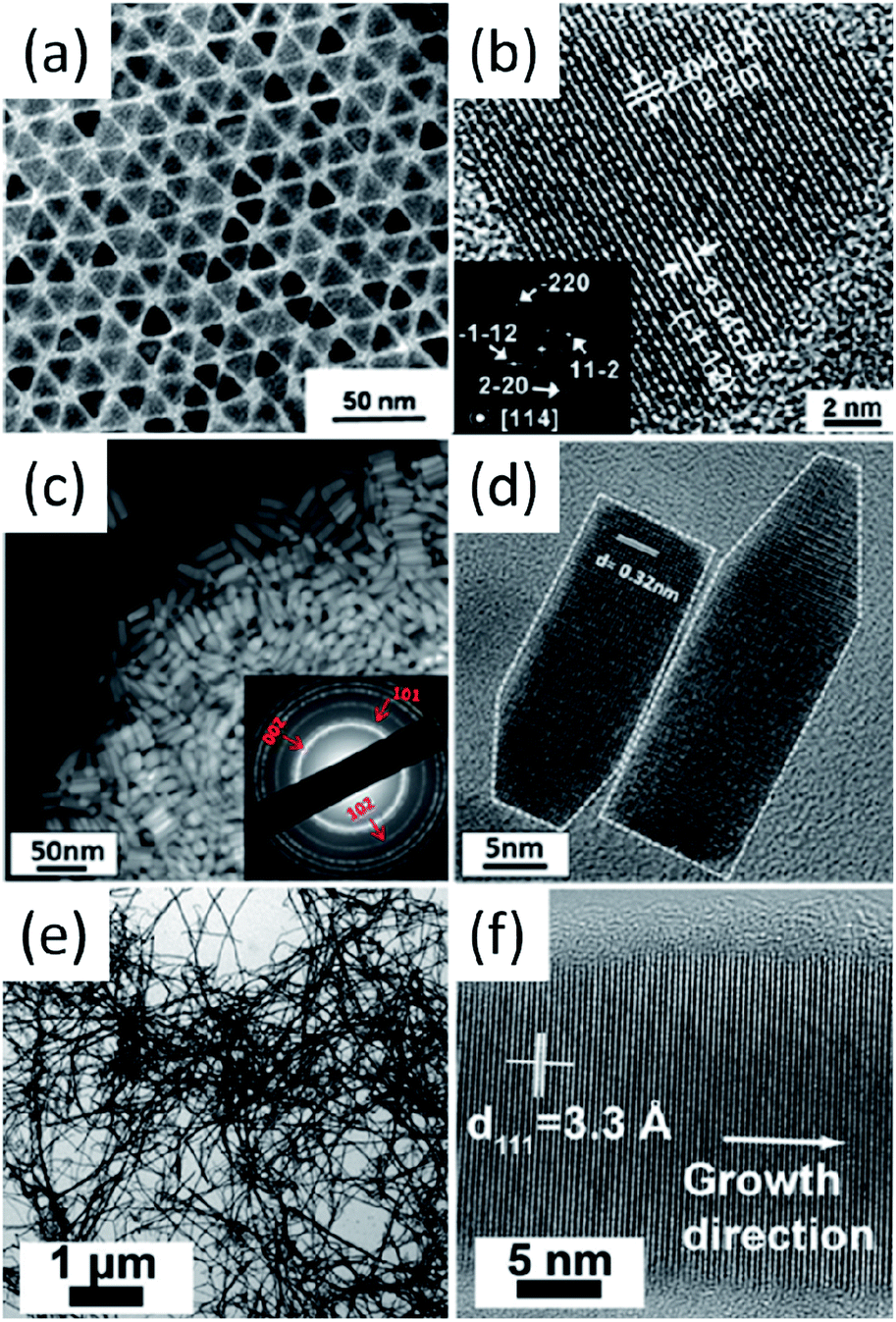 | ||
| Fig. 7 (a and b) bright-field TEM and HRTEM images of pyramidal CISe nanocrystals; (c and d) dark-field TEM and HRTEM images of WZ-derived CZTS nanorods; (e and f) bright-field TEM and HRTEM images of tetragonal CISe nanowires. Reproduced with permission from the American Chemical Society from ref. 94, 98 and 135. | ||
Nanowires bring new possibilities to improve minority carrier diffusion lengths and thus higher efficiencies can be expected in nanowires incorporated solar cells.136 To test and verify this hypothesis, solid–liquid–solid (SLS) growth of CISe nanowires has been developed by several groups (Fig. 7e and f),135,137,138 Korgel et al. further demonstrated that the nanowires can be compacted into paper-like films, they also fabricated solar cell devices by using the nanowires as active absorbance layers,135 but the power conversion efficiency was too low due to the low shunt resistance. WZ CIS nanowires have also been prepared by using Ag2S nanoparticles as catalysts.139 Furthermore, template-mediated method has been applied to synthesise ternary and quaternary chalcogenide with designed one-dimensional morphology. Both sacrificial and hard templates were applied to synthesize CISe, CZTS and CZTSe nanowires.140,141
3.4 Up-scaled approaches to CZTS and CZTSe nanocrystals
As we have discussed above, colloidal syntheses of I–III–VI2 and I2–II–IV–VI4 nanocrystals are usually based on the decomposition and reaction of precursors in high boiling organic solvents, such as OLA, ODE and TOP (Table 1). A typical reaction yields about several tens or hundreds of milligrams of products. Given the promising future of a solar cell produced from “nanocrystals ink”, the scalability of nanocrystal syntheses needs to be considered. Actually, the scalability of production is rather important for research and application of thermoelectric nanocrystals, because the compaction of solid discs (or cylinders), which is usually necessary for thermoelectric property characterization, requires a gram of powder.Scholes et al. and Tuan et al. reported the non-injection synthesis of CIS and CISSe nanocrystals yielding over a gram of product.120,130 For larger production, we recently reported a scale-up synthesis of non-stoichiometric CZTSe nanocrystals by using OLA and ODE as reaction media (Fig. 8). Precursors at high concentration were involved in the reactions and large reaction flasks were used for to obtain over 10 grams of product per run. Notably, SeO2 was chosen as the selenium source rather than selenium powder. SeO2 shows advantages in large scale synthesis, because it is easier to dissolved than selenium in ODE and not sensitive to oxygen. Cabot et al. reported a successful and continuous production method to obtain relatively large amounts of quaternary chalcogenide nanoparticles, in particular CZTS, with controlled chemical composition.143 The procedure was used for preparing grams of this material with controlled composition under atmospheric environmental conditions. There is another similar work presented by Grover et al., where a supercritical carbon dioxide continuous-flow reactor is applied to deposit CZTS micro- and nanoparticles onto a silicon wafer from metal dithiocarbamate precursors.144
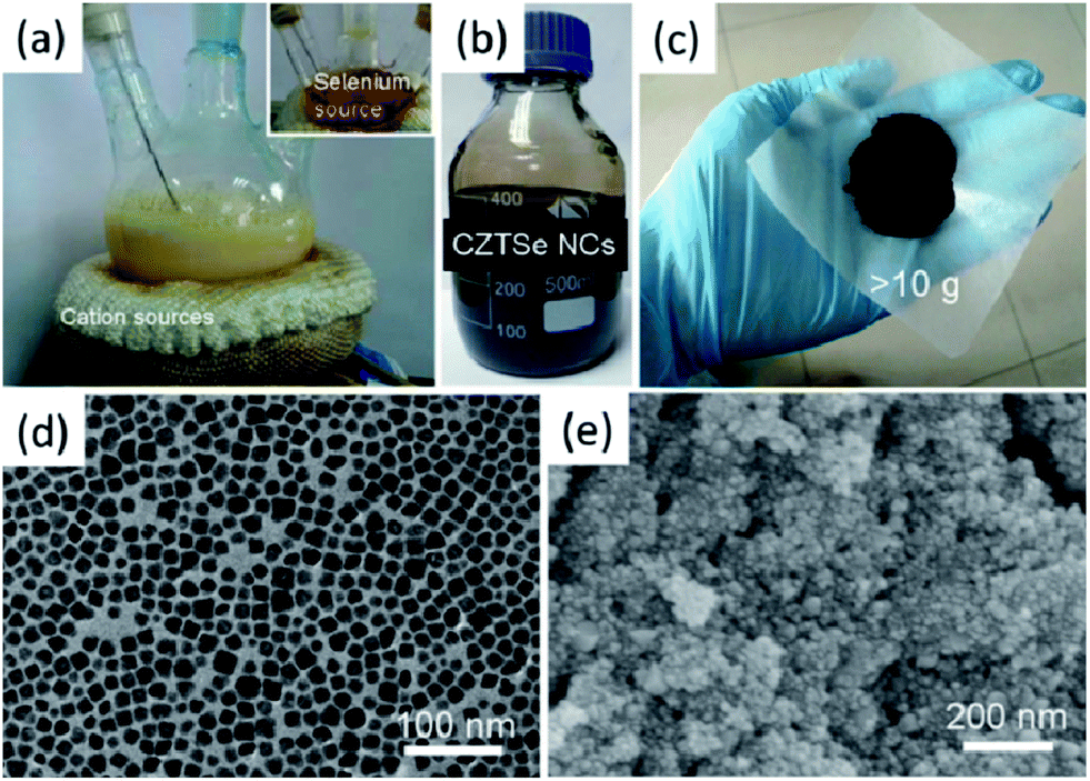 | ||
| Fig. 8 Photographs of the reaction flasks (a), synthesized non-stoichiometric CZTSe nanocrystals/hexane dispersion (b) and powder of surface-clean non-stoichiometric CZTSe nanoparticles (c). TEM (d) and SEM (e) images of the non-stoichiometric CZTSe nanoparticles Reproduced with permission of Wiley-VCH Verlag GmbH & Co. KGaA from ref. 142. | ||
3.5 Formation pathways of these multinary chalcogenides
While more attention has been paid to the properties of these ternary and quaternary chalcogenides, and expanding the synthetic procedures to cover more I–III–VI2 and I2–II–IV–VI4 nanocrystals is an important topic of present researches, less attention has been paid to the growth pathways of these nanocrystals. Actually, why homogeneous ternary and quaternary chalcogenides rather than phase separated binary or ternary chalcogenides form might be a source of great speculation. This is because, according to the precipitation and dissolution equilibrium theory, different cations will deposit with anions sequentially according to the difference of solubility product (Ksp).Pan et al. proposed a formation pathway for the growth of CIS nanocrystals in which Cu2S and In2S3 (or InS) form at the initial stage and dissolve subsequently to form homogeneous CIS.89 Kuzuya et al. recently proposed that the CIS nanocrystals originate from the pre-generation of Cu2S seed nanoparticles and following cation exchange process, they pointed out that the phase of the CIS nanocrystals is determined by the phase of the Cu2S seeds.145 Agrawal et al. performed a careful study on the formation pathway of CISe nanocrystals; aliquots of the reaction intermediates were extracted at various temperatures during the reaction ramping process, the solid products were determined by powder X-ray diffraction and EDX analysis.146 They found that hexagonal γ-CuSe was formed firstly, then cubic InSe appeared at elevated reaction temperatures, finally, and ZB CISe was generated while γ-CuSe and InSe disappeared. Based on these observations, a formation pathway was proposed which can be described as CuSe + InSe → CISe.
For quaternary chalcogenide nanocrystals, Han et al. proposed a formation mechanism for WZ-derived CZTS nanocrystals based on the characterization of intermediate products.147 Cu1.95S nanocrystals were proposed to form at the nucleation stage, after anisotropic growth of WZ-derived CZTS onto one side of the Cu1.95S nanocrystals; cation exchange between the two parts eventually leads to phase-pure WZ-derived CZTS nanocrystals. They also proposed that the WZ-derived phase of CZTS nanocrystals is inherited from the hexagonal Cu1.95S nanocrystals. Cabot et al. found that the reactivities of Cu, Zn and Sn sources are in the order of Cu > Sn > Zn during their synthesis of CZTS nanocrystals, and thus they proposed a similar formation pathway of tetragonal CZTS nanocrystals that Sn and Zn atoms subsequently enter the nucleated Cu2S nanocrystals through cation exchange.143
We can find some common features of the proposed growth process of ternary and quaternary chalcogenide nanocrystals. Binary Cu-based chalcogenide nanocrystals were found firstly to nucleate due to the high reactivities between Cu-precursors and sulfur (selenium) sources, subsequent cation exchange occurs between the nucleated Cu-based binary nanocrystals and reaction solution. It is even possible for some binary chalcogenide nanocrystals to grow at the initial stage, e.g. InS and InSe; they will be dissolved again and enter Cu-based binary chalcogenide nanocrystals to form homogenous multinary compounds to lower the total energy.
3.6 Homogeneity of element distributions in these multi-nary chalcogenide nanocrystals
For the above-mentioned multinary chalcogenide nanocrystals, they are synthesized in solution, and thus the reaction temperatures are limited to be no higher than the boiling points of the solvents, usually equivalent to or below 350 °C; the question arises as to whether binary or ternary phases will coexist with the target products and whether there are composition variations among different particles. I–III–VI2 compounds can be easily distinguished from I–VI and III–VI compounds through PXRD analysis, but Cu2ZnSn(S/Se)4 can hardly be distinguished from ZnS/Se and Cu2Sn(S/Se)3 through the only PXRD analysis. To clarify this issue, Parkinson et al. performed differential thermal analysis of the nanocrystals21 and Korgel et al. conducted scanning transmission electron microscopy (STEM)-energy dispersive spectrum (EDS) elemental mapping to confirm the crystalline structure.24 Actually, Raman spectrum analysis is also a kind of simple but efficient method to distinguish CZTS from other binary and ternary sulfides, which has been widely applied in quaternary chalcogenide determination in thin film samples.148,149These qualitative analyses confirm the synthesized nanocrystals are quaternary chalcogenides but it is hard to detect whether there is composition variation among different nanocrystals. Haas et al. reported an interesting investigation on the composition of individual CZTSe nanocrystals with the help of the excellent spatial resolution of energy dispersive X-ray spectroscopy (EDX) and electron energy loss spectra (EELS) in the nanometer scale. It was found that even the average chemical composition of the obtained nanocrystals is stoichiometric, individual nanoparticles vary from each other in content of Cu, Zn and Sn.150 A similar phenomenon was subsequently observed when Cabot and co-workers were characterizing the chemical compositions of single CZTS nanoparticles; they found variations in chemical composition were even larger in those nanoparticles synthesized at lower temperatures.143 These results indicate that there are high densities of defects in the synthesized CZTS and CZTSe nanocrystals and further developments in composition controlled syntheses of these nanocrystals are called for.
4 Photovoltaic and thermoelectric applications of I–III–VI2 and I2–II–IV–VI4 nanocrystals
Upon now, the increasing reports on the colloidal syntheses of ternary and quaternary nanocrystals have been motivated mainly by the concept that the nanocrystal dispersions can be used as a “nanocrystal ink” to prepare the absorbance layers of thin film solar cells. The applications of these nanocrystals in bulk thermoelectric conversion have also drawn certain attention. In the following sections, we will summarize the applications of I2–II–VI2 and I2–II–IV–VI4 nanocrystals in photovoltaic and thermoelectric applications.4.1 Applications as “nanocrystal ink” in thin film solar cells
Alivisatos and co-workers firstly reported the fabrication of a solar cells absorber layer from a nanocrystals dispersion in 2002.11 Colloidal CdSe nanorods were co-dissolved with P3HT in a mixture of pyridine and chloroform to fabricate the absorbance layers; the final devices show an AM 1.5 solar power conversion efficiency (PCE) as high as 2.8%,151 but inorganic nanocrystals were only expected to improve the charge transport efficiency of conjugated polymers. Nozik et al. speculatively showed the device model based on all-inorganic quantum dot arrays,6 and in 2005, Alivisatos et al. reported the first all-inorganic nanocrystal solar cells with the structure of (Ca)Al/CdSe/CdTe/ITO.10 The fabricated device shows a PCE of 1.7% under standard one sun illumination.152In 2008, two groups reported independently CISe nanocrystal thin film solar cells with the same structure of Mo/CISe/CdS/ZnO/ITO (Table 2).90,153 The basic concepts of these two works are also the same: to prepare CISe absorbance layers through printing a “nanocrystal ink” rather than depositing them by a vacuum-based multistage co-evaporation process, and thus lower fabricating costs can be expected. The devices were fabricated through drop-casting the nanocrystal dispersion on Mo-coated soda lime glass, following chemical bath deposition of the CdS layer, and RF sputtering of the intrinsic ZnO and ITO layers. Agrawal et al. annealed the nanocrystal films under Ar flow, and then under Se vapor before chemical bath deposition of CdS. They were surprised to see the nanocrystals sintered to form large crystal grains on the length scale of the thickness of the film and the fabricated device exhibited an efficiency of 3.2% under AM1.5 illumination. Korgel et al. didn't anneal the absorbance layers at high temperature. The open circuit voltages (Voc) of the two reported devices are similar to each other, but the short cut current density (Jsc) of Agrawal et al.'s device is much larger than that of Korgel et al.'s; the lower efficiency of the latter device is mainly attributed to the high series and low shunt resistances. Korgel's group subsequently reported optimized devices with an absorbance layer thickness of around 150 nm processed from the CISe nanocrystal inks, under ambient conditions and without post-deposition high temperature treatment; they show power conversion efficiencies up to 3.1% (ref. 154) (Table 2). They found the device efficiency is mainly limited by charge carrier trapping in the nanocrystal layer. Agrawal et al. also reported the optimized devices. Void space in the sintered CISe nanocrystal films can be eliminated by utilizing substitution reactions that yield a controlled volume expansion of the film. They deposited the Cu(In1−xGax)S2 (CIGS) nanocrystal films and then exposed them to selenium to substitute most of the sulfur, yielding volume expansion and dense Cu(In1−xGax)(S1−ySey)2 (CIGSSe) absorber layers. Through this approach, a higher conversion efficiency of 4.76% under standard AM1.5 illumination was obtained (Table 2).155 Very recently, another exciting result comes from the same group. A total area power conversion efficiency as high as 12.0% under AM1.5 illumination has been achieved in the optimized CIGSSe solar cell. During their fabrication, alkanethiol was used as the solvent to disperse CIGS nanocrystals, resulting nanocrystal film over a larger area after knife-coating. In addition, CIGSSe film was soaked in NaCl aqueous film to obtain Na inclusion before selenization, a significant improvement in the size and packing of the CIGSSe grains can be obtained (Table 2).16
| Nanocrystal ink | Solar cell structure | V oc/mV | J sc/mA cm−2 | FF | PCE | Ref. |
|---|---|---|---|---|---|---|
| CISe NPs | Mo/CISe/CdS/ZnO/ITO | 302 | 3.2 | 25% | 0.24% | 153 |
| CISe NPs | Mo/CISe/CdS/ZnO/ITO | 280 | 25.8 | 39% | 2.82% | 90 |
| CISe NPs | Au/CuISe/CdS/ZnO/ITO | 410 | 16.3 | 46% | 3.1% | 154 |
| CIGS NPs | Mo/CIGSSe/CdS/ZnO/ITO | 393 | 29.7 | 44% | 5.14% | 155 |
| Multiphase CISe NPs | Mo/CISe/CdS/ZnO/Al–ZnO | 440 | 33.7 | 55% | 8.2% | 160 |
| CIGS NPs | Mo/CIGSSe/CdS/ZnO/ITO | 630 | 28.8 | 65.7% | 12.0% | 16 |
| CZTS NPs | Au/CdS/ZnO/CZTS/ITO | 321 | 1.95 | 37% | 0.23% | 24 |
| CZTS NPs | Silver paint/CdS/ZnO/CZTSe/ITO | 210 | 11.5 | 33% | 0.74% | 92 |
| CZTS NPs | (Ni/Al)/ITO/CdS/ZnO/CZTSSe/Mo | 430 | 31.2 | 53.9% | 7.23% | 23 |
| CZTGeS | (Ni/Al)/ITO/CdS/ZnO/CZTGeSSe/Mo | 640 | 21.5 | 49% | 6.8% | 123 |
| CZTS NPs | (Ni/Al)/ITO/ZnO/ZnS/CZTS/Mo/Al | 484 | 8.91 | 45.1% | 1.94% | 157 |
| CZTS NPs | DSSSC With a CZTSSe/FTO counter electrode | 800 | 17.7 | 52.2% | 7.37% | 158 |
| CZTS hierarchical microspheres | QDSSC with a CZTS/FTO counter electrode | 822 | 11.06 | 41% | 3.73% | 159 |
| CZTGeS | ITO/ZnO/CdS/CZTGeSSe/Mo | 464 | 29.2 | 62% | 8.4% | 25 |
| Binary and ternary chalcogenide NPs | ZnO/ITO/ZnO/CdS/CZTSSe/Mo | 451 | 29.0 | 64.9% | 8.5% | 156 |
CZTS and CZTSe have been considered as ideal candidates for CIGS based solar cells, because they consist of earth-abundant elements. Both of the two above-mentioned leading groups further reported CZTS (CZTSSe) solar cells proceeding from CZTS nanocrystals.24,92 Their device configurations and fabrication processes are similar to the CISe nanocrystal solar cells, however, the conversion efficiencies are all below 1% (Table 2). In the following work reported by Agrawal et al., they presented the exciting optimized CZTSSe solar cells, the best performing CZTSSe solar cell shows a total area efficiency of 6.7%, with an open circuit voltage of 0.42 V, short cut current density of 30.4 mA cm−2 and fill factor (FF) of 52.7%.23 They attributed the significant enhancement in the power conversion efficiency to the proper composition of the original CZTS nanocrystals and the development in the thin film coating method. It was interesting to find that the conversion efficiency further improves to 7.2% after being soaked for 15 min under one sun illumination, even the improvement is temporary (Table 2). Subsequently, the same group reported their exploration of higher power conversion efficiency through alloying CZTS with Cu2ZnGeS4 (CZGeS); the bandgap of the absorbance layer can be tuned by adjusting the Sn/Ge ratio. The highest efficiency of 6.8% was observed in the device with a Ge/(Ge + Sn) ratio of 0.7; the reported efficiency is lower than the previously reported CZTSSe device123 but they have recently reported an optimized device showing an enhanced efficiency of 8.4% (Voc = 0.464 V, Jsc = 29.2 mA cm−2, FF = 62%) (Fig. 9 and Table 2).25 Compared with their previously reported high performance CZTSSe devices, both the Voc and FF have been significantly improved even when a small sacrifice in Jsc was also observed. In their experiment, the prepared Cu2ZnSn1−xGex(S1−ySey)4 CZTGeSSe thin films after selenization represent an interesting bi-layer structure; nanocrystals in the top layers are well sintered but those at the bottom layers representing particulate-like morphology are still un-sintered. So it can be expected that a higher PCE could be obtained if an optimization in the annealing process can be obtained. Very recently, Cao et al. fabricated CZTSSe-based solar cell devices, of which the absorber layers were prepared by selenizing a mixture of binary and ternary chalcogenide nanocrystal ink rather than a pure CZTS nanocrystal ink; a high PCE of 8.5% (with Voc = 0.451 V, Jsc = 29.0 mA cm−2, FF = 64.9%)156 was observed for the device in which copper tin sulfide and ZnS and SnS nanocrystals were applied. Interestingly, they also found a similar bi-layer structure consists of a well and a poorly sintered layer.
 | ||
| Fig. 9 Cross section FE-SEM images of the (a) as-coated and (b) selenized CZGeS nanocrystals film on Mo coated glass. (c) I–V characteristics of the CZGSSe solar cell measured under AM 1.5 illumination. Reproduced with permissions of Elsevier B.V. from ref. 25. | ||
All of the above CZTS or CZTSSe thin film solar cells are processed from OLA-capped CZTS nanocrystals, which can be only dispersed in non-polar solvents, such as hexane and toluene. As we know, these non-polar organic solvents such as toluene and hexane have detrimental effects on the environment; this issue can be resolved through using hydrophilic nanocrystals as ink. Hu and his co-workers recently reported CZTS solar cells made from PVP-capped CZTS nanocrystals; they developed a roll-to-roll printing technique to prepare an absorbance layer from a CZTS/ethanol dispersion on a flexible Mo coated Al foil substrate.157 The nanocrystal films were annealed in the presence of elemental sulfur before the chemical bath deposition of the ZnS buffer layer, direct current magnetron sputtering of intrinsic ZnO, ITO and Ni/Al. The fabricated device shows a Voc of 0.484 V, Jsc of 8.91 mA cm−2, and an FF of 0.451 with a power conversion efficiency of 1.94%. Although the power conversion efficiency is much lower than that of the device reported by Agrawal et al., the fabrication process is more environmentally friendly.
Recently, Lin and his co-workers reported a dye-sensitized solar cell (DSSC) with CZTSSe counter electrodes through a similar approach to that reported by Agrawal et al.158 The three key components of a DSSC are a dye-sensitized semiconductor photoanode, an electrolyte with a redox couple and a counter electrode. The most commonly used counter electrode is fluorine-doped tin oxide (FTO) glass coated with a thin platinum layer. Substitution of platinum thin layers with low-cost semiconductors while maintaining high efficiency will depress the manufacturing cost. Lin et al. prepared CZTSSe thin films on FTO following a similar approach to that reported by Agrawal et al. and fabricated DSSCs using CZTSSe thin films as counter electrodes. The CZTSSe thin films are highly comparable with the Pt thin films when they are used in DSSCs with similar device configuration. A high power conversion efficiency of 7.37% was observed in the fabricated device. More recently, CZTS hierarchical microspheres have been used as an effective counter electrode material for quantum dot sensitized solar cells (QDSSC). QDSSC have similar structures to DSSCs, mainly differing in the QDSC photoanode. To make a comparison between CZTS and Pt photoanodes, they fabricated the QDSSC devices with two photoanodes; it was found CZTS photoanodes outperform Pt photoanodes.159
4.2 Applications in thermoelectric devices
Thermoelectric (TE) materials, which show promising applications in refrigeration and waste-heat-to-electricity conversion, have drawn considerable attention. The TE performance is quantified by the TE figure of merit ZT (ZT = σS2T/κ), where σ, S, T and κ are electric conductivity, Seebeck coefficient, absolute temperature and thermal conductivity, respectively. It is widely accepted that good thermoelectric materials are usually narrow bandgap semiconductors. Recently, Chen et al. reported Cu-26 and In-doped27 CZTSe presenting a fairly good thermoelectric performance, even though CZTSe is a wide bandgap semiconductor with low charge carrier mobility. They also found CCTSe, an analogue of CZTSe presenting reasonable ZT values after Cu-doping.28For these wide quaternary chalcogenides, diverse types of bonding inside the compound cause them to have naturally distorted structures that can scatter phonons efficiently, resulting in low thermal conductivities. Synthesis of these quaternary chalcogenide nanocrystals through a “bottom up” approach and subsequent consolidation into nanostructured bulk materials could introduce grain boundaries to further reduce the lattice thermal conductivity. We reported the first exploration of the thermoelectric properties of CCTSe nanostructured bulk materials compacted from wet chemistry synthesized nanocrystals. The transport properties of prepared nanostructured bulk materials have been investigated in two directions, i.e., parallel and perpendicular to the press directions. We found that the transport properties of the final bulk materials are highly isotropic. Compared with reported optimal bulk materials, the peak power factor of our nanostructured bulk materials is about 40% higher, which could be understood by the increment in electric conductivities. This is very interesting because most of the nanostructured bulk materials benefit from depressed thermal conductivities rather than an enhanced power factor. This also indicates that the power factor of the CCTSe can be further improved through further composition modulation. However, we did not observe noticeable depression in thermal conductivities, revealing that the induced crystalline boundaries played a limited role in scattering the phonons. The reported ZT value of 0.65 is equivalent to the reported optimized CCTSe bulk materials (Table 3).28 Subsequently, Cabot et al. also reported the thermoelectric performance of CCTSe nanostructured bulk materials compacted from wet chemistry synthesized nanocrystals; depressed thermal conductivities together with deteriorated electric conductivities were observed in the prepared dense pellets with lower densities, resulting a similar peak ZT value of 0.71 (Table 3).161
Chen et al. tested the thermoelectric properties of CZTS polycrystalline bulk materials, which show a ZT value of 0.39 after optimization through Cu-doping.28 To explore whether nanostructured CZTS bulk materials would benefit from the depressed thermal conductivities, Wu et al. reported thermoelectric properties of solid discs fabricated from the colloidal CZTS nanocrystals through spark plasma sintering (SPS) (Table 3). As expected, the dense materials showed lower thermal conductivities and electric conductivities, and thus no enhancements in the final ZT values were observed. Recently, Cabot et al. reported the thermoelectric properties of the hot-pressed CZGSe nanocrystals, a reasonable ZT value of 0.55 was observed in the optimized sample (Table 3).34 More recently, we reported the thermoelectric properties of non-stoichiometric CZTSe dense materials hot-pressed from the synthesized colloidal nanocrystals;142 it was found that the hot-pressing temperature had little influence on the final ZT values. The peak ZT of the prepared dense materials reaches 0.44 at 450 °C, a similar value to the-state-of-the-art values of CZTSe- and CuSnSe3-based compounds (Table 3).26,27,162
5 Conclusions and outlook
Due to the promising future in thin film solar cells and thermoelectric devices, I–III–VI2 and I2–II–IV–VI4 compounds, especially CIS, CISe, CIGSe, CZTS and CZTSe, have drawn much attention. The developed synthetic approaches to colloidal nanocrystals at relative low temperatures provide new opportunities to fabricate low-cost and high performance devices. Recent reports have covered the syntheses of most of the important I–III–VI2 and I2–II–IV–VI4 nanocrystals (Table 1); the already extracted common features in syntheses and achieved theoretical understandings will serve as guidelines to synthesize other unreported analogous nanocrystals with designed phases and bandgaps. However, there are still some problems existing in recent researches.Firstly, a deeper understanding of these nanocrystals is still recommended. For example, in most reports, researchers ascribed the structure of ZB-derived CZTS nanocrystals to the cation-ordered tetragonal phase,21,24,92 but they ascribed the WZ-derived CZTS as totally cation-disordered WZ structure.92 Actually, as has been found both experimentally46 and theoretically,109 (Cu + Zn) disorder is highly possible due to the low energy cost while the (Cu + Sn) disorder is energetically unstable, thus both proposed crystal structures of CZTS nanocrystals might be inaccurate to some extent. Furthermore, bandgap determination of some quaternary I2–II–IV–VI4 nanocrystals is still confusing; as the bandgaps of the thin film kesterite CZTS and CZTSe make clear, i.e., about 1.5 and 1.0 eV, respectively.32,109,163 However, there are still some debates on the bandgaps of the CZTSe nanocrystal samples, for which the bandgap seems to be overestimated, e.g., the bandgap of the ZB-derived CZTSe has been reported to be 1.47 eV114 (Table 4).
| Compound | Crystal structure | Bandgap/eV |
|---|---|---|
| CZTS | ZB-derivative | 1.3 (ref. 24), 1.5 (ref. 21 and 92), 1.5 (ref. 164) |
| CZTSe | ZB-derivative | 1.4–1.5 (ref. 20), 1.3 (ref. 164), 1.52 (ref. 106) |
| CZTSSe | ZB-derivative | 1.47–1.54 (ref. 114), 1.28–1.50 (ref. 113) |
| CZTS | WZ-derivative | 1.4 (ref. 97), 1.43 (ref. 98) |
| CZTSe | WZ-derivative | 1.46 (ref. 101) |
Secondly, the fabricating costs of those photovoltaic devices processed from nanocrystals are still relatively high. One major attraction of “nanocrystal ink” solar cells is the low fabrication cost, but the costs generated during the synthesis of “nanocrystals ink” have not been considered. At the present stage, high boiling-point solvents such as OLA, ODE, TOP and DDT (Table 1) are commonly used as the reaction media, but the prices of these solvents are relatively high, e.g., 100 ml of technical grade OLA costs about 50 US dollars. One possible solution to this issue might be the recycling of the reaction solvents.
Furthermore, the absorbance layers of those high performance devices reported by Agrawal et al. together with those reported by Cao et al. are all fabricated through two typical steps, i.e., printing “nanocrystal ink” films and then selenizing them at high temperatures.16,23,25 The fabricated devices show relatively high PCEs, but the high temperature selenizing process will also increase the fabrication cost. Korgel's group has fabricated 3.1% CISe nanocrystal-based devices without a post-deposition high temperature treatment,156 but the PCE is still too low for commercialization, and so far they have not succeed with CZTS-based devices. To date, it is still rather challenging to fabricate a high efficiency “nanocrystal ink” based thin film solar cell without the help of high temperature treatment. A compromise approach for low-cost and high efficiency solar cells processed from “nanocrystal ink” might be to use ultra-small CZTS and CZTSe nanocrystals or quantum dots as inks; the grain growth of the prepared nanocrystal films can be triggered at decreased temperature due to increased surface Gibbs free energy, but one might develop synthetic methods for ultra-small CZTS and CZTSe nanocrystals with well-controlled chemical composition as well as homogeneous element distribution.
Thirdly, the long-term stability of nanostructured I2–II–IV–VI4 thermoelectric materials is still in question. CZTSe and CCTSe have been discovered as unconventional thermoelectric materials as they have larger bandgaps than traditional thermoelectrics. It has been found that the thermoelectric properties of CZTSe and CCTSe increase dramatically with increasing measurement temperature.26–28,33,142 However, CZTS has been found to be unstable above 550 °C,165 CZTSe will decompose more easily at that temperature due to its higher formation enthalpy.166 Wet chemistry synthesis of these semiconductors and hot-pressing are time- and energy-saving approaches to get polycrystalline bulk materials, also, sometimes depressed thermal conductivities can be observed in the obtained bulk materials.161 However, these nanostructured bulk materials, which show better thermoelectric properties at medium to high temperature ranges, will possibly encounter problems of decomposition and nanocrystalline coalescence, and thus leading to increased thermal conductivities. So, enhancing the ZT values of these compounds through introducing nanocrystalline boundaries might not be an ideal approach towards long-term stable thermoelectric devices, however, given that the reported electric conductivities in these bulk materials with large bandgaps are relative low, it is possible to further improve the electric conductivities and ZT values through doping of the nanocrystals.33
Acknowledgements
S. H. Yu acknowledges the funding support from the National Basic Research Program of China (Grant 2010CB934700, 2013CB931800), the National Natural Science Foundation of China (Grants 91022032, 91227103, 21061160492, J1030412), and the Chinese Academy of Sciences (Grant KJZD-EW-M01-1). F. J. Fan acknowledges the funding support from the Fundamental Research Funds for the Central Universities.Notes and references
- M. A. El-Sayed, Acc. Chem. Res., 2004, 37, 326–333 CrossRef CAS PubMed.
- Y. Yin and A. P. Alivisatos, Nature, 2005, 437, 664–670 CrossRef CAS PubMed.
- H. W. Hillhouse and M. C. Beard, Curr. Opin. Colloid Interface Sci., 2009, 14, 245–259 CrossRef CAS PubMed.
- M. G. Panthani and B. A. Korgel, in Annual Review of Chemical and Biomolecular Engineering, 2012, vol. 3, pp. 287–311 Search PubMed.
- S. E. Habas, H. A. S. Platt, M. van Hest and D. S. Ginley, Chem. Rev., 2010, 110, 6571–6594 CrossRef CAS PubMed.
- A. J. Nozik, Phys. E., 2002, 14, 115–120 CrossRef CAS.
- E. H. Sargent, Nat. Photonics, 2012, 6, 133–135 CrossRef CAS.
- M. P. Suryawanshi, G. L. Agawane, S. M. Bhosale, S. W. Shin, P. S. Patil, J. H. Kim and A. V. Moholkar, Mater. Tech., 2013, 28, 98–109 CAS.
- C. A. Wolden, J. Kurtin, J. B. Baxter, I. Repins, S. E. Shaheen, J. T. Torvik, A. A. Rockett, V. M. Fthenakis and E. S. Aydil, J. Vac. Sci. Technol., A, 2011, 29, 030801 Search PubMed.
- I. Gur, N. A. Fromer, M. L. Geier and A. P. Alivisatos, Science, 2005, 310, 462–465 CrossRef CAS PubMed.
- W. U. Huynh, J. J. Dittmer and A. P. Alivisatos, Science, 2002, 295, 2425–2427 CrossRef CAS PubMed.
- Y. Wu, C. Wadia, W. Ma, B. Sadtler and A. P. Alivisatos, Nano Lett., 2008, 8, 2551–2555 CrossRef CAS PubMed.
- A. G. Pattantyus-Abraham, I. J. Kramer, A. R. Barkhouse, X. H. Wang, G. Konstantatos, R. Debnath, L. Levina, I. Raabe, M. K. Nazeeruddin, M. Gratzel and E. H. Sargent, ACS Nano, 2010, 4, 3374–3380 CrossRef CAS PubMed.
- J. J. Choi, Y.-F. Lim, M. E. B. Santiago-Berrios, M. Oh, B.-R. Hyun, L. Sung, A. C. Bartnik, A. Goedhart, G. G. Malliaras, H. D. Abruna, F. W. Wise and T. Hanrath, Nano Lett., 2009, 9, 3749–3755 CrossRef CAS PubMed.
- P. Jackson, D. Hariskos, E. Lotter, S. Paetel, R. Wuerz, R. Menner, W. Wischmann and M. Powalla, Prog. Photovoltaics, 2011, 19, 894–897 CAS.
- Q. Guo, G. M. Ford, R. Agrawal and H. W. Hillhouse, Prog. Photovoltaics, 2013, 21, 64–71 CAS.
- S. Bag, O. Gunawan, T. Gokmen, Y. Zhu, T. K. Todorov and D. B. Mitzi, Energy Environ. Sci., 2012, 5, 7060–7065 CAS.
- H. Katagiri, K. Jimbo, W. S. Maw, K. Oishi, M. Yamazaki, H. Araki and A. Takeuchi, Thin Solid Films, 2009, 517, 2455–2460 CrossRef CAS PubMed.
- H. Katagiri, K. Jimbo, S. Yamada, T. Kamimura, W. S. Maw, T. Fukano, T. Ito and T. Motohiro, Appl. Phys. Express, 2008, 1, 041201 CrossRef.
- A. Shavel, J. Arbiol and A. Cabot, J. Am. Chem. Soc., 2010, 132, 4514–4515 CrossRef CAS PubMed.
- S. C. Riha, B. A. Parkinson and A. L. Prieto, J. Am. Chem. Soc., 2009, 131, 12054–12055 CrossRef CAS PubMed.
- Q. J. Guo, H. W. Hillhouse and R. Agrawal, J. Am. Chem. Soc., 2009, 131, 11672–11673 CrossRef CAS PubMed.
- Q. Guo, G. M. Ford, W. C. Yang, B. C. Walker, E. A. Stach, H. W. Hillhouse and R. Agrawal, J. Am. Chem. Soc., 2010, 132, 17384–17386 CrossRef CAS PubMed.
- C. Steinhagen, M. G. Panthani, V. Akhavan, B. Goodfellow, B. Koo and B. A. Korgel, J. Am. Chem. Soc., 2009, 131, 12554–12555 CrossRef CAS PubMed.
- Q. Guo, G. M. Ford, W. C. Yang, C. J. Hages, H. W. Hillhouse and R. Agrawal, Sol. Energy Mater. Sol. Cells, 2012, 105, 132–136 CrossRef CAS PubMed.
- M. L. Liu, F. Q. Huang, L. D. Chen and I. W. Chen, Appl. Phys. Lett., 2009, 94, 202103 CrossRef.
- X. Y. Shi, F. Q. Huang, M. L. Liu and L. D. Chen, Appl. Phys. Lett., 2009, 94, 122103 CrossRef.
- M. L. Liu, I. W. Chen, F. Q. Huang and L. D. Chen, Adv. Mater., 2009, 21, 3808–3812 CrossRef CAS.
- C. Sevik and T. Çağin, Appl. Phys. Lett., 2009, 95, 112105 CrossRef.
- T. Harman, B. Paris, S. Miller and H. Goering, J. Phys. Chem. Solids, 1957, 2, 181–190 CrossRef CAS.
- S. Yuan, H. Krenn, G. Springholz and G. Bauer, Phys. Rev. B: Condens. Matter, 1993, 47, 7213 CrossRef CAS.
- S. Ahn, S. Jung, J. Gwak, A. Cho, K. Shin, K. Yoon, D. Park, H. Cheong and J. H. Yun, Appl. Phys. Lett., 2010, 97, 021905 CrossRef.
- F. J. Fan, B. Yu, Y. X. Wang, Y. L. Zhu, X. J. Liu, S. H. Yu and Z. F. Ren, J. Am. Chem. Soc., 2011, 133, 15910–15913 CrossRef CAS PubMed.
- M. Ibanez, R. Zamani, A. LaLonde, D. Cadavid, W. H. Li, A. Shavel, J. Arbiol, J. R. Morante, S. Gorsse, G. J. Snyder and A. Cabot, J. Am. Chem. Soc., 2012, 134, 4060–4063 CrossRef CAS PubMed.
- H. R. Yang, L. A. Jauregui, G. Q. Zhang, Y. P. Chen and Y. Wu, Nano Lett., 2012, 12, 540–545 CrossRef CAS PubMed.
- Y. X. Zhao and C. Burda, Energy Environ. Sci., 2012, 5, 5564–5576 CAS.
- K. Ramasamy, M. A. Malik and P. O'Brien, Chem. Commun., 2012, 48, 5703–5714 RSC.
- G. Q. Zhang, S. Finefrock, D. X. Liang, G. G. Yadav, H. R. Yang, H. Y. Fang and Y. Wu, Nanoscale, 2011, 3, 2430–2443 RSC.
- H. X. Wang, Int. J. Photoenergy, 2011, 28, 98–109 Search PubMed.
- V. A. Akhavan, B. W. Goodfellow, M. G. Panthani, C. Steinhagen, T. B. Harvey, C. J. Stolle and B. A. Korgel, J. Solid State Chem., 2012, 189, 2–12 CrossRef CAS PubMed.
- H. Z. Zhong, Z. L. Bai and B. S. Zou, J. Phys. Chem. Lett., 2012, 3, 3167–3175 CrossRef CAS.
- D. Aldakov, A. Lefrancois and P. Reiss, J. Mater. Chem. C, 2013, 1, 3756–3776 RSC.
- S. H. Wei, S. B. Zhang and A. Zunger, Phys. Rev. B: Condens. Matter, 1999, 59, R2478–R2481 CrossRef CAS.
- S. Y. Chen, X. G. Gong, A. Walsh and S. H. Wei, Phys. Rev. B: Condens. Matter Mater. Phys., 2009, 79, 165211 CrossRef.
- S. Hall, J. Szymanski and J. Stewart, Can. Mineral., 1978, 16, 131–137 CAS.
- S. Schorr, H. J. Hoebler and M. Tovar, Eur. J. Mineral., 2007, 19, 65–73 CrossRef CAS.
- S. Y. Chen, A. Walsh, Y. Luo, J. H. Yang, X. G. Gong and S. H. Wei, Phys. Rev. B: Condens. Matter Mater. Phys., 2010, 82, 195203 CrossRef.
- F.-J. Fan, L. Wu, M. Gong, S. Y. Chen, G. Y. Liu, H.-B. Yao, H.-W. Liang, Y.-X. Wang and S.-H. Yu, Sci. Rep., 2012, 2, 952 Search PubMed.
- T. Ito, Jpn. J. Appl. Phys., 1998, 37, L1217–L1220 CrossRef CAS.
- A. A. Vaipolin, Y. V. Rud and I. V. Rozhdestvenskaya, Cryst. Res. Technol., 1988, 23, 337–341 CrossRef CAS.
- G. Delgado, A. J. Mora, C. Pineda and T. Tinoco, Mater. Res. Bull., 2001, 36, 2507–2517 CrossRef CAS.
- L.-C. Xu, R. Z. Wang, L. Liu, Y.-P. Chen, X.-L. Wei, H. Yan and W.-M. Lau, J. Mater. Chem., 2012, 22, 21662–21666 RSC.
- K. Doverspike, K. Dwight and A. Wold, Chem. Mater., 1990, 2, 194–197 CrossRef CAS.
- T. Bernert, M. Zabel and A. Pfitzner, J. Solid State Chem., 2006, 179, 849–854 CrossRef CAS PubMed.
- O. V. Parasyuk, L. D. Gulay, L. V. Piskach and I. D. Olekseyuk, J. Alloys Compd., 2002, 335, 176–180 CrossRef CAS.
- J. E. Jaffe and A. Zunger, Phys. Rev. B, 1984, 29, 1882–1906 CrossRef CAS.
- J. M. Merino, R. Díaz and M. León, Phys. Rev. B: Condens. Matter, 2000, 61, 10211–10215 CrossRef CAS.
- T. Maeda, T. Takeichi and T. Wada, Phys. Status Solidi A, 2006, 203, 2634–2638 CrossRef CAS.
- C. Mitra and W. R. L. Lambrecht, Phys. Rev. B: Condens. Matter Mater. Phys., 2007, 76, 035207 CrossRef.
- A. Soni, V. Gupta, C. M. Arora, A. Dashora and B. L. Ahuja, Sol. Energy, 2010, 84, 1481–1489 CrossRef CAS PubMed.
- T. Wada, S. Nakamura and T. Maeda, Prog. Photovoltaics, 2012, 20, 520–525 CAS.
- Q. Shu, J.-H. Yang, S. Chen, B. Huang, H. Xiang, X.-G. Gong and S.-H. Wei, Phys. Rev. B: Condens. Matter Mater. Phys., 2013, 87, 115208 CrossRef.
- C. Persson, J. Appl. Phys., 2010, 107, 053710 CrossRef.
- J. E. Jaffe and A. Zunger, Phys. Rev. B, 1983, 28, 5822–5847 CrossRef CAS.
- I. Tsuji, Y. Shimodaira, H. Kato, H. Kobayashi and A. Kudo, Chem. Mater., 2010, 22, 1402–1409 CrossRef CAS.
- S. P. Grindle, S. D. Mittleman and C. W. Smith, Bull. Am. Phys. Soc., 1978, 23, 331 Search PubMed.
- H. Araki, A. Mikaduki, Y. Kubo, T. Sato, K. Jimbo, W. S. Maw, H. Katagiri, M. Yamazaki, K. Oishi and A. Takeuchi, Thin Solid Films, 2008, 517, 1457–1460 CrossRef CAS PubMed.
- J. J. Scragg, P. J. Dale and L. M. Peter, Electrochem. Commun., 2008, 10, 639–642 CrossRef CAS PubMed.
- J. Zhang and L. X. Shao, Sci. China, Ser. E: Technol. Sci., 2009, 52, 269–272 CrossRef CAS PubMed.
- M. Gorska, R. Beaulieu, J. J. Loferski and B. Roessler, Sol. Energy Mater., 1979, 1, 313–317 CrossRef CAS.
- N. Nakayama and K. Ito, Appl. Surf. Sci., 1996, 92, 171–175 CrossRef CAS.
- J. Madarasz, P. Bombicz, M. Okuya and S. Kaneko, Solid State Ionics, 2001, 141–142, 439–446 CrossRef CAS.
- H. L. Hwang, C. C. Tu, J. S. Maa and C. Y. Sun, Sol. Energy Mater., 1980, 2, 433–446 CrossRef CAS.
- C. Sun, H. Hwang, C. Leu, L. Liu and B. Tseng, Jpn. J. Appl. Phys., 1980, 19, 81–84 Search PubMed.
- H. L. Hwang, C. Y. Sun, C. S. Fang, S. D. Chang, C. H. Cheng, M. H. Yang, H. H. Lin and H. Tuwanmu, J. Cryst. Growth, 1981, 55, 116–124 CrossRef CAS.
- S. Kobayashi, S. Ota and N. Saito, Jpn. J. Appl. Phys., 1981, 20, 1973–1974 CrossRef CAS.
- G. Hodes and D. Cahen, Sol. Cells, 1986, 16, 245–254 CrossRef CAS.
- C. P. Chan, H. Lam and C. Surya, Sol. Energy Mater. Sol. Cells, 2010, 94, 207–211 CrossRef CAS PubMed.
- D. A. R. Barkhouse, O. Gunawan, T. Gokmen, T. K. Todorov and D. B. Mitzi, Prog. Photovoltaics, 2012, 20, 6–11 CAS.
- Y. C. Lan, A. J. Minnich, G. Chen and Z. F. Ren, Adv. Funct. Mater., 2010, 20, 357–376 CrossRef CAS.
- J. R. Sootsman, D. Y. Chung and M. G. Kanatzidis, Angew. Chem., Int. Ed., 2009, 48, 8616–8639 CrossRef CAS PubMed.
- M. G. Kanatzidis, Chem. Mater., 2010, 22, 648–659 CrossRef CAS.
- A. J. Minnich, M. S. Dresselhaus, Z. F. Ren and G. Chen, Energy Environ. Sci., 2009, 2, 466–479 CAS.
- M. A. Malik, P. O'Brien and N. Revaprasadu, Adv. Mater., 1999, 11, 1441–1444 CrossRef CAS.
- S. L. Castro, S. G. Bailey, R. P. Raffaelle, K. K. Banger and A. F. Hepp, J. Phys. Chem. B, 2004, 108, 12429–12435 CrossRef CAS.
- L. Tian, H. I. Elim, W. Ji and J. J. Vittal, Chem. Commun., 2006, 4276–4278 RSC.
- M. T. Ng, C. B. Boothroyd and J. J. Vittal, J. Am. Chem. Soc., 2006, 128, 7118–7119 CrossRef CAS PubMed.
- H. Nakamura, W. Kato, M. Uehara, K. Nose, T. Omata, S. Otsuka-Yao-Matsuo, M. Miyazaki and H. Maeda, Chem. Mater., 2006, 18, 3330–3335 CrossRef CAS.
- D. C. Pan, L. J. An, Z. M. Sun, W. Hou, Y. Yang, Z. Z. Yang and Y. F. Lu, J. Am. Chem. Soc., 2008, 130, 5620–5621 CrossRef CAS PubMed.
- Q. Guo, S. J. Kim, M. Kar, W. N. Shafarman, R. W. Birkmire, E. A. Stach, R. Agrawal and H. W. Hillhouse, Nano Lett., 2008, 8, 2982–2987 CrossRef CAS PubMed.
- J. Tang, S. Hinds, S. O. Kelley and E. H. Sargent, Chem. Mater., 2008, 20, 6906–6910 CrossRef CAS.
- Q. Guo, H. W. Hillhouse and R. Agrawal, J. Am. Chem. Soc., 2009, 131, 11672–11673 CrossRef CAS PubMed.
- B. Koo, R. N. Patel and B. A. Korgel, Chem. Mater., 2009, 21, 1962–1966 CrossRef CAS.
- B. Koo, R. N. Patel and B. A. Korgel, J. Am. Chem. Soc., 2009, 131, 3134–3135 CrossRef CAS PubMed.
- M. Kruszynska, H. Borchert, J. Parisi and J. Kolny-Olesiak, J. Am. Chem. Soc., 2010, 132, 15976–15986 CrossRef CAS PubMed.
- M. E. Norako and R. L. Brutchey, Chem. Mater., 2010, 22, 1613–1615 CrossRef CAS.
- X. T. Lu, Z. B. Zhuang, Q. Peng and Y. D. Li, Chem. Commun., 2011, 47, 3141–3143 RSC.
- A. Singh, H. Geaney, F. Laffir and K. M. Ryan, J. Am. Chem. Soc., 2012, 134, 2910–2913 CrossRef CAS PubMed.
- Y. H. A. Wang, X. Y. Zhang, N. Z. Bao, B. P. Lin and A. Gupta, J. Am. Chem. Soc., 2011, 133, 11072–11075 CrossRef CAS PubMed.
- M. E. Norako, M. J. Greaney and R. L. Brutchey, J. Am. Chem. Soc., 2012, 134, 23–26 CrossRef CAS PubMed.
- J. J. Wang, J. S. Hu, Y. G. Guo and L. J. Wan, NPG Asia Mater., 2012, 4, e2 CrossRef.
- F. J. Fan, L. Wu, M. Gong, G. Y. Liu, Y. X. Wang, S. H. Yu, S. Chen, L. W. Wang and X. G. Gong, ACS Nano, 2013, 7, 1454–1463 CrossRef CAS PubMed.
- J. W. Thomson, K. Nagashima, P. M. Macdonald and G. A. Ozin, J. Am. Chem. Soc., 2011, 133, 5036–5041 CrossRef CAS PubMed.
- R. Xie, M. Rutherford and X. Peng, J. Am. Chem. Soc., 2009, 131, 5691–5697 CrossRef CAS PubMed.
- Z. Zhuang, Q. Peng, B. Zhang and Y. Li, J. Am. Chem. Soc., 2008, 130, 10482–10483 CrossRef CAS PubMed.
- H. Wei, W. Guo, Y. J. Sun, Z. Yang and Y. F. Zhang, Mater. Lett., 2010, 64, 1424–1426 CrossRef CAS PubMed.
- C. Bullen, J. van Embden, J. Jasieniak, J. E. Cosgriff, R. J. Mulder, E. Rizzardo, M. Gu and C. L. Raston, Chem. Mater., 2010, 22, 4135–4143 CrossRef CAS.
- K. Nose, Y. Soma, T. Omata and S. Otsuka-Yao-Matsuo, Chem. Mater., 2009, 21, 2607–2613 CrossRef CAS.
- S. Y. Chen, X. G. Gong, A. Walsh and S. H. Wei, Appl. Phys. Lett., 2009, 94, 041903 CrossRef.
- H. Jiang, P. Dai, Z. Feng, W. Fan and J. Zhan, J. Mater. Chem., 2012, 22, 7502–7506 RSC.
- S. K. Batabyal, L. Tian, N. Venkatram, W. Ji and J. J. Vittal, J. Phys. Chem. C, 2009, 113, 15037–15042 CAS.
- S. H. Wei and S. B. Zhang, Phys. Rev. B: Condens. Matter, 2000, 62, 6944–6947 CrossRef CAS.
- Z. Yang, H. Wei, Z. C. Ye, M. Li, Y. J. Su and Y. F. Zhang, CrystEngComm, 2011, 13, 2222–2226 RSC.
- S. C. Riha, B. A. Parkinson and A. L. Prieto, J. Am. Chem. Soc., 2011, 133, 15272–15275 CrossRef CAS PubMed.
- K. L. Ou, J. C. Fan, J. K. Chen, C. C. Huang, L. Y. Chen, J. H. Ho and J. Y. Chang, J. Mater. Chem., 2012, 22, 14667–14673 RSC.
- S. Y. Chen, A. Walsh, J. H. Yang, X. G. Gong, L. Sun, P. X. Yang, J. H. Chu and S. H. Wei, Phys. Rev. B: Condens. Matter Mater. Phys., 2011, 83, 125201 CrossRef.
- A. Khare, B. Himmetoglu, M. Cococcioni and E. S. Aydil, J. Appl. Phys., 2012, 111, 123704 CrossRef.
- J. He, L. Sun, S. Y. Chen, Y. Chen, P. X. Yang and J. H. Chu, J. Alloys Compd., 2012, 511, 129–132 CrossRef CAS PubMed.
- C. Jiang, J.-S. Lee and D. V. Talapin, J. Am. Chem. Soc., 2012, 134, 5010–5013 CrossRef CAS PubMed.
- M. Y. Chiang, S. H. Chang, C. Y. Chen, F. W. Yuan and H. Y. Tuan, J. Phys. Chem. C, 2011, 115, 1592–1599 CAS.
- G. M. Ford, Q. J. Guo, R. Agrawal and H. W. Hillhouse, Chem. Mater., 2011, 23, 2626–2629 CrossRef CAS.
- A. Khare, A. W. Wills, L. M. Ammerman, D. J. Norris and E. S. Aydil, Chem. Commun., 2011, 47, 11721–11723 RSC.
- G. M. Ford, Q. Guo, R. Agrawal and H. W. Hillhouse, Chem. Mater., 2011, 23, 2626–2629 CrossRef CAS.
- P. C. Dai, X. N. Shen, Z. J. Lin, Z. Y. Feng, H. Xu and J. H. Zhan, Chem. Commun., 2010, 46, 5749–5751 RSC.
- S. Baskoutas and A. F. Terzis, J. Appl. Phys., 2006, 99, 013708–013704 CrossRef.
- L. A. Swafford, L. A. Weigand, M. J. Bowers II, J. R. McBride, J. L. Rapaport, T. L. Watt, S. K. Dixit, L. C. Feldman and S. J. Rosenthal, J. Am. Chem. Soc., 2006, 128, 12299–12306 CrossRef CAS PubMed.
- T. Omata, K. Nose and S. Otsuka-Yao-Matsuo, J. Appl. Phys., 2009, 105, 073106 CrossRef.
- P. M. Allen and M. G. Bawendi, J. Am. Chem. Soc., 2008, 130, 9240–9241 CrossRef CAS PubMed.
- T. L. Li and H. S. Teng, J. Mater. Chem., 2010, 20, 3656–3664 RSC.
- H. Z. Zhong, S. S. Lo, T. Mirkovic, Y. C. Li, Y. Q. Ding, Y. F. Li and G. D. Scholes, ACS Nano, 2010, 4, 5253–5262 CrossRef CAS PubMed.
- D. Spirkoska, J. Arbiol, A. Gustafsson, S. Conesa-Boj, F. Glas, I. Zardo, M. Heigoldt, M. H. Gass, A. L. Bleloch, S. Estrade, M. Kaniber, J. Rossler, F. Peiro, J. R. Morante, G. Abstreiter, L. Samuelson and A. F. I. Morral, Phys. Rev. B: Condens. Matter Mater. Phys., 2009, 80, 245325 CrossRef.
- X. T. Lu, Z. B. Zhuang, Q. Peng and Y. D. Li, CrystEngComm, 2011, 13, 4039–4045 RSC.
- J. J. Wang, Y. Q. Wang, F. F. Cao, Y. G. Guo and L. J. Wan, J. Am. Chem. Soc., 2010, 132, 12218–12221 CrossRef CAS PubMed.
- M. Ibáñez, R. Zamani, W. Li, A. Shavel, J. Arbiol, J. R. Morante and A. Cabot, Cryst. Growth Des., 2012, 12, 1085–1090 Search PubMed.
- C. Steinhagen, V. A. Akhavan, B. W. Goodfellow, M. G. Panthani, J. T. Harris, V. C. Holmberg and B. A. Korgel, ACS Appl. Mater. Interfaces, 2011, 3, 1781–1785 CAS.
- A. I. Hochbaum and P. D. Yang, Chem. Rev., 2010, 110, 527–546 CrossRef CAS PubMed.
- A. J. Wooten, D. J. Werder, D. J. Williams, J. L. Casson and J. A. Hollingsworth, J. Am. Chem. Soc., 2009, 131, 16177–16188 CrossRef CAS PubMed.
- S. E. Wark, C. H. Hsia, Z. P. Luo and D. H. Son, J. Mater. Chem., 2011, 21, 11618–11625 RSC.
- Q. Li, C. Zou, L. Zhai, L. Zhang, Y. Yang, X. A. Chen and S. Huang, CrystEngComm, 2013, 15, 1806–1813 RSC.
- J. Xu, C. S. Lee, Y. B. Tang, X. Chen, Z. H. Chen, W. J. Zhang, S. T. Lee, W. X. Zhang and Z. H. Yang, ACS Nano, 2010, 4, 1845–1850 CrossRef CAS PubMed.
- Z. H. Su, C. Yan, D. Tang, K. W. Sun, Z. L. Han, F. Y. Liu, Y. Q. Lai, J. Li and Y. X. Liu, CrystEngComm, 2012, 14, 782–785 RSC.
- F. J. Fan, Y. X. Wang, X. J. Liu, L. Wu and S. H. Yu, Adv. Mater., 2012, 24, 6158–6163 CrossRef CAS PubMed.
- A. Shavel, D. Cadavid, M. Ibanez, A. Carrete and A. Cabot, J. Am. Chem. Soc., 2012, 134, 1438–1441 CrossRef CAS PubMed.
- M. J. Casciato, G. Levitin, D. W. Hess and M. A. Grover, ChemSusChem, 2012, 5, 1186–1189 CrossRef CAS PubMed.
- T. Kuzuya, Y. Hamanaka, K. Itoh, T. Kino, K. Sumiyama, Y. Fukunaka and S. Hirai, J. Colloid Interface Sci., 2012, 388, 137–143 CrossRef CAS PubMed.
- M. Kar, R. Agrawal and H. W. Hillhouse, J. Am. Chem. Soc., 2011, 133, 17239–17247 CrossRef CAS PubMed.
- M. D. Regulacio, C. Ye, S. H. Lim, M. Bosman, E. Ye, S. Chen, Q. H. Xu and M. Y. Han, Chem.–Eur. J., 2012, 18, 3127–3131 CrossRef CAS PubMed.
- M. Altosaar, J. Raudoja, K. Timmo, M. Danilson, M. Grossberg, J. Krustok and E. Mellikov, Phys. Status Solidi A, 2008, 205, 167–170 CrossRef CAS.
- K. Wang, O. Gunawan, T. Todorov, B. Shin, S. Chey, N. Bojarczuk, D. Mitzi and S. Guha, Appl. Phys. Lett., 2010, 97, 143508 CrossRef.
- G. Trimmel, W. Haas, T. Rath, A. Pein, J. Rattenberger and F. Hofer, Chem. Commun., 2011, 47, 2050–2052 RSC.
- B. Q. Sun, H. J. Snaith, A. S. Dhoot, S. Westenhoff and N. C. Greenham, J. Appl. Phys., 2005, 97, 014914 CrossRef.
- Y. Wu, C. Wadia, W. Ma, B. Sadtler and A. P. Alivisatos, Nano Lett., 2008, 8, 2551–2555 CrossRef CAS PubMed.
- M. G. Panthani, V. Akhavan, B. Goodfellow, J. P. Schmidtke, L. Dunn, A. Dodabalapur, P. F. Barbara and B. A. Korgel, J. Am. Chem. Soc., 2008, 130, 16770–16777 CrossRef CAS PubMed.
- V. A. Akhavan, M. G. Panthani, B. W. Goodfellow, D. K. Reid and B. A. Korgel, Opt. Express, 2010, 18, A411–A420 CrossRef CAS PubMed.
- Q. Guo, G. M. Ford, H. W. Hillhouse and R. Agrawal, Nano Lett., 2009, 9, 3060–3065 CrossRef CAS PubMed.
- Y. Cao, M. S. Denny, J. V. Casper, W. E. Farneth, Q. Guo, A. S. Ionkin, L. K. Johnson, M. Lu, I. Malajovich and D. Radu, J. Am. Chem. Soc., 2012, 134, 15644–15647 CrossRef CAS PubMed.
- Q. W. Tian, X. F. Xu, L. B. Han, M. H. Tang, R. J. Zou, Z. G. Chen, M. H. Yu, J. M. Yang and J. Q. Hu, CrystEngComm, 2012, 14, 3847–3850 RSC.
- X. Xin, M. He, W. Han, J. Jung and Z. Lin, Angew. Chem., Int. Ed., 2011, 50, 11739–11742 CrossRef CAS PubMed.
- J. Xu, X. Yang, Q.-D. Yang, T.-L. Wong and C.-S. Lee, J. Phys. Chem. C, 2012, 116, 19718–19723 CAS.
- S. Jeong, B. S. Lee, S. Ahn, K. Yoon, Y. H. Seo, Y. Choi and B. H. Ryu, Energy Environ. Sci., 2012, 5, 7539–7542 CAS.
- M. Ibanez, D. Cadavid, R. Zamani, N. Garcia-Castello, V. Izquierdo-Roca, W. H. Li, A. Fairbrother, J. D. Prades, A. Shavel, J. Arbiol, A. Perez-Rodriguez, J. R. Morante and A. Cabot, Chem. Mater., 2012, 24, 562–570 CrossRef CAS.
- X. Y. Shi, L. L. Xi, J. Fan, W. Q. Zhang and L. D. Chen, Chem. Mater., 2010, 22, 6029–6031 CrossRef CAS.
- J. S. Seol, S. Y. Lee, J. C. Lee, H. D. Nam and K. H. Kim, Sol. Energy Mater. Sol. Cells, 2003, 75, 155–162 CrossRef CAS.
- L. Shi, C. Pei, Y. Xu and Q. Li, J. Am. Chem. Soc., 2011, 133, 10328–10331 CrossRef CAS PubMed.
- J. J. Scragg, T. Ericson, T. Kubart, M. Edoff and C. Platzer-Björkman, Chem. Mater., 2011, 23, 4625–4633 CrossRef CAS.
- S. Nakamura, T. Maeda and T. Wada, Jpn. J. Appl. Phys., 2011, 50, 05FF01 Search PubMed.
| This journal is © The Royal Society of Chemistry 2014 |