
Oxygen vacancy and hole conduction in amorphous TiO2†
Hieu H.
Pham
and
Lin-Wang
Wang
*
Joint Center for Artificial Photosynthesis and Materials Sciences Division, Lawrence Berkeley National Laboratory, Berkeley, California 94720, USA. E-mail: lwwang@lbl.gov
First published on 5th November 2014
Abstract
The amorphous titanium dioxide (a-TiO2) has drawn attention recently due to the finding that it holds promise for coating conventional photoelectrodes for corrosion protection while still allowing the holes to transport to the surface. The mechanism of hole conductivity at a level much higher than the edge of the valence band is still a mystery. In this work, an amorphous TiO2 model is obtained from molecular dynamics employing the “melt-and-quench” technique. The electronic properties, polaronic states and the hole conduction mechanism in amorphous structure were investigated by means of density functional theory with Hubbard's energy correction (DFT + U) and compared to those in crystalline (rutile) TiO2. The formation energy of the oxygen vacancy was found to reduce significantly (by a few eV) upon amorphization. Our theoretical study suggested that the oxygen vacancies and their defect states provide hopping channels, which are comparable to experimental observations and could be responsible for hole conduction in the “leaky” TiO2 recently discovered for the photochemical water-splitting applications.
1. Introduction
In the last decade, titanium dioxide (TiO2) has been one of the most studied materials due to its low cost, light weight, eco-friendliness and long-term stability to be used in photosynthesis, solar cells, electrochromic devices, rechargeable batteries, hydrogen storage and sensors.1,2 While the crystalline TiO2, including rutile, anatase, and brookite, has been extensively studied for its electronic structures, defect levels and polaron formation,3–7 the studies on the amorphous polymorph are relatively rare.8–11 However, it is the amorphousness that sometimes plays crucial roles in particular applications.12,13 For instance, in actual technical applications, amorphous TiO2 has been widely used, either as an active photocatalyst, a substrate, or a protection layer.14–20 The electronic structures, optical properties, carrier dynamics and defect properties of such a system are obviously functions of structural characterization. It is thus necessary to understand the role of amorphousness in TiO2, in addition to its crystalline counterparts. In this work, we perform ab initio calculations to study the electronic structure, native defect formation energies and polaronic states of amorphous TiO2, and compare them to those in crystalline TiO2 (rutile TiO2). The presence of defects can play a critical role in the application of the material, while the formation energies of such defects, and their electronic structures can be very different between bulk and amorphous structures. Similarly, it has been found that the hole in some TiO2 crystalline polymorphs could form a deep localized polaron.21,22 Therefore, it would be interesting to investigate its counterpart in the amorphous TiO2. In another example, it was found recently that amorphous TiO2 could be used as a “leaky” protection layer for photo-induced water splitting.23 While protecting the light-absorbing photoanode from corrosion, it can conduct hole carriers, perhaps through some defect levels. This discovery is an important technological breakthrough since the adoption of such an anode protection layer can enable the use of many conventional semiconductors for water splitting applications. Nevertheless, the exact mechanism of such hole conductivity is not clearly understood. Thus a study of the defect levels in such a system might help to shed light on this particularly important issue.The study of the amorphous TiO2 is nontrivial because the atomic structure itself is challenging to define. Here, following the previous literature, we will use the molecular dynamics method (MD) to construct the atomic structure of a model amorphous TiO2. This model structure yields the same atom–atom correlation function as the experimentally obtained ones while losing the long-range order of the crystal structure. The electronic structure of the model system is then studied by means of density functional theory (DFT). This includes the hybrid functional (HSE06)24 and the GGA + U25 with the U parameter obtained from previous crystal TiO2 calculations. While the possible error in using DFT to describe the electronic structure is well known, we have compared the results of crystalline rutile TiO2 (r-TiO2) with those of amorphous TiO2 (a-TiO2), thus reducing the potential uncertainty by looking at their differences. Such comparison also provides us with insights why some applications are necessary for the system to be in the amorphous structure. Whenever possible, we have also applied the HSE06 calculation, which is believed to be more reliable than the GGA + U, but with a much higher computational cost. Through our ab initio calculations, we found that: (i) unlike the covalent bond semiconductors, e.g., GaAsN, a “good” amorphous TiO2 can be readily formed through MD, indicating an easy kinetic process for the formation of such systems; (ii) the so formed amorphous TiO2 has a clean band gap, which is slightly wider than that of the rutile TiO2. No tail density of state (DOS) is found in spite of the fact that the band edge states are localized; (iii) the hole polaron can be formed with a higher polaron formation energy than that in rutile TiO2; (iv) the O vacancy formation energy in amorphous TiO2 can be a few eV lower than its crystalline counterparts, indicating the possible prominence of such native defects; (v) lastly, the investigation of electronic structures and the calculations of the charge transfer rate using the Marcus theory suggested that the O defect state can be a potential candidate for the hole transport channels in the “leaky” amorphous TiO2.
2. Computational details
We used the classical potential molecular dynamics (MD) method to obtain the amorphous model of titanium dioxide. The interatomic interactions between Ti–Ti, Ti–O and O–O pairs are characterized by the Matsui–Akaogi force field,26 which has been shown to reproduce well the structural properties of crystalline TiO2, as well as the liquid and amorphous forms.27 The potential energy of this Matsui–Akaogi force field is described as a sum of pair interaction contributions representing the Coulomb, dispersion and repulsion interactions.The amorphousness was produced using the “melt-and-quench” technique. First, the TiO2 crystals were heated up to high temperatures (4000 K, which is far above the melting point 2116 K of TiO2 crystals) until the crystals completely lose their structural memory. This was then followed by slowly cooling to room temperature that allows the formation of the amorphous phase. In this work, various structures (rutile, anatase, brookite) were considered as the input configurations for the production of the amorphous polymorph. The heating and cooling processes were computationally conducted with a temperature increasing/decreasing step of 200 K. The time step for the MD simulations is 1 fs. At each temperature step (during the heating, as well as the cooling), the sample is equilibrated for 100 ps using the isothermal–isobaric ensemble (NPT). The obtained structures (amorphous) were then used for further atomic relaxation by means of first-principles calculations.
Density functional theory (DFT),28 as implemented in the Vienna ab initio Simulation Package (VASP),29 was employed to perform the first-principles calculations. Mostly calculations used the electron projector-augmented wave methods30 with the PBE generalized gradient approximation (GGA) exchange–correlation,31 plus an onsite Ti d state U correction (DFT + U, or say GGA + U).25 A plane-wave cut-off of 400 eV was used and the magnetic moment was accounted for performing spin-polarized energy calculations. The value of U = 4.2 was used for the on-site Coulomb correction to the Ti 3d states, which was shown to successfully describe the electronic properties and defect states in crystalline titanium dioxide.32–34 For the k-space sampling, we used a 2 × 2 × 3 Monkhorst–Pack grid35 for the 216-atom supercells (both r-TiO2 and a-TiO2) and a 4 × 4 × 4 grid for the 72-atom supercell (r-TiO2). In the case of hybrid calculations (HSE06), a single k-point (1 × 1 × 1) was used.
The formation energy of one oxygen vacancy with charge state q is calculated as follows:36,37
| ΔH(VOq) = E(VOq) − E(clean) + ½(EO + μO) + q(εVBM + EF + Δν) | (1) |
3. Results and discussion
3.1 Structural characterization and effects of amorphousness on the band structure
The radial distribution functions (RDF) for O–O, Ti–O and Ti–Ti pairs of the amorphous structure are presented in Fig. 1. Different starting crystals were initially used for the “melt-and-quench” process, including rutile, anatase and brookite supercells (containing 216, 216 and 192 atoms, respectively). Besides, the “melt-and-quench” was also tested on an arbitrary structure of 192 atoms with a Ti![[thin space (1/6-em)]](https://www.rsc.org/images/entities/char_2009.gif) :O stoichiometric ratio of 1:2, in which the initial atomic positions are randomly distributed. It showed that final amorphous structures, obtained from different initial TiO2 configurations, have identical structural characteristics. This confirmed that the melting process has completely eliminated the structural memory and the amorphous model is independent of its input structures. The RDF and peaks shown in Fig. 1 are quite comparable with the experimental measurements on sputtered TiO2 amorphous layers.15 In addition, our calculations also match the results reported previously by Hoang et al. using the same potential.27
:O stoichiometric ratio of 1:2, in which the initial atomic positions are randomly distributed. It showed that final amorphous structures, obtained from different initial TiO2 configurations, have identical structural characteristics. This confirmed that the melting process has completely eliminated the structural memory and the amorphous model is independent of its input structures. The RDF and peaks shown in Fig. 1 are quite comparable with the experimental measurements on sputtered TiO2 amorphous layers.15 In addition, our calculations also match the results reported previously by Hoang et al. using the same potential.27
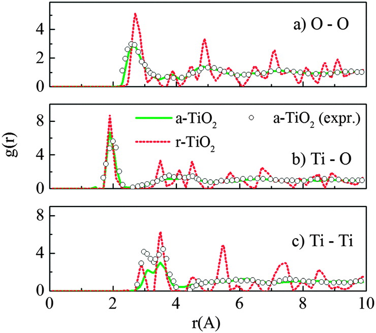 | ||
| Fig. 1 Radial distribution functions g(r) for (a) O–O, (b) Ti–O and (c) Ti–Ti pairs of the amorphous (a-TiO2) and rutile (r-TiO2) models at 300 K, using the Matsui–Akaogi force field. The experimental data for sputtered TiO2 amorphous layers were taken from ref. 15. | ||
It was seen that the amorphous TiO2 model consists of staggered chains of Ti-centered octahedra sharing either the edge or the corner (Fig. 2c), i.e. the local Ti–O bonding is preserved. In other words, most of Ti is surrounded by six O atoms and each O commonly has three Ti neighbors. However, there is a certain amount of Ti with 5-fold or 7-fold coordination; and similarly, O with a “non-perfect” coordination number (2-fold or 4-fold coordinated), as seen in Fig. 2. This observation was also previously reported from both computational and experimental measurements.13,15,27,40 In addition, further charge analysis by the Bader method41,42 based on DFT + U calculations revealed that the strong charge transfer between Ti cations and O anions is preserved, and this could be the driving force for preservation of the nearest neighbor Ti–O bonding in the amorphous phase.
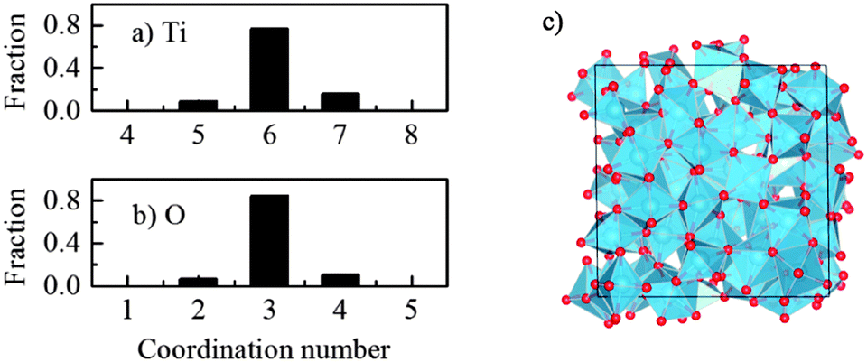 | ||
| Fig. 2 Coordination number distribution in the amorphous TiO2 model for (a) titanium and (b) oxygen. The cutoff distance for calculating the neighbors r = 2.6 Å. (c) Final relaxed structure of the amorphous TiO2 (obtained from “melt-and-quench” of the 216-atom rutile system), after atomic relaxation using DFT + U. Red sphere – O, blue – Ti. | ||
The calculations on electronic properties of amorphous TiO2 to this end will be performed on the sample obtained from “melt-and-quench” of a rutile supercell (216 atoms), and for the comparison purpose we used two rutile supercells (with 72 and 216 atoms) to study the electronic properties of the TiO2 crystal. Interestingly, the amorphous TiO2 has a clean band gap (Fig. 3), despite the noticeable structural disorder and non-perfect coordination numbers. This is in contrast with the situation in covalent bonded semiconductors, e.g. GaAsN, where a good amorphous structure is difficult to obtain from molecular dynamics simulation, and non-perfect coordination often leads to band gap states.12 This is also consistent with the conclusion from recent theoretical studies that amorphization introduces deep defect states or carrier-recombination centers in covalent systems but not in ionic materials.43 Similar to crystalline TiO2, the conduction band edge in amorphous structure is derived from Ti 3d orbitals and the valence band maximum consists mostly of the O 2p orbitals. To correct the well-known band gap underestimation by GGA, we performed additional calculations with the non-local hybrid functional (HSE06),24 using the pre-optimized structure from the DFT + U method. The band gap of amorphous TiO2 obtained by the HSE06 method is 3.2 eV, which agrees with experimental data reported for its optical gap between 3.2–3.4 eV.44–47 The hybrid calculation for the rutile band gap (2.91 eV) is also close to that from experimental measurements (3.06 eV).48Fig. 3, nevertheless, indicates that the charge delocalization of the band edges is strongly affected by the long-range structural disorder. Both the top of the valence band and the bottom of the conduction band are confined to certain regions in the supercell, instead of being delocalized all over the cell. This is consistent with theoretical observations previously reported for amorphous TiO2 and GaN.10,11,17,49 Also, it is believed that the characterization of the band edges would play an essential role in establishing the polaronic or band-like natures of charge carriers.50
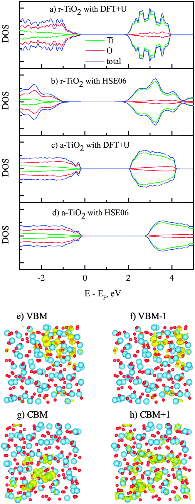 | ||
| Fig. 3 (a–d) Density of states of rutile and amorphous TiO2 calculated using DFT + U and HSE06. (e–h) Band decomposed wave function isosurfaces of the band edge states in amorphous TiO2 (results displayed for DFT + U). | ||
3.2 Trapping of holes and the polaronic states in amorphous TiO2
The hole in the defect-free system is simulated by removing one electron from the valence band maximum, while the charge neutrality is maintained by a compensating uniform charge background. Despite the localization of VBM as seen in Fig. 3, this free hole, without the structural re-optimization, still spreads out over a major part of the supercell and no mid-gap state was induced (Fig. 4a). When the structural relaxation is allowed, we found that the hole polaron could be formed quite naturally (without the help of initial lattice displacement) and this gives rise to a clear mid-gap state of approximately 0.6 eV above the valence band (Fig. 4c). Generally in crystals, the localization of charge carriers requires an initial structural perturbation in order to break the symmetry and trigger the polaronic trapping; otherwise the lattice relaxation will end up in a local minimum with the free (delocalized) charge carrier.51–53 | ||
| Fig. 4 (a) Density of states for amorphous and rutile TiO2 with a hole in the supercell (one electron is removed from the volume of the supercell): (a) a-TiO2 before the lattice relaxation, (b) r-TiO2 before the lattice relaxation, (c) a-TiO2 after the lattice relaxation, and (d) r-TiO2 after the lattice distortion and subsequent optimization. The insets show the charge density isosurfaces of the hole states in corresponding systems. The blue sphere denotes Ti and the red sphere – O. | ||
In crystalline TiO2 such as rutile and anatase, it is expected that the deep trapping of the charge carriers, if formed, is usually located on single Ti or O, subsequently forming small polarons.3,22,32 The self-trapped hole in the amorphous phase, as seen in Fig. 4c however, could be localized on several O anions, instead of a single O. In other words, there could be a tendency for large hole polarons to form in the amorphous phase. This of course is aided by the original localization of the VBM state in the amorphous phase before atomic relaxation. In a way, the exact definition of the polaron state is a bit blurred here due to the lack of a true extended state even before atomic relaxation. The existence of this “molecular polaron” (weak polaron) has been reported by either theoretical investigations or experimental measurements in several oxides, including anatase TiO2, doped BaTiO3, KNbO3 and SiO2.54–57
The self-trap energy EST of the polaronic hole is defined as the difference between the initial atomic structure energy (with the free/delocalized hole) and the energy of atomic relaxed system with the localized hole. Using the same U parameter in the DFT + U calculations (U[Tid] = 4.2), the self-trap energies of the hole in the amorphous and rutile TiO2 were calculated as −1.3 and +0.5 eV, respectively. The positive value obtained for rutile, within this framework, suggests that the localization of the hole could be one of local minima instead of the global one. With the help of structural distortion to break the symmetry, the free (delocalized) charge can be forced to partially localize at some O atom and this induces a tail state on the valence band (Fig. 4d). In a separate calculation, further incorporation of U[Op] = 5.253 yields a stronger localization of hole for the rutile crystal but the self-trap energy is still slightly positive (+85 meV). However, some theoretical studies have shown the formation of hole polaron both at the surface and in the doped bulk rutile TiO2.58–61 But it was also proposed that acceptor states could be deep in anatase but are shallow in rutile;21,62 in addition, the self-trapped and delocalized hole states could be energetically comparable.59,63 Our DFT + U results here are supportive of the shallow rutile polaron hypothesis.
Our calculations therefore have suggested the trend that the self-trap energy of holes in the amorphous structure is much larger than its rutile counterpart. There could be several reasons for this observation. Firstly, the VBM of a-TiO2 before atomic relaxation is somehow already localized. Thus, further localization will not cause much kinetic energy due to wave function confinement.53 Secondly, the chemical bonds near the VBM state might not be as strong as those in the crystal structure. The relative imperfect and hence loose chemical bonds result in more pronounced atomic relaxations, therefore deepening the trapping energy. The effective volume of the wave function (Vhole = 1/∫|ψhole(r)|4d3r) for the hole states before and after the atomic relaxations is 66.2 and 5.6 Å3, respectively. This indicated a significant localization of charge as a result of structural optimization. The hole wave functions are also shown as insets in Fig. 4.
3.3 Oxygen vacancy defect states in amorphous TiO2
We have calculated the oxygen vacancy formation energy VO0 in different TiO2 phases (in the oxygen-rich condition) and the comparison is presented in Table 1. It was shown that the formation of VO0 in the amorphous structure is energetically much more favorable. Surprisingly, the formation energy in a-TiO2 could be lower by as much as 3 or 4 eV, compared to that in crystalline TiO2. This is probably due to the intrinsic bonding frustration in the amorphous structure.64 However, the ΔH(VO0) value could be different from site to site. We observed that the oxygen atoms, at which the VBM state is localized (as shown in Fig. 3d), are the most favorable sites for vacancy formation (which are the values presented in Table 1). Consider however that our supercell consists of only 216 atoms (144 oxygen sites), such favorable sites are rather abundant. Our calculations also indicated that the formation of the bi-vacancy (two vacancies at nearest neighboring sites) could be energetically favorable, compared to two separate vacancies, in the TiO2 crystal (rutile). However, it is not necessarily the case in a-TiO2, where we found a positive binding energy of vacancies to form the bi-vacancy.| Rutile | Anatase | Brookite | Amorphous | |
|---|---|---|---|---|
| ΔH(VO0), eV | 5.59 | 4.42 | 5.20 | 1.35 |
The calculated O vacancy formation energies ΔH(VOq) for different charge states q in the amorphous and rutile supercells are plotted in Fig. 5 as a function of Fermi energy (shifting from the valence band maximum, EF = 0). It indicated that the oxygen vacancy could exist in three charge states (neutral, +1 and +2) in amorphous TiO2, as well as in rutile. At Fermi levels near the VBM, the positively charged VO+1 and VO+2 could form spontaneously in amorphous TiO2. When the Fermi energy increases, the formation energy of the positively charged defect increases, until the transaction to the neutral state occurs. The transitions from VO0 to VO+1 (denoted as ε0/+1) and from VO+1 to VO+2 (ε+1/+2) were all observed within the band gap (Fig. 5) for both phases (amorphous and rutile). In the amorphous structure, these turning points (both ε0/+1 and ε+1/+2) are deeper below the CBM, compared to those in the rutile.
 | ||
| Fig. 5 Formation energy of oxygen vacancy at different charge states in: (a) amorphous and (b) rutile titanium dioxide (DFT + U calculations). The oxygen-rich conditions were used in the eqn (1). | ||
Herein we present further analysis on the mid-gap states induced by vacancies VO0,VO+1 and VO+2 in Fig. 6. The removal of one neutral oxygen results in two unbound electrons and it was commonly accepted that these excess electrons are localized on surrounding Ti sites and subsequently form Ti3+ in rutile and anatase, i.e. the (neutral) oxygen vacancy comes in complex with two Ti3+ sites.64,65 The corresponding Ti3+ peaks have been observed at 1.2 eV and 0.75 eV below the CBM in rutile.5 Similarly, deep traps 0.9 eV and 0.5 eV below the conduction band edge, identified with transient spectroscopy, were also reported in anatase.66 According to our DFT + U calculations, the mid-gap states in reduced amorphous TiO2 are located at 1.9 and 1.6 eV below the conduction band minimum (Fig. 6b). The locations of these impurity states within the band gap were further confirmed by performing additional HSE06 calculations (for the correction of the band gap) and it showed that the peaks are at 1.7 and 1.6 eV below the CBM, consistent with the DFT + U results. Thus, our calculated amorphous TiO2 neutral O vacancy levels are deeper from the conduction band than the experimentally measured levels in rutile and anatase. However, this is consistent with the fact that our calculated VO0/VO+1 transition level in amorphous TiO2 is lower than that of rutile as shown in Fig. 5 counting from the conduction band.
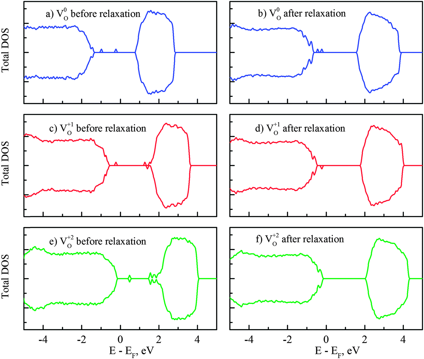 | ||
| Fig. 6 Density of states (from DFT + U calculations) of the amorphous TiO2 with the oxygen vacancy in different charge states (before and after structural relaxation): (a, b) neutral vacancy, (c, d) vacancy with charge +1 and (e, f) vacancy with charge +2. | ||
If one occupied impurity electron is removed from the system, i.e. the vacancy now becomes VO+1, the impurity states are separated into two states (one occupied and one empty) with a significant energy gap, as displayed in Fig. 6(c) and (d). The unoccupied level is initially located near the conduction band edge if the VO0 state atomic position is used. After atomic relaxation, the empty state moves up in energy and subsequently merges into the conduction band. Meanwhile, the other occupied state stays at 1.9 eV below the CBM. When both electrons are removed together with the oxygen VO+2, these unoccupied states could be seen in the band gap before the relaxation (Fig. 6e). After the structural relaxation, these (empty) energy states are shifted up and merge with the conduction band and therefore return a clear band gap again. This finding is consistent with other oxides or ionic systems: when an ion is removed in its normal valence state (e.g., O2−), no gap state will exist after the structural relaxation.67
3.4 The defect induced hole conductivity in amorphous TiO2
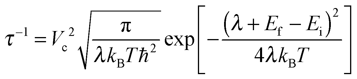
After the investigation of the structure, polarons and defect states in amorphous TiO2, we now like to discuss the possible mechanisms of hole conduction in the “leaky” amorphous TiO2 protection layer as reported in the recent discovery by Hu et al.23 In fact, the mechanism of the hole conductivity reported in ref. 23 was not clear. It was suspected that N and C impurities, or other defects related to amorphous TiO2 might play a role. One interesting phenomenon is the existence of a weak density of state peak in the X-ray induced electron emission spectrum.23 This peak is at approximately 1.5 eV above the top of the valence band and in the order of 1% compared to the main peak. The reported secondary-ion mass spectrometry data counts for N and C indicate that they might be four orders of magnitudes smaller than that of Ti, thus perhaps too dilute to account for the 1% electronic density of state. Furthermore, it was reported that23 the hole conduction was no longer observed after thermo annealing (also disappeared is the 1% defect density of state), while the N and C contents remain constant (although the crystallinity/amorphousness of the system might also have changed). All these prompt us to propose that the O vacancy in amorphous TiO2 could be one hole conduction channel. Due to the relatively low formation energy as shown in Table 1 and Fig. 5a, and the kinetic process in sputtering such thin film, the neutral O vacancy can be formed, perhaps with a concentration of around 1%. Many of the oxides can have such small off-stoichiometry, especially the oxygen deficit. Since the TiO2 amorphous thin film is n-type, the O vacancy should be in the neutral state. Our calculation shows that (Fig. 6b) such O vacancies can produce occupied impurity density of states above the VBM. Note that, our calculated impurity states shown in Fig. 6b are too close to the VBM compared to the X-ray photoelectron emission measured impurity density of state (which is about 1.5 eV above the VBM23). However, when we compare such an X-ray induced electron emission spectrum, we should really compare the average of the density of states of VO0 and VO1+ (before and after the electron has been emitted, and both at the VO0 atomic structure); in other words, taking the average of the higher peaks in Fig. 6b and c. As a result, the averaged peak should be around 1.5 eV above VBM, hence in good agreement with the experimental data (one can also take the total energy difference before and after removing one electron from the impurity state with the VO0 atomic structure, such a result is usually very close to the above averaging procedure). As for the disappearance of the impurity state and the hole conductivity after thermal annealing, one natural interpretation is the filling of such O vacancies during thermal annealing. In addition, one might also consider the direct polaron transport without the O vacancy; however, the polaron level might be too close to the VBM level. Besides, there is no defect impurity state within the gap without O vacancy, therefore inconsistent with the X-ray photoelectron emission data.In order to evaluate the extent of hole conductivity resulted from the O vacancies, we use the Marcus theory to study the hole hopping rate from one O vacancy to a neighboring one. Since we assume the vacancy concentration at about 1% (which is approximately the same amount as in our defect amorphous supercell), we can use the hopping rate from one O vacancy to its periodic image to estimate this transfer rate. The charge transfer rate 1/τ, according to the Marcus theory, could be calculated as follows:68,69
 | (2) |
| μ = 6eb2/(τkBT) | (3) |
The calculated values of τ and μ for hole transfer via the O-defect channel in amorphous TiO2 at room temperature are tabulated in Table 2. According to Marcus theory, the transition rate depends sensitively on the reorganization energy λ. Here the λ due to the hole charge transfer is calculated as: EN−1(R(VO0)) − EN−1(R(VO+1)) + EN(R(VO1+)) − EN(R(VO0)), where EN−1 and EN are energies for N − 1 electron and N electron (neutral) systems. R(VO0) and R(VO0) indicate the energies that are calculated at the relaxed atomic structures of the neutral and 1 + charged O vacancies, respectively. Our calculated λ and the resulting μ from the DFT + U (U = 4.2 eV) and the DFT (GGA) results are very different. The DFT + U λ is 0.9 eV larger than the DFT result. This is because the DFT + U has a tendency to overestimate the wave function localization, while plain DFT tends to make the wave function delocalized. In this regard, the HSE06 should be a function that is more reliable. Therefore, we have also performed HSE06 calculations. However, it is quite computationally expensive to obtain the relaxed atomic structures using HSE06 for several-hundred-atom systems, thus we have estimated this λ using formula: EN−1(R′(VO0)) − EN−1(R′(VO+1)) + EN(R′(VO1+)) − EN(R′(VO0)), and called the result λ* as indicated in Table 2. Here the R′ is the relaxed atomic position taken from DFT + U calculations, while the energy EN−1 and EN are evaluated using self-consistent HSE06 calculations. To test the accuracy of this procedure, we have used the same formula to calculate DFT λ, and the resulting DFT λ* and hole mobility are very similar to the original DFT values (Table 2). As a matter of fact, this can be a rather general procedure to evaluate the reorganization energy of a charge transfer process under an expensive functional using the atomic positions of another inexpensive calculation. To illustrate why this procedure is reliable, we offer the following explanation.
| Calculation method | λ (eV) | V c (meV) | τ (ns) | μ (cm2 V−1 s−1) |
|---|---|---|---|---|
| DFT + U | 1.14 | 1.5 | 1856 | 2.5 × 10⁻⁶ |
| DFT | 0.23 | 2.6 | 0.04 | 1.1 × 10⁻¹ |
| DFT* | 0.24 | 2.4 | 0.05 | 0.9 × 10⁻¹ |
| HSE06* | 0.79 | 2.3 | 23 | 2.0 × 10⁻⁴ |
A schematic diagram for how to calculate the relaxation energy λ in a charge transfer problem is displayed in Fig. 7. Note that this diagram is slightly different from the conventional Marcus diagram, since when the hole hops from the EN−1 system to the EN one, both systems will relax and contribute to the reorganization energy. Assuming both EN−1 and EN have a quadratic form of ½κ(R − R0)2 at their corresponding minimum points R0, the reorganization energy can be calculated as (Fig. 7a):
| λ = EN−1(B) − EN−1(C) + EN(D) − EN(A) = κΔR2 | (4) |
 | ||
| Fig. 7 Schematic diagram for calculations of hole-transfer reorganization energy λ. The EN−1 and EN correspond to states with and without a hole (neutral charge), respectively. (a) Both final configurations before and after charge transfer are the ground states. ΔR is the structural relaxation due to the presence of one hole. This scheme corresponds to cases of fully relaxed structures for a given energy functional, as used in regular DFT and DFT + U calculations. (b) All configurations before and after charge transfer are shifted from the ground states by a value δ. This scheme corresponds to cases of DFT* and HSE06* in Table 2, in which the pre-optimized structures from DFT + U are used for the energy calculations. | ||
| λ* = EN−1(B′) − EN−1(C′) + EN(D′) − EN(A′) = ½κ[(ΔR + δ)2 − δ2] + ½κ[(ΔR − δ)2] = κΔR2 | (5) |
Thus λ and λ* come out to be identical.
Our calculated λ* by the above HSE06* approach is 0.79 eV and the state-state coupling Vc is about 2.3 meV. As a result, the hole hopping time τ is 23 ns. This τ yields a mobility of 2.0 × 10⁻⁴ cm2 V−1 s−1 at room temperature. Unfortunately, experimental data on the mobility and hole transfer even in crystal TiO2 are quite limited.70 The hole mobility of undoped rutile TiO2 measured by Odier et al. based on the Hall effect method is 0.1 (cm2 V−1 s−1) at 1300 K.71 Recently, Deskins et al.54 have calculated the hole polaron mobility in rutile TiO2 to be 0.16 (cm2 V−1 s−1) at 1300 K, and 5.1 × 10⁻³ at 298 K. Thus, our amorphous TiO2 mobility via the O vacancy channel is approximately only one order of magnitude smaller than the corresponding bulk crystal mobility. We believe that might be mobile enough to provide the hole leaky channel in the amorphous TiO2 protection layer. We also note that there is a possibility to lower the total energy (raise the hole level) a little bit after each charge transfer (Ef − Ei < 0 in eqn (2)). This can significantly enhance the transition rate at the expense of losing some potential after the charge transport.
4. Conclusions
In summary, we have investigated the possible mechanism of hole conduction in amorphous TiO2via defect states. We have proposed that the amorphization and the favorable formation of the oxygen vacancy in a-TiO2 could promote the hole transport. Specifically, the O defect state could serve as a hole transfer channel at about 1–1.5 eV above the VBM and be responsible for the good conductivity in the recently discovered “leaky” ALD-TiO2 coating layer for water-splitting photoanodes.23In the amorphous TiO2 structure, the nearest neighbor Ti–O bonding and local octahedral configurations are preserved. The long-range disorder and imperfect coordination of Ti and O do not induce defect states in the band gap but have effects on the localization of band edge states. The trapping of holes can occur naturally without initial lattice distortion. The structural disorder upon amorphization results in a substantial reduction of O vacancy formation energy; as a result, the O vacancy in amorphous TiO2 could be much more abundant than its crystal counterparts. The neutral O vacancy is a deep donor in amorphous TiO2. The calculated O vacancy photoemission peak should be in the range of 1–1.5 eV above the edge of the valence band, in good agreement with the experimentally measured X-ray emission data for the impurity states.23 At around 1% O vacancy concentration, the estimated hole mobility via the O vacancy channel is about 10 times lower than the hole polaron mobility in bulk rutile TiO2. Thus, we believe the O vacancy is capable of providing a “leaky” channel in the middle of the band gap for the a-TiO2 protection layer reported in Hu et al.23
Conflicts of interest
The authors declare no competing financial interests.Acknowledgements
We would like to thank Dr S. Hu for very helpful discussions. This material is based on the work performed by the Joint Center for Artificial Photosynthesis, a DOE Energy Innovation Hub, supported through the Office of Science of the U.S. Department of Energy under Award number DE-SC0004993. We use the resource of National Energy Research Scientific Computing center (NERSC) located in the Lawrence Berkeley National Laboratory.References
- A. Fujishima and K. Honda, Nature, 1972, 238, 37–38 CrossRef CAS.
- X. Chen and S. S. Mao, Chem. Rev., 2007, 107, 2891–2959 CrossRef CAS PubMed.
- B. J. Morgan and G. W. Watson, Phys. Rev. B: Condens. Matter Mater. Phys., 2009, 80, 233102 CrossRef.
- M. Landmann, E. Rauls and W. G. Schmidt, J. Phys.: Condens. Matter, 2012, 24, 195503 CrossRef CAS PubMed.
- D. C. Cronemeyer, Phys. Rev., 1959, 113, 1222–1226 CrossRef CAS.
- C. Di Valentin, G. Pacchioni and A. Selloni, Phys. Rev. B: Condens. Matter Mater. Phys., 2004, 70, 085116 CrossRef.
- B. J. Morgan, D. O. Scanlon and G. W. Watson, J. Mater. Chem., 2009, 19, 5175–5178 RSC.
- S. K. Deb, Solid State Commun., 1972, 11, 713–715 CrossRef CAS.
- V. A. Bakaev and W. A. Steele, Langmuir, 1992, 8, 1372–1378 CrossRef CAS.
- M. Landmann, T. Kohler, S. Koppen, E. Rauls, T. Frauenheim and W. G. Schmidt, Phys. Rev. B: Condens. Matter Mater. Phys., 2012, 86, 064201 CrossRef.
- B. Prasai, B. Cai, M. K. Underwood, J. P. Lewis and D. A. Drabold, J. Mater. Sci., 2012, 47, 7515–7521 CrossRef CAS.
- E. B. Kandemir, B. Gonul, G. T. Barkema, K. M. Yu, W. Walukiewicz and L. W. Wang, Comput. Mater. Sci., 2014, 82, 100–106 CrossRef PubMed.
- H. Z. Zhang, B. Chen, J. F. Banfield and G. A. Waychunas, Phys. Rev. B: Condens. Matter Mater. Phys., 2008, 78, 214106 CrossRef.
- M. Kanna and S. Wongnawa, Mater. Chem. Phys., 2008, 110, 166–175 CrossRef CAS PubMed.
- V. Petkov, G. Holzhuter, U. Troge, T. Gerber and B. Himmel, J. Non-Cryst. Solids, 1998, 231, 17–30 CrossRef CAS.
- R. D. Eithiraj and K. R. Geethalakshmi, Chem. Phys. Lett., 2013, 585, 138–142 CrossRef CAS PubMed.
- K. K. Ghuman and C. V. Singh, J. Phys.: Condens. Matter, 2013, 25, 475501 CrossRef PubMed.
- T. Kohler, M. Turowski, H. Ehlers, M. Landmann, D. Ristau and T. Frauenheim, J. Phys. D: Appl. Phys., 2013, 46, 325302 CrossRef.
- Z. Y. Zhang and P. A. Maggard, J. Photochem. Photobiol., A, 2007, 186, 8–13 CrossRef CAS PubMed.
- S. D. Standridge, G. C. Schatz and J. T. Hupp, Langmuir, 2009, 25, 2596–2600 CrossRef CAS.
- P. Deak, B. Aradi and T. Frauenheim, Phys. Rev. B: Condens. Matter Mater. Phys., 2011, 83, 155207 CrossRef.
- S. Y. Chen and L. W. Wang, Phys. Rev. B: Condens. Matter Mater. Phys., 2014, 89, 014109 CrossRef.
- S. Hu, M. R. Shaner, J. A. Beardslee, M. Lichterman, B. S. Brunschwig and N. S. Lewis, Science, 2014, 344, 1005–1009 CrossRef CAS PubMed.
- J. Paier, M. Marsman, K. Hummer, G. Kresse, I. C. Gerber and J. G. Angyan, J. Chem. Phys., 2006, 125, 249901 CrossRef PubMed.
- S. L. Dudarev, G. A. Botton, S. Y. Savrasov, C. J. Humphreys and A. P. Sutton, Phys. Rev. B: Condens. Matter Mater. Phys., 1998, 57, 1505–1509 CrossRef CAS.
- M. Matsui and M. Akaogi, Mol. Simul., 1991, 6, 239–244 CrossRef.
- V. V. Hoang, Phys. Status Solidi B, 2007, 244, 1280–1287 CrossRef CAS.
- W. Kohn and L. J. Sham, Phys. Rev., 1965, 140, 1133–1138 CrossRef.
- G. Kresse and J. Furthmuller, Phys. Rev. B: Condens. Matter Mater. Phys., 1996, 54, 11169–11186 CrossRef CAS.
- P. E. Blochl, Phys. Rev. B: Condens. Matter Mater. Phys., 1994, 50, 17953–17979 CrossRef.
- J. P. Perdew, K. Burke and M. Ernzerhof, Phys. Rev. Lett., 1996, 77, 3865–3868 CrossRef CAS.
- B. J. Morgan and G. W. Watson, Phys. Rev. B: Condens. Matter Mater. Phys., 2010, 82, 144119 CrossRef.
- B. J. Morgan and G. W. Watson, J. Phys. Chem. C, 2009, 113, 7322–7328 CAS.
- P. M. Kowalski, M. F. Camellone, N. N. Nair, B. Meyer and D. Marx, Phys. Rev. Lett., 2010, 105 Search PubMed.
- H. J. Monkhorst and J. D. Pack, Phys. Rev. B: Solid State, 1976, 13, 5188–5192 CrossRef.
- S. Lany and A. Zunger, Phys. Rev. B: Condens. Matter Mater. Phys., 2009, 80, 085202 CrossRef.
- S. Y. Chen and L. W. Wang, Appl. Phys. Lett., 2011, 99, 222103 CrossRef PubMed.
- K. A. Persson, B. Waldwick, P. Lazic and G. Ceder, Phys. Rev. B: Condens. Matter Mater. Phys., 2012, 85, 235438 CrossRef.
- J. A. Pople, M. Headgordon, D. J. Fox, K. Raghavachari and L. A. Curtiss, J. Chem. Phys., 1989, 90, 5622–5629 CrossRef CAS PubMed.
- K. Kaur, S. Prakash, N. Goyal, R. Singh and P. Entel, J. Non-Cryst. Solids, 2011, 357, 3399–3404 CrossRef CAS PubMed.
- R. Bader, Atoms in Molecules: A Quantum Threory, Oxford University Press, New York, 1990 Search PubMed.
- G. Henkelman, A. Arnaldsson and H. Jonsson, Comput. Mater. Sci., 2006, 36, 354–360 CrossRef PubMed.
- H. X. Deng, S. H. Wei, S. S. Li, J. B. Li and A. Walsh, Phys. Rev. B: Condens. Matter Mater. Phys., 2013, 87, 125203 CrossRef.
- S. B. Amor, L. Guedri, G. Baud, M. Jacquet and M. Ghedira, Mater. Chem. Phys., 2003, 77, 903–911 CrossRef.
- H. Takikawa, T. Matsui, T. Sakakibara, A. Bendavid and P. J. Martin, Thin Solid Films, 1999, 348, 145–151 CrossRef CAS.
- Z. W. Zhao, B. K. Tay, S. P. Lau and G. Q. Yu, J. Cryst. Growth, 2004, 268, 543–546 CrossRef CAS PubMed.
- M. Zhang, G. Q. Lin, C. Dong and L. S. Wen, Surf. Coat. Technol., 2007, 201, 7252–7258 CrossRef CAS PubMed.
- A. Welte, C. Waldauf, C. Brabec and P. J. Wellmann, Thin Solid Films, 2008, 516, 7256–7259 CrossRef CAS PubMed.
- B. Cai and D. A. Drabold, Phys. Rev. B: Condens. Matter Mater. Phys., 2011, 84, 075216 CrossRef.
- M. D. Johannes, K. Hoang, J. L. Allen and K. Gaskell, Phys. Rev. B: Condens. Matter Mater. Phys., 2012, 85, 115106 CrossRef.
- J. B. Varley, A. Janotti, C. Franchini and C. G. Van de Walle, Phys. Rev. B: Condens. Matter Mater. Phys., 2012, 85, 081109 CrossRef.
- S. P. Ong, Y. F. Mo and G. Ceder, Phys. Rev. B: Condens. Matter Mater. Phys., 2012, 85, 081105 CrossRef.
- A. Janotti, C. Franchini, J. B. Varley, G. Kresse and C. G. Van de Walle, Phys. Status Solidi RRL, 2013, 7, 199–203 CrossRef CAS.
- N. A. Deskins and M. Dupuis, J. Phys. Chem. C, 2009, 113, 346–358 CAS.
- T. Varnhorst, O. F. Schirmer, H. Krose, R. Scharfschwerdt and T. W. Kool, Phys. Rev. B: Condens. Matter Mater. Phys., 1996, 53, 116–125 CrossRef CAS.
- E. A. Kotomin, R. I. Eglitis, A. V. Postnikov, G. Borstel and N. E. Christensen, Phys. Rev. B: Condens. Matter Mater. Phys., 1999, 60, 1–5 CrossRef CAS.
- S. Sicolo, G. Palma, C. Di Valentin and G. Pacchioni, Phys. Rev. B: Condens. Matter Mater. Phys., 2007, 76, 075121 CrossRef.
- A. Iwaszuk and M. Nolan, J. Phys.: Condens. Matter, 2011, 23, 334207 CrossRef PubMed.
- P. Zawadzki, A. B. Laursen, K. W. Jacobsen, S. Dahl and J. Rossmeisl, Energy Environ. Sci., 2012, 5, 9866–9869 CAS.
- Y. F. Ji, B. Wang and Y. Luo, J. Phys. Chem. C, 2014, 118, 1027–1034 CAS.
- A. Stashans and S. Bermeo, Chem. Phys., 2009, 363, 100–103 CrossRef CAS PubMed.
- T. Yamamoto and T. Ohno, Phys. Chem. Chem. Phys., 2012, 14, 589–598 RSC.
- P. Zawadzki, K. W. Jacobsen and J. Rossmeisl, Chem. Phys. Lett., 2011, 506, 42–45 CrossRef CAS PubMed.
- A. Janotti, J. B. Varley, P. Rinke, N. Umezawa, G. Kresse and C. G. Van de Walle, Phys. Rev. B: Condens. Matter Mater. Phys., 2010, 81, 085212 CrossRef.
- A. Malashevich, M. Jain and S. G. Louie, Phys. Rev. B: Condens. Matter Mater. Phys., 2014, 89, 075205 CrossRef.
- T. Miyagi, M. Kamei, T. Mitsuhashi and A. Yamazaki, Appl. Phys. Lett., 2003, 83, 1782–1784 CrossRef CAS PubMed.
- D. Zherebetskyy and L.-W. Wang, Adv. Mater. Interfaces, 2014, 1300131, DOI:10.1002/admi.201300131.
- R. A. Marcus, Rev. Mod. Phys., 1993, 65, 599–610 CrossRef CAS.
- K. Tarafder, Y. Surendranath, J. H. Olshansky, A. P. Alivisatos and L. W. Wang, J. Am. Chem. Soc., 2014, 136, 5121–5131 CrossRef CAS PubMed.
- T. Bak, J. Nowotny, M. Rekas and C. C. Sorrell, J. Phys. Chem. Solids, 2003, 64, 1069–1087 CrossRef CAS.
- P. Odier, J. F. Baumard, D. Panis and A. M. Anthony, J. Solid State Chem., 1975, 12, 324–328 CrossRef CAS.
Footnote |
| † Electronic supplementary information (ESI) available. See DOI: 10.1039/c4cp04209c |
| This journal is © the Owner Societies 2015 |