Conversion of porous anodic Al2O3 into freestanding, uniformly aligned, multi-wall TiO2 nanotube arrays for electrode applications†
John D. Berrigan‡a, Taylor McLachlan‡a, James R. Deneaultb, Ye Caia, Tae-Sik Kangb, Michael F. Durstockb and Kenneth H. Sandhage*ac
aSchool of Materials Science and Engineering, and Air Force Center of Excellence on Bio-nano-enabled Inorganic/Organic Nanocomposites and Improved Cognition (BIONIC), Georgia Institute of Technology, 771 Ferst Drive, Atlanta, GA 30332-0245, USA. E-mail: ken.sandhage@mse.gatech.edu
bMaterials and Manufacturing Directorate, Air Force Research Laboratory, Wright-Patterson Air Force Base, OH 45433-7702, USA
cSchool of Chemistry and Biochemistry, Georgia Institute of Technology, 771 Ferst Drive, Atlanta, GA 30332, USA
First published on 8th November 2012
Abstract
A combined conformal coating and gas/solid reaction process has been used for the first time to convert porous anodic alumina templates into robust, freestanding, multi-wall titania nanotube (MWTNT) arrays that resist appreciable nanotube bundling upon drying. A sol–gel infiltration process was first used to apply a thin conformal titania coating to the alumina templates. After selective etching to generate a gap between the template and the titania coating, exposed alumina was converted into nanocrystalline titania via reaction with titanium tetrafluoride gas and then with humid oxygen. After selective dissolution of residual aluminum-bearing phases and drying, freestanding, non-agglomerated, well-aligned MWTNT arrays were generated (i.e., with coating-derived inner titania tubes resting inside reaction-derived outer titania tubes). When incorporated as aligned electrodes in dye-sensitized solar cells, the dye loading and power conversion efficiencies were higher by factors of 2.2 and 1.8, respectively, than for solar cells with single-wall titania nanotube array electrodes. By controlling the conditions used for alumina template formation, sol–gel coating, and gas/solid reaction, this hybrid process may be used to generate robust, uniformly aligned MWTNT arrays with dimensions and functional chemistries tailored for a variety of electrical, optical, chemical, or biochemical applications.
1 Introduction
The open channels and high surface areas of aligned, high-aspect-ratio titania nanotube arrays make these structures attractive for use in a variety of electronic, optical, chemical, and medical devices (e.g., as electrodes in dye-sensitized solar cells and batteries, as flow-through (photo)catalysts, as gas sensors, as functionalized membranes for selective absorption from solutions, and as antibacterial surfaces).1 A number of authors have reported the syntheses of aligned single-wall titania nanotube (SWTNT) arrays via either anodic oxidation of titanium foils2 or the conformal coating of titania onto porous anodic alumina (AAO) templates followed by selective alumina dissolution.3 However, appreciable nanotube bundling and cracking resulting from capillary stresses generated during drying steps (e.g., after rinsing away residual chemicals used in the titanium anodization process, or after selective dissolution of the AAO template from the titania coating) can act to degrade the alignment and structural uniformity of such thin-walled, high-aspect-ratio SWTNT arrays.2b,c,f,3e,f Nanotube agglomeration also creates additional contact points between nanotubes that can lengthen the electron transport path within the nanotube arrays.2fThe purpose of this work is to demonstrate, for the first time, a combined conformal coating and gas/solid reaction method for converting AAO templates into freestanding, well-aligned, thin-walled, high-aspect-ratio titania nanotube arrays that resist such nanotube bundling upon drying. Instead of complete AAO template dissolution after titania deposition, some of the alumina has been converted into titania via gas/solid reactions, in order to enhance the structural rigidity of the resulting multi-wall titania nanotube (MWTNT) arrays. While prior work has shown that gas/solid displacement reactions can be used to convert one oxide into another while retaining the 3-D morphology of the starting oxide,4 such shape-preserving chemical conversion has not yet been applied for the conversion of nanostructured alumina templates into titania. The dye-loading capacities and power conversion efficiencies of dye-sensitized solar cells (DSSCs) containing MWTNT-based electrodes have been compared to DSSCs containing SWTNT-based electrodes generated without the gas/solid reactive conversion process.
2 Experimental methods
As illustrated in Scheme 1, the conversion of (a) AAO templates into MWTNT arrays was conducted via the following steps: (b) deposition of a conformal titania coating onto the walls of the AAO template nanochannels via a wet chemical process; (c) etching to open the channels of the template (to yield flow-through AAO membranes) and to generate space between the AAO nanochannels and the titania coating; (d) partial reactive conversion of AAO into titanium oxyfluoride (TiOF2); (e) reactive conversion of the oxyfluoride into titania (TiO2), and (f) selective dissolution of non-titania phases to yield freestanding, aligned MWTNT arrays.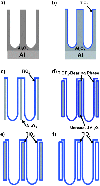 | ||
| Scheme 1 Schematic illustration of the hybrid coating and reaction process used to convert AAO templates into freestanding, aligned MWTNT arrays. | ||
Porous amorphous AAO templates were generated from high-purity (99.999%) aluminum sheets by a two-step anodization process that involved the use of a phosphoric acid-bearing solution with an anodization (pore channel formation) time of 2.5 h at 4 °C and a current density of 6 mA cm−2.3e,f Titania deposition was conducted by double vacuum infiltration of the AAO templates with a solution of titanium(IV) isopropoxide in anhydrous isopropanol (3![[thin space (1/6-em)]](https://www.rsc.org/images/entities/char_2009.gif) :1 weight ratio), followed by hydrolysis in humid air after each infiltration.3e The coated AAO templates were then immersed in an aqueous solution of 0.25 M copper(II) chloride and 6 M hydrochloric acid, followed by immersion in an aqueous solution of 3 M NaOH, to remove the aluminum backing and alumina barrier layer attached to the base of the AAO templates.3f After thermal treatment for 1 h in air at 500 °C, the coated AAO specimens were sealed along with TiF4(s) inside a Ti ampoule within a glovebox purged with high-purity (99.999%) Ar. The specimen-bearing ampoules were then heated to 335 °C for 8 h to generate TiF4(g) (note: the sublimation temperature of TiF4(s) is 285 °C5) that then reacted with the Al2O3 in the template. After removal from the ampoule, the reacted specimens were exposed to flowing, humid oxygen at 250 °C for 8 h, followed by heating to 500 °C for 1.5 h in ambient air. Residual aluminum-bearing phases were then selectively removed by immersion in an aqueous 3 M NaOH solution for 1.5 h to yield freestanding MWTNT arrays. SWTNT arrays were prepared in a similar fashion, but without the halide gas/solid reaction process of the MWTNT arrays.
:1 weight ratio), followed by hydrolysis in humid air after each infiltration.3e The coated AAO templates were then immersed in an aqueous solution of 0.25 M copper(II) chloride and 6 M hydrochloric acid, followed by immersion in an aqueous solution of 3 M NaOH, to remove the aluminum backing and alumina barrier layer attached to the base of the AAO templates.3f After thermal treatment for 1 h in air at 500 °C, the coated AAO specimens were sealed along with TiF4(s) inside a Ti ampoule within a glovebox purged with high-purity (99.999%) Ar. The specimen-bearing ampoules were then heated to 335 °C for 8 h to generate TiF4(g) (note: the sublimation temperature of TiF4(s) is 285 °C5) that then reacted with the Al2O3 in the template. After removal from the ampoule, the reacted specimens were exposed to flowing, humid oxygen at 250 °C for 8 h, followed by heating to 500 °C for 1.5 h in ambient air. Residual aluminum-bearing phases were then selectively removed by immersion in an aqueous 3 M NaOH solution for 1.5 h to yield freestanding MWTNT arrays. SWTNT arrays were prepared in a similar fashion, but without the halide gas/solid reaction process of the MWTNT arrays.
To evaluate the utility of such MWTNTs for the adsorption of functional dyes, and for use as electrodes in DSSCs, the MWTNTs were sinter-bonded at 500 °C for 1 h in air to titania nanoparticle films (1.8 ± 0.2 μm thick) deposited onto fluorine-doped tin oxide (FTO) bearing glass slides.3f A light-harvesting N719 dye (cis-di(thiocyanato)-N-N′-bis(2,2′-bipyridyl-4- carboxylic acid-4′-tetrabutyl-ammonium carboxylate) ruthenium(II)) was introduced by immersion of the MWTNT-bearing FTO glass slides in a 0.3 mM solution of the dye in t-butanol/acetonitrile (1/1 volume) for 24 h. A Pt-coated counter electrode was prepared by depositing an ethanolic solution of 2 mg mL−1 H2PtCl6 onto a FTO-bearing glass slide containing a 1 mm dia. hole, followed by firing at 450 °C for 15 min. A 25 μm thick thermoplast spacer containing a 0.79 cm dia. hole was used to separate the MWTNT-based working electrode from the Pt counter electrode. A redox electrolyte solution, consisting of 0.6 M 1-methyl-3-propyl imidazolium iodide, 0.1 M guanidinium thiocyanate, 0.03 M I2 and 0.5 Mtert-butylpyridine dissolved in a mixture of 85 vol% acetonitrile and 15 vol% valeronitrile, was then vacuum infiltrated into the space between the counter and working electrodes, and the assembly was sealed. DSSCs with working electrodes containing SWTNT arrays were assembled in a similar fashion.
Dye loading measurements were conducted on five MWTNT and five SWTNT electrodes. After rinsing twice in dry acetonitrile, the N719 dye was desorbed from the electrode surfaces by incubation in a solution of 0.1 M NaOH in water/ethanol (1:1 vol. ratio). The concentration of the removed dye in the solution was evaluated by measurement of absorbance at 513 nm using a UV-Vis spectrometer and comparison to a calibration plot prepared using five solutions of known N719 concentration. The amount of N719 adsorbed to the electrodes was normalized to the measured lateral area occupied by the nanotube arrays.
The micro/nanoscale morphologies of the AAO templates and nanotube arrays were evaluated with scanning electron microscopy (1530 FEG SEM, LEO/Zeiss Electron Microscopy, Thornwood, NY) and transmission electron microscopy (JEOL 4000 EX TEM, Japan Electron Optics Laboratory, Tachikawa, Tokyo). The crystal structures of the nanotube arrays were evaluated at room temperature via X-ray diffraction (XRD) analyses conducted with Cu Kα radiation (Alpha-1, PANalytical Corp., Almelo, The Netherlands) and selected area electron diffraction (SAED) analyses in the TEM. Current–voltage (I–V) measurements were conducted under AM 1.5G conditions (Oriel 300 Watt solar simulator, 100 mW cm−2) using an aperture with a measured area of 7.05 mm2.
More detailed descriptions of the experimental steps and analyses are provided in the ESI file.†
3 Results and discussion
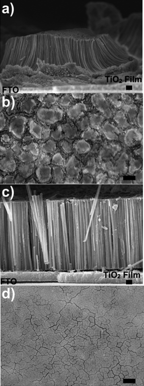
Secondary electron (SE) images of plan and cross-sectional views of specimens at various stages of conversion into MWTNT arrays are shown in Fig. 1 and 2, respectively. The starting AAO templates (Fig. 1a and 2a) possessed well-aligned vertical channels with an average diameter of 207 ± 29 nm and an average height of 13.2 ± 0.4 μm (the ranges refer to ± one standard deviation of measured values). | ||
| Fig. 1 SE images of plan views of specimens obtained at various stages of conversion into MWTNT arrays: (a) a starting AAO template; (b) a coated template after two vacuum infiltrations with the Ti(IV) isopropoxide solution; (c) a coated template after dissolution of the Al backing and Al2O3 barrier layer; (d) a coated template after conversion of exposed Al2O3 into TiO2via reaction with TiF4(g); and (e) a freestanding MWTNT array generated after selective dissolution of non-titania phases from the coated/reacted template. All scale bars correspond to 200 nm. | ||
 | ||
| Fig. 2 SE images of specimen cross-sections obtained at various stages of conversion into MWTNT arrays: (a) a starting AAO template; (b) a coated template after two vacuum infiltrations with the Ti(IV) isopropoxide solution; and (c) a freestanding MWTNT array after reactive conversion of the coated AAO template and selective dissolution of non-titania phases. All scale bars correspond to 200 nm. | ||
After double vacuum infiltration and hydrolysis of the alkoxide precursor, a continuous and conformal titania coating was observed to have formed on the AAO nanochannel walls (Fig. 1b and 2b). Subsequent exposure to an aqueous 3 M NaOH solution (used to remove the alumina backing layer) then introduced space between the AAO and the titania coating (Fig. 1c), so as to expose alumina surfaces for subsequent gas/solid reaction. After thermal treatment at 500 °C in air to allow for organic pyrolysis and crystallization of the sol–gel coating, XRD analysis (Fig. 3a) revealed distinct peaks for only anatase TiO2. Scherrer analysis of these diffraction peaks yielded an average crystallite size of 11 ± 3 nm. The specimens were then allowed to react with TiF4(g) at 335 °C within a sealed Ti ampoule. XRD analysis (Fig. 3b) of such a reacted specimen yielded distinct diffraction peaks for titanium oxyfluoride, TiOF2, as the predominant phase.6 Such TiOF2 formation was consistent with a TiF4(g)/Al2O3(s) reaction of the following type:
| 3TiF4(g) + Al2O3(s) → 3TiOF2(s) + 2AlF3(s) | (1) |
 | ||
| Fig. 3 XRD analyses obtained from: (a) a TiO2-coated AAO template after organic pyrolysis and crystallization for 1 h at 500 °C in ambient air, then (b) reaction with TiF4(g) at 335 °C for 8 h, and (c) further reaction with humid, flowing oxygen at 250 °C for 8 h, followed by thermal treatment at 500 °C for 1.5 h in air. | ||
The absence of diffraction peaks for the AlF3(s) product of this displacement reaction was not surprising, given the glass-forming ability of this fluoride and prior reports of amorphous AlF3(s) formation via low-temperature (≤350 °C) fluorination of Al-bearing precursors.7 The absence of predominant diffraction peaks for anatase TiO2 in Fig. 3b was consistent with the following reaction:
| TiF4(g) + TiO2(s) → 2TiOF2(s) | (2) |
Such reactive conversion of TiO2 into TiOF2 has been previously reported, albeit at ≥550 °C.8 After removal from the ampoules, the reacted specimens were exposed to flowing, humid oxygen at 250 °C to remove fluorine and convert titanium oxyfluoride into titania as per the following previously reported reactions:6
| TiOF2(s) + H2O(g) → TiO2(s) + 2HF(g) | (3a) |
| TiOF2(s) + 1/2O2(g) → TiO2(s) + F2(g) | (3b) |
After further heating at 500 °C for 1.5 h in ambient air, XRD analysis (Fig. 3c) revealed diffraction peaks for only anatase, with an average crystal size (from Scherrer analysis) of 14 ± 5 nm. High resolution transmission electron (HRTE) images of cross-sections of inner and outer titania nanotubes are shown in Fig. 4a and b, respectively. Nanocrystals of 11 ± 3 nm dia. were observed within both inner and outer tube cross-sections, with lattice fringe spacings consistent with anatase (e.g., the 0.352 nm and 0.233 nm spacings of (101) and (112) planes, respectively). SAED analyses obtained within inner and outer tubes (Fig. 4c and d) were also consistent with the presence and absence of anatase TiO2 and TiOF2, respectively. Selective dissolution of the remaining amorphous Al-bearing phases (Al2O3, AlF3) in an aqueous 3 M NaOH solution then yielded freestanding MWTNT arrays (Fig. 1e and 2c).
 | ||
| Fig. 4 (a), and (b) HRTE images of the anatase nanocrystals in the inner (coating-derived) and outer (reaction-derived) nanotubes, respectively, of a fully-converted freestanding MWTNT array. (c), and (d) Corresponding SAED analyses revealing the presence of only the anatase polymorph of TiO2 with the inner and outer nanotubes, respectively. All scale bars correspond to 2 nm. | ||
SE and optical images of cross-sectional and plan views, respectively, of SWTNT and MWTNT arrays bound to FTO-coated glass slides are shown in Fig. 5. Appreciable agglomeration of nanotubes into bundles of roughly 10–30 μm diameter, separated by gaps (microcracks) of up to about 20 μm, was observed within the SWTNT arrays. The MWTNT arrays, however, were much more resistant to such microscale bundling of nanotubes (i.e., gaps of only a few micrometers or less were observed within these arrays), and exhibited a higher degree of vertical nanotube alignment relative to the SWTNT arrays. The enhanced apparent rigidity of the MWTNT arrays avoided the need to use supercritical fluid drying methods to reduce capillary stresses.2f,9 Measurements of the diameters, lengths, and wall thicknesses of the SWTNT and MWTNT arrays, shown in Table 1, were used to calculate values of the “roughness factor” (i.e., the area of the vertical sidewall surfaces of the nanotubes in the array, relative to the horizontal area of the FTO electrode on which the array was placed). The calculated roughness factors for the MWTNT and SWTNT arrays were 282 and 75, respectively (note: details of the roughness factor calculations are provided in the ESI file†). To test whether such increased sidewall area of the MWTNT arrays would result in enhanced dye loading, N719-bearing arrays were immersed in a solvent solution to extract this dye for subsequent analyses by calibrated optical absorption measurements. The average N719 dye loading of five MWTNT arrays was found to be 195 ± 31 nanomoles per cm2, which was 2.2 times greater than the average value for five SWTNT arrays (87 ± 28 nanomoles per cm2). (Note: while some of the dye was loaded onto the titania nanoparticle film used to sinter-bond a given nanotube array to the FTO electrode, similar nanoparticle films were used for both the MWTNT and SWTNT arrays). Hence, in addition to conferring enhanced resistance to nanotube bundling, the multi-wall, nested-tube nature of the coated/reacted arrays allowed for enhanced nanotube sidewall area and significantly higher dye loading.
 | ||
| Fig. 5 (a), and (c) SE images of cross-sectional views and (b), and (d) optical images of plan views of a SWTNT array (in (a) and (b)) and a MWTNT array (in (c) and (d)) bound to FTO-bearing substrates. Scale bars for SE and optical images correspond to 1 μm and 25 μm, respectively. | ||
| Specimen type | Nanotube height (μm) | Inner nanotube thickness (nm); outer dia. (nm) | Outer nanotube thickness (nm); outer dia. (nm) |
|---|---|---|---|
| a Average values indicated, with the error range corresponding to ± one standard deviation. | |||
| SWTNT | 13.2 ± 0.4 | 30 ± 10; 77 ± 20 | — |
| MWTNT | 13.2 ± 0.4 | 34 ± 7; 154 ± 40 | 80 ± 13; 426 ± 75 |
Quasi-one-dimensional structures, such as aligned TiO2 nanotube arrays, have been reported to enhance both electron collection efficiency and light scattering when used as electrodes in DSSCs.10 To demonstrate the utility of aligned MWTNT arrays as working electrodes, five DSSCs were prepared with MWTNT electrodes and five others were prepared with SWTNT electrodes. The performance data for these DSSCs are presented in Table 2, and current–voltage behaviors of SWTNT- and MWTNT-bearing DSSCs are shown in Fig. 6. The best-performing MWTNT-bearing solar cell exhibited a power conversion efficiency of 6.5%, with the worst-performing MWTNT cell possessing an efficiency higher than the best-performing SWTNT cell (4.7% vs. 4.0%). The average values of short circuit current density and power conversion efficiency of the MWTNT-bearing DSSCs were 1.9 and 1.8 times higher, respectively, than for the SWTNT-bearing DSSCs. These values were not far from the 2.2 fold improvement in dye loading of the MWTNT arrays relative to the SWTNT arrays, which, in turn, was consistent with the non-agglomerated, nested nanotube (enhanced roughness factor) structure of the MWTNT arrays. It is worth noting that the average Voc value of these MWTNT array-bearing DSSCs decreased by 18 mV relative to SWTNT-based devices. Such a modest reduction in the Voc value was not surprising, given the larger surface area available for electron–hole recombination in the MWTNT-based devices.
| Parameter | SWTNT devices | MWTNT devices |
|---|---|---|
| a Average values of five devices indicated, with the error range corresponding to ± one standard deviation. | ||
| Jsc (mA cm−2) | 5.6 ± 2.0 | 10.4 ± 1.2 |
| Voc (mV) | 728 ± 29 | 710 ± 30 |
| FF | 0.714 ± 0.04 | 0.714 ± 0.02 |
| η (%) | 3.0 ± 1.0 | 5.50 ± 0.8 |
| Dye adsorption (nmol cm−2) | 87 ± 28 | 195 ± 31 |
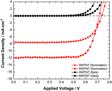 | ||
| Fig. 6 Current–voltage behavior of the best performing SWTNT- and MWTNT-bearing DSSCs in the dark and under AM 1.5G illumination. | ||
The present process may be controllably altered to synthesize robust freestanding arrays of multiwall nanotubes with tailored dimensions and chemistries. The outer diameter, height, and wall thickness of the inner nanotubes can be tailored by adjusting the nanochannel diameter and height of the starting AAO templates (via modification of anodization conditions11) and the number of sol–gel infiltration cycles. The inner diameter of the outer nanotubes can be tailored by controlling the etching process used to open up space between the coating-derived inner nanotubes and the AAO template, whereas the outer nanotube wall thickness can be tailored by controlling the extent of the TiF4(g)/Al2O3 reaction. The inner and outer nanotubes may also possess different functional chemistries via appropriate selections of the sol–gel precursor and the halide used in the gas/alumina reaction. While the synthesis of well-aligned MWTNT arrays for DSSCs has been demonstrated in the present paper, this hybrid (coating and reaction) process may be used to synthesize uniform, well-aligned, multiwalled nanotube structures tailored for use as electrodes, (photo)catalysts, sensors, or filters/absorbers in a host of other applications.
4 Conclusions
A combined sol–gel infiltration and gas/solid displacement reaction method has been used for the first time to convert porous anodic Al2O3 (AAO) into robust, multi-wall nanotube arrays comprised of nanocrystalline anatase TiO2. The nanochannel walls of the AAO template were first coated with a conformal layer of titania via two successive sol–gel vacuum infiltration treatments. Subsequent wet chemical etching was used to remove the aluminum backing and the alumina barrier layer at the base of the template, to generate flow-through membranes as well as to open up a gap between the AAO template and the titania coating. The exposed Al2O3 and TiO2 were allowed to undergo reaction with TiF4(g) at 335 °C to generate TiOF2(s). Reaction of this oxyfluoride compound with humid, flowing oxygen at 250 °C and then air at 500 °C resulted in fluorine removal and conversion into nanocrystalline anatase titania. The resulting multi-wall nanotube array consisted of inner TiO2 nanotubes, derived from the sol–gel coating process, nested within outer TiO2 nanotubes derived from the TiF4(g)/Al2O3(s) reaction process. The enhanced rigidity provided by the reaction-derived outer nanotubes inhibited nanotube agglomeration and microcracking upon drying of the multi-wall titania nanotube (MWTNT) arrays.As expected from estimated values of the roughness factor, these open, uniformly aligned, multi-wall structures were able to absorb 2.2 times more of a light-harvesting N719 dye than single wall titania nanotube (SWTNT) arrays (prepared using a similar sol–gel infiltration process but without the halide gas reaction process). Upon incorporation as electrodes within dye-sensitized solar cells (DSSCs), the MWTNT arrays exhibited average short circuit current density and power conversion efficiency values that were 1.9 and 1.8 times higher, respectively, than for DSSCs containing SWTNT array electrodes.
Although the utility of this hybrid (coating and reaction) process has been demonstrated via the synthesis of robust MWTNT arrays for DSSCs, this process may be used to generate well-aligned oxide nanotube arrays with dimensions and functional chemistries tailored for a variety of other chemical, photochemical, electrochemical, adsorption, and optical applications.
Acknowledgements
This research was supported by the Air Force Office of Scientific Research (Award no. FA9550-09-1-0162, Dr. Charles Lee, Program Manager). Dr. Giorgio Bazzan (Wright-Patterson Air Force Base, OH), Dr. Benjamin Leever (Wright-Patterson Air Force Base, OH), Dr. Richard Vaia (Wright-Patterson Air Force Base, OH), and Dr. Bernard Kippelen (Georgia Institute of Technology) are gratefully acknowledged for their advice and generous donation/use of equipment.References
- (a) K. Zhu, N. R. Neale, A. Miedaner and A. J. Frank, Nano Lett., 2007, 7, 69–74 CrossRef CAS; (b) K. Wang, M. Wei, M. A. Morris, H. Zhou and J. D. Holmes, Adv. Mater., 2007, 19, 3016–3020 CrossRef CAS; (c) S. P. Albu, A. Ghicov, J. M. Macak, R. Hahn and P. Schmuki, Nano Lett., 2007, 7, 1286–1289 CrossRef CAS; (d) D. Wang, Y. Liu, B. Yu, F. Zhou and W. Liu, Chem. Mater., 2009, 21, 1198–1206 CrossRef CAS; (e) H. F. Lu, L. Feng, L. Gang, C. Zhi-Gang, W. Da-Wei, F. Hai-Tao, L. Gao Qing, J. Zhou Hua and C. Hui-Ming, Nanotechnology, 2008, 19, 405504 CrossRef; (f) S. Lin, D. Li, J. Wu, X. Li and S. A. Akbar, Sens. Actuators, B, 2011, 156, 505–509 CrossRef; (g) X. Zhang, A. J. Du, P. Lee, D. D. Sun and J. O. Leckie, Appl. Catal., B, 2008, 84, 262–267 CrossRef CAS; (h) K. C. Popat, M. Eltgroth, T. J. LaTempa, C. A. Grimes and T. A. Desai, Small, 2007, 3, 1878–1881 CrossRef CAS; (i) B. Ercan, E. Taylor, E. Alpaslan and T. J. Webster, Nanotechnology, 2011, 22, 295102 CrossRef; (j) S. Minagar, C. C. Berndt, J. Wang, E. Ivanova and C. Wen, Acta Biomater., 2012, 8, 2875–2888 CrossRef CAS.
- (a) V. Zwilling, E. Darque-Ceretti, A. Boutry-Forveille, D. David, M. Y. Perrin and M. Aucouturier, Surf. Interface Anal., 1999, 27, 629–637 CrossRef CAS; (b) J. M. Macak, H. Tsuchiya and P. Schmuki, Angew. Chem., Int. Ed., 2005, 44, 2100–2102 CrossRef CAS; (c) C. Ruan, M. Paulose, O. K. Varghese, G. K. Mor and C. A. Grimes, J. Phys. Chem. B, 2005, 109, 15754–15759 CrossRef CAS; (d) S. Rani, S. C. Roy, M. Paulose, O. K. Varghese, G. K. Mor, S. Kim, S. Yoriya, T. J. LaTempa and C. A. Grimes, Phys. Chem. Chem. Phys., 2010, 12, 2780–2800 RSC; (e) P. Roy, S. Berger and P. Schmuki, Angew. Chem., Int. Ed., 2011, 50, 2904–2939 CrossRef CAS; (f) K. Zhu, T. B. Vinzant, N. R. Neale and A. J. Frank, Nano Lett., 2007, 7, 3739–3746 CrossRef CAS.
- (a) P. Hoyer, Langmuir, 1996, 12, 1411–1413 CrossRef CAS; (b) C. R. Martin, Science, 1994, 266, 1961–1966 CAS; (c) J. C. Hulteen and C. R. Martin, J. Mater. Chem., 1997, 7, 1075–1087 RSC; (d) M. S. Sander, M. J. Cote, W. Gu, B. M. Kile and C. P. Tripp, Adv. Mater., 2004, 16, 2052–2056 CrossRef CAS; (e) T.-S. Kang, A. P. Smith, B. E. Taylor and M. F. Durstock, Nano Lett., 2009, 9, 601–606 CrossRef CAS; (f) J. D. Berrigan, T.-S. Kang, Y. Cai, J. R. Deneault, M. F. Durstock and K. H. Sandhage, Adv. Funct. Mater., 2011, 21, 1693–1700 CrossRef CAS.
- (a) R. R. Unocic, F. M. Zalar, P. M. Sarosi, Y. Cai and K. H. Sandhage, Chem. Commun., 2004, 795–796 Search PubMed; (b) K. H. Sandhage, R. L. Snyder, G. Ahmad, S. M. Allan, Y. Cai, M. B. Dickerson, C. S. Gaddis, M. S. Haluska, S. Shian, M. R. Weatherspoon, R. A. Rapp, R. R. Unocic, F. M. Zalar, Y. Zhang, M. Hildebrand and B. P. Palenik, Int. J. Appl. Ceram. Technol., 2005, 2, 317–326 CrossRef CAS; (c) S. Shian, Y. Cai, M. R. Weatherspoon, S. M. Allan and K. H. Sandhage, J. Am. Ceram. Soc., 2006, 89, 694–698 CrossRef CAS; (d) S.-J. Lee, S. Shian, Ch.-H. Huang and K. H. Sandhage, J. Am. Ceram. Soc., 2007, 90, 1632–1636 CrossRef CAS.
- I. Barin and G. Platzki, Thermochemical Data of Pure Substances, VCH, Weinheim, Germany, 1989 Search PubMed.
- S. Shian and K. H. Sandhage, J. Appl. Crystallogr., 2010, 43, 757–761 CAS.
- (a) C. M. Baldwin and J. D. Mackenzie, J. Am. Ceram. Soc., 1979, 62, 537–538 CrossRef CAS; (b) C. M. Baldwin, R. M. Almeida and J. D. Mackenzie, J. Non-cryst. Solids, 1981, 43, 309–344 CrossRef CAS; (c) E. Kemnitz, E. Groβ, S. Ruediger and C. S. Shekar, Angew. Chem., Int. Ed., 2003, 42, 4251–4254 CrossRef CAS; (d) S. K. Ruediger, U. Groβ, M. Feist, H. A. Prescott, S. Chandra Shekar, S. I. Troyanov and E. Kemnitz, J. Mater. Chem., 2005, 15, 588–597 RSC; (e) S. Ruediger, G. Eltanany, U. Groβ and E. Kemnitz, J. Sol-Gel Sci. Technol., 2007, 41, 299–311 CrossRef CAS.
- J. H. Moss and A. Wright, J. Fluorine Chem., 1975, 5, 163–167 CrossRef CAS.
- J. R. Deneault, X. Xiao, T.-S. Kang, J. S. Wang, C. M. Wai, G. J. Brown and M. F. Durstock, ChemPhysChem, 2012, 13, 256–260 CrossRef CAS.
- (a) K. Zhu, N. R. Neale, A. Miedaner and A. J. Frank, Nano Lett., 2007, 7, 69–74 CrossRef CAS; (b) J. R. Jennings, A. Ghicov, L. M. Peter, P. Schmuki and A. B. Walker, J. Am. Chem. Soc., 2008, 130, 13364–13372 CrossRef CAS.
- (a) F. Keller, M. S. Hunter and D. L. Robinson, J. Electrochem. Soc., 1953, 100, 411–419 CrossRef CAS; (b) R. C. Furneaux, W. R. Rigby and A. P. Davidson, Nature, 1989, 337, 147–149 CrossRef CAS; (c) H. Masuda, H. Yamada, M. Satoh, H. Asoh, M. Nakao and T. Tamamura, Appl. Phys. Lett., 1997, 71, 2770–2772 CrossRef CAS; (d) O. Jessensky, F. Mueller and U. Goesele, Appl. Phys. Lett., 1998, 72, 1173–1175 CrossRef CAS; (e) A. P. Li, F. Mueller, A. Birner, K. Nielsch and U. Goesele, J. Appl. Phys., 1998, 84, 6023–6026 CrossRef CAS.
Footnotes |
| † Electronic supplementary information (ESI) available: Detailed experimental procedures, additional morphological, phase, and optical characterization (PDF). See DOI: 10.1039/c2ta01015a |
| ‡ These authors contributed equally to this work. |
| This journal is © The Royal Society of Chemistry 2013 |