Low temperature synthesis, optical and photoconductance properties of nearly monodisperse thin In2S3 nanoplatelets
Anuja
Datta
*a,
Devajyoti
Mukherjee
ab,
Sarath
Witanachchi
ab and
Pritish
Mukherjee
ab
aFlorida Cluster for Advanced Smart Sensor Technologies & Department of Physics, University of South Florida, Tampa, Fl 33620, USA. E-mail: datta@usf.edu
bCenter for Integrated Functional Materials & Department of Physics, University of South Florida, Tampa, Fl 33620, USA
First published on 30th October 2012
Abstract
We report on the synthesis of nearly monodisperse In2S3 nanoplatelets ∼7 nm thick by a low temperature polyol process using 1-thioglycerol as the capping chemical. The synthesized nanoplatelets crystallized in bulk tetragonal structure and show preferential crystallographic growth within a range of diameters from ∼75–85 nm. Quantum confinement was observed by spectroscopic analyses with a determined band gap of 3.4 eV. Strong UV luminescence corroborated valence-conduction band transition in these confined nanoplatelets. Room temperature photoconductance measurements performed on the prototype device fabricated from the nanoplatelets revealed noticeable enhancement of conductivity under illumination as compared to the dark condition.
Introduction
The preparation of monodisperse nanocrystals, passivated by organic molecules permits studies to distinguish truly novel properties obtained for nano-scale structures compared to their polydisperse counterparts.1–6 Shape-controlled monodisperse nanocrystals have recently been in focus since building blocks for electronic and optical nano-scale devices often require assembly of nanocrystals with non-spherical morphologies.7–12 In semiconductor materials, quantum confinement allows size-tunability in optical and electrical properties once a critical dimension threshold is attained.13 These effects have been studied in a wide range of materials systems,2,3,7 among which chalcogenides are of particular interest. This interest has been fueled by the high degree of reproducibility and control that is currently available in the fabrication and manipulation of chalcogenide quantum-confined structures.14,15 Among many important chalcogenide semiconductors, In2S3 is a promising optoelectronic material with superior photoconductive properties.16,17 Due to its stability and nontoxicity, the material is also potentially being explored for use as a buffer layer in CuIn(Ga)S2(Se2) heterojunction solar cells,18,19 and phosphors for color displays.20–23 Within the different phases that exist for In2S3, the defect spinel type with a cation-ordered structure obtained in tetragonal form is the most important.24–26 Tetragonal In2S3 is a typical n-type semiconductor with bulk band gap of 2.0–2.3 eV and a large Bohr exciton diameter (33.8 nm) which makes it a feasible candidate for the exploration of quantum confinement effects by varying shapes and sizes.24,27 Although a large number of diverse morphologies in nanocrystalline forms of In2S3 have been investigated for shape-dependent versatile properties,28–43 there are only a few reports on the synthesis and properties of monodisperse In2S3 nanocrystals.44,45 Moreover, these In2S3 monodisperse nanocrystals are synthesized by arrested-precipitation method using organic reaction media at high temperatures and may need a ligand–exchange process to remove the organic surfactants from the surface of these nanocrystals.44,45 However, in order to fabricate device using these In2S3 nanocrystals, ligand removal is likely to cause degradation of the quality of the nanocrystals.In this paper we report the synthesis of nearly monodisperse, thin In2S3 nanoplatelets by 1-thioglycerol assisted, low temperature polyol process. Our simple synthesis approach allows production of the nanocrystals in high yield and quality in a single-step. We studied the room temperature optical properties of the dispersed colloidal nanocrystals and measured the electrical conductance behavior of the In2S3 nanoplatelets both in light and dark conditions. Though the photoconductivity properties of undoped and doped In2S3 single crystals and thin films have been studied well,16,17,46–50 to the best of our knowledge the photoconductance behavior of monodisperse nano sized In2S3 has not been reported before. We observed a strong quantum confinement from the optical measurements of the synthesized platelets due to their low thickness and the photocurrent showed noticeable enhancement as compared to that measured in the dark. We expect that the observed optical and photoconductivity behavior in these high quality nanocrystals will be of electronic grade for proficient optoelectronic applications.
Experimental section
Preparation of monodisperse In2S3 nanoplatelets
All chemicals were used as received without further purifications. The grades of the chemicals were all above ACS 99+%. In a typical synthesis process of In2S3 nanoplatelets, anhydrous InCl3 (Alfa Aesar, USA) was first dissolved in 50 ml anhydrous ethylene glycol (Acros Organics, USA) with 2 ml 3-Mercaptopropane-1,2-diol (1-thioglycerol; Sigma Aldrich, USA) and the temperature was raised to 70 °C under vigorous stirring and reflux process. After 0.5 h, thiourea (Fisher Scientific, USA) was added to the solution of 1.5 times molar quantity to that of the dissolved InCl3 and the reflux was continued under stirring. The temperature was increased to 140 °C and then held for 1 h. In the end, the solution was cooled down to room temperature and an equal volume of hexane/ethanol (Alfa Aesar, USA) was added to allow precipitation. The precipitate was collected by centrifugation and repeated washing with anhydrous ethanol, and finally vacuum dried. A yield of 0.8 gm was obtained per reaction batch.Characterization
Microstructural characterization of In2S3 nanoplatelets was carried out by scanning electron microscopy (SEM, JEOL JSM 6390 LV) and high resolution transmission electron microscopy (TEM-HRTEM, FEI Tecnai F20 S-Twin TEM). Composition analysis was obtained by energy-dispersive X-ray spectroscopy equipped with the SEM (EDS, Oxford Instruments INCAX sight). X-ray diffraction (XRD) study was performed by Bruker AXS D8 diffractometer equipped with Lynx Eye position-sensitive detector. The optical characteristics of the specimen were examined by absorption and photoluminescence spectroscopies. Room temperature optical absorption spectra were recorded with a UV-vis spectrophotometer (Shimadzu) and steady-state photoluminescence (PL) spectra were recorded in a Fluoro Max-P (Horiba Jobin Yvon) luminescence spectrometer by dispersing the In2S3 nanoplatelets in ethanol.For the measurement of photoconductance, the prototype device was fabricated on 300 nm thick Au sputtered 1 cm × 1 cm quartz (SiO2) substrates. Before Au sputtering the quartz substrates were cleaned by ultrasonic bath using acetone and water and N2 dried in vacuum. A CRC-100 sputtering system (Plasma Sciences Inc.) was used for the desired thickness of Au sputtering. A deep groove of ∼1 mm in diameter was scribed along the central portion of the Au-coated quartz substrate using a diamond tip glass cutter, in order to form a discontinuation in the Au coating on the substrate. Care was taken not to scratch the Au coating on both sides of the groove. The Au films on both sides of the groove then served as the electrode pads. Electrical conductivity was checked both before and after the groove was made to ensure electrical continuity on the substrate. In2S3 nanoplatelets were mixed with ethanol to obtain a smooth thick paste. Then, the paste was coated on the non-contact area (i.e. groove) and uniformly spread on both sides of the Au electrodes. The paste was allowed to dry naturally in air to form a thin film of In2S3 nanoplatelets with a typical thickness of 0.2 mm. The contacts on the film were made laterally with a separation of ∼2 mm on the Au electrodes for photocurrent measurement. A two probe contact configuration was created and the device was placed in a vacuum chamber. A dc source was connected between the two Au electrodes and the I–V measurements were performed both in dark and light conditions with an Agilent 34405A 51/2 digit digital multimeter and Keithley 2400 voltage sourcemeter at room temperature.
Results and discussion
Fig. 1(a) shows a typical XRD spectrum of In2S3 nanoplatelets with well defined crystalline peaks characteristic of tetragonal In2S3 (JCPDS Card No. 25-0390). As evident from the pattern, two sets of crystalline peaks were observed in the nanocrystals, one of which is perpendicular to the b-axis (planes (109), (206), (00 ) and (10
 )) and the other parallel to the plane (116) (planes (116) and (22
 )) of tetragonal In2S3. By calculating the full width at half maxima of the peaks and employing Debye–Scherrer formula, the crystallite sizes (diameters) were calculated for peaks (10
 ) and (22
 ) to be 70 nm and 80 nm, respectively. Microstructural study of the synthesized product by SEM was performed by depositing few monolayers of nanocrystals on copper coated glass substrates from a dilute dispersion of the nanocrystals in acetone with ∼0.08 absorbance units of optical density at 225 nm (photograph of the dispersed platelets shown in the inset of Fig. 1(a)). The washed and dried In2S3 nanoplatelets powder was lime-yellow in color and was easily dispersible in acetone, ethanol and water. Fig. 1(b) shows the SEM image of the deposited thin film of In2S3 nanocrystals indicating that the nanocrystals are round and plate-like in shape with a range of lateral diameters from ∼75–85 nm with a std. deviation of ≤5%. EDS spectra collected from over 40 to 50 different nanocrystals confirmed the chemical composition of In2S3. Average In: S atomic ratio of 2
![[thin space (1/6-em)]](https://www.rsc.org/images/entities/char_2009.gif) :2.9 (std. deviation ± 0.1) recorded from the nanocrystals indicate near stoichiometric composition of our In2S3 specimen. A representative EDS spectrum is shown in the inset of Fig. 1(b).
:2.9 (std. deviation ± 0.1) recorded from the nanocrystals indicate near stoichiometric composition of our In2S3 specimen. A representative EDS spectrum is shown in the inset of Fig. 1(b).
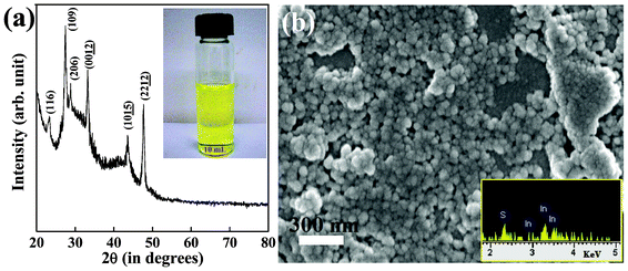 | ||
| Fig. 1 (a) Powder XRD spectrum of In2S3 nanoplatelets. The inset shows the photograph of the stable dispersion of the nanoplatelets in water. (b) SEM image of few layers thick In2S3 nanoplatelets deposited on Cu coated glass substrate. The inset shows a representative EDS spectrum of In2S3 nanoplatelets. The average In:S atomic ratio obtained from the several EDS spectra is 2:2.9, which is near stoichiometric. | ||
Low magnification TEM image of the In2S3 specimen (Fig. 2(a)) revealed that the nanocrystals are almost round, nanoplatelet-like in shape and have nearly monodisperse distribution. The size distribution of the nanoplatelets is represented in a histogram shown in the inset of Fig. 2(a). The average diameter of these nanoplatelets was around 85 nm and conforms to our calculations from the XRD and SEM analyses. A higher resolution TEM image from the zone marked with an orange square is shown in Fig. 2(b). The monodispersity of In2S3 nanoplatelets is clearly visible from the image as well as the size and morphology of the platelets. The platelets have slightly corrugated surfaces with not so sharply defined boundaries. This could possibly be due to the thinness of the nanoplatelets.
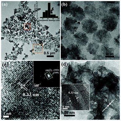 | ||
| Fig. 2 (a) Low magnification TEM image of nearly monodisperse In2S3 nanoplatelets synthesized using 1-thioglycerol as the capping chemical. Inset shows the nanoplatelet diameter histogram. The regions in the figure marked with orange and red squares are shown in (b) and (d), respectively. (b) Higher magnification TEM image showing monodispersity, round shapes and thin nature of In2S3 nanoplatelets. (c) HRTEM image of a single nanoplatelet indicating highly crystalline nature of the structure. A calculated lattice fringe spacing of 0.33 nm indicates (109) plane of tetragonal In2S3. Single crystal SAED pattern shows the reflections from major crystallographic planes of tetragonal In2S3. (d) High resolution TEM image studied from a zone clustered with overlapping In2S3 nanoplatelets (zone marked with red square in (a)) showing some regions where the thin sidewalls are exposed. Inset shows two parallel In2S3 nanoplatelets in upright or tilted positions exposing the thickness (∼7 nm) of the nanoplatelets. Lattice fringe spacing of 0.33 nm is calculated from their thinnest sides. | ||
In order to understand the crystallinity of an individual In2S3 nanoplatelet, lattice fringe pattern and selected area electron diffraction (SAED) pattern were analyzed from a single platelet, which is shown in Fig. 2(c) and in the inset of Fig. 2(c), respectively. Continuous and sharp lattice fringes indicate highly crystalline nature of the platelet and rule out the presence of structural defects in the crystals. A lattice fringe spacing of 0.33 nm matches with the (109) plane of tetragonal In2S3. SAED pattern reveals single crystal structure of the nanoplatelet with clear linear dotted reflections from the planes defined in tetragonal In2S3. Slightly distorted and overlapping diffraction spots in the SAED pattern are contributions from adjacent overlying In2S3 nanoplatelets. Thicknesses of the In2S3 nanoplatelets were then selectively measured from an area where the patterned distributions of the nanoplatelets were destroyed due to clustering (Fig. 2(d), the area marked with red square). The inset of Fig. 2(d) shows the HRTEM image of two upright and/or tilted In2S3 nanoplatelets arranged parallel to each other. As observed from the image, the average thickness of these In2S3 nanoplatelets measured is around 7 nm with a std. deviation of 7–10%. A lattice fringe spacing of 0.33 nm again represented the (109) plane in tetragonal In2S3. The observed monodispersity in size and thickness of In2S3 nanoplatelets may have occurred due to the use of 1-thioglycerol as the capping chemical. In 1-thioglycerol, the presence of strong S–H group at one end and OH group at the other end linked to the C atoms allows shape confinement in In2S3 nanoplatelets by bonding the S end to the platelet surface.51 When 1-thioglycerol was not used to cap the In2S3 nanoplatelets, platelet like shapes still form in In2S3 but larger sizes and broader size distribution makes them polydispersed, as was noticed from Fig. 3(a). In this case, the size range of the platelets without being capped by 1-thioglycerol ranges from 30 nm to 250 nm. SAED pattern collected from clustered In2S3 platelets also shows polycrystalline pattern (inset of Fig. 3(a)) with crystalline diffraction rings visible from major planes in tetragonal In2S3. Higher resolution TEM image (Fig. 3(b)) shows that the thicknesses of the larger platelet structures are ∼10 nm. Fast Fourier transform (FFT) pattern collected from the platelets (inset of Fig. 3(b)) additionally confirms the crystalline nature of the nanoplatelets.
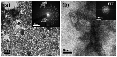 | ||
| Fig. 3 TEM images of the nanostructures formed in a similar chemical environment without using any capping chemical. (a) Clustered polydispersed In2S3 nanoplatelets were observed with the inset showing highly crystalline polycrystalline pattern collected from the nanocrystals. (b) A higher magnification image of the clustered region shows the thinness of the platelets and FFT in the inset confirms polycrystallinity in these structures. | ||
Fig. 4(a) displays the absorption spectrum of In2S3 nanoplatelets in the UV-vis range. A dilute dispersion of the nanoplatelets in water with ∼0.05 absorbance units of optical density at 225 nm was used for collecting the spectrum. A strong absorption peak is observed at 276 nm with a weak shoulder at 365 nm (Fig. 4(a)). This suggests the presence of two energy band positions corresponding to the respective absorption edges in the In2S3 nanoplatelets. The energy gap of bulk In2S3 is ∼2.2 eV with the corresponding absorption edge ∼560 nm.20,27,52,53 As observed from Fig. 4(a), the absorption edge is blue-shifted by almost ∼195 nm compared to the absorption edge in bulk In2S3, which may be related to the strong quantum size confinement in these thin nanoplatelets. With the thickness (7 nm) of the In2S3 nanoplatelets being almost 5 times less than the Bohr diameter of bulk In2S3 (33.8 nm),27,54 quantum confinement in these nanocrystals is expected. The step-like characteristic of the absorption spectrum correlates well with that from the In2S3 nanocrystals prepared by many other researchers using organic capping media and have been explained to be due to valence-conduction band transition in In2S3.27,45,53,55 Room temperature PL spectra for aqueous dispersion of In2S3 nanoplatelets are shown in Fig. 4(b). Unlike bulk undoped In2S3, nano-sized undoped In2S3 are reported to show enhanced luminescence properties.27,53 Using an excitation wavelength of 280 nm, In2S3 nanoplatelets show a strong UV luminescence peak centered around 383 nm, which is only 18 nm Stokes-shifted compared to the absorption peak at 365 nm. The closeness of the absorption and emission peak in In2S3 nanoplatelets is suggestive of the small size dispersion in the specimen. The origin of electronic transitions in emissive In2S3 has remained debatable. While the UV luminescence was related to band-edge emission,53 there are reports that associate it with indirect transitions.20 In many different nano-sized crystals, the emission wavelength maximum was reported to vary with the excitation wavelength because of the size distribution of nanocrystals in a specimen.56 Generally, the shift in the emission peak maximum increases more with the larger crystal size distribution as well as with smaller size of the nanocrystals. We recorded the emission spectra of In2S3 nanoplatelets by varying excitation wavelengths from 220 nm to 320 nm as shown in the inset of Fig. 4(b). As observed from the spectra there are little or no shifts in the emission peak maxima from In2S3 nanoplatelets. This effect may be related to the mono-size dispersion of the diameter (≤5%) of the In2S3 nanoplatelets and contribution from the narrow distribution of thickness (7–10%) of the nanoplatelets in the specimen. A quantum yield of 2% was measured using Horiba JobinYvon QuantumYield calculator from the dispersion of In2S3 nanoplatelets. Currently we are in the process of performing lifetime decay measurements of the luminescence from these In2S3 nanoplatelets that will help us understand more about the transition processes in these thin nanostructures and will be reported elsewhere.
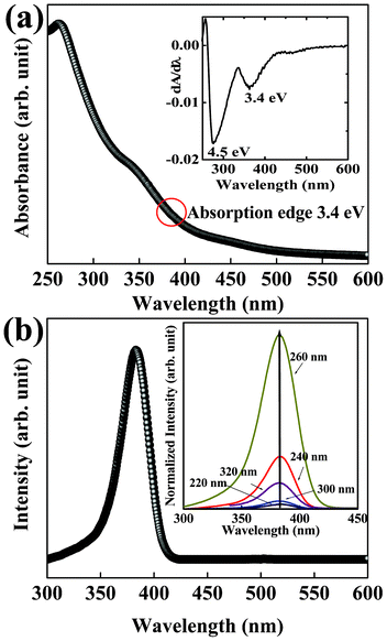 | ||
| Fig. 4 (a) Optical absorbance spectrum collected from the dispersion of In2S3 nanoplatelets shows the presence of step-like pattern. A band gap of 3.4 eV calculated from the lower absorption edge is ∼1.2 eV higher than that reported in the bulk tetragonal In2S3. (b) Room temperature PL spectrum of the In2S3 nanoplatelets shows strong UV emission. As shown in the inset the emission peaks remain unchanged on varying excitation wavelength in the specimen. | ||
Quantum confinement in In2S3 nanoplatelets was also expected to affect the electrical properties of the material. Since In2S3 shows important photoconductance properties in bulk with potential applications in various optical devices including solar cells, we measured the photo I–V properties of our synthesized In2S3 nanoplatelets. Photoconductance (Photo I–V) measurement of the In2S3 nanoplatelets was carried out using a tungsten halogen lamp as the white light solar simulator. Fig. 5(a) shows the schematic configuration of the device fabricated from the In2S3 nanoplatelets. The device was made as discussed in the experimental section and was stable for over a month without any degradation of the material or contacts. Fig. 5(b) shows the I–V characteristic of the hybrid system in the dark and under illumination with the bias ranging from −5 V to 5 V. The I–V curve in the dark exhibited a linear increase from −40 pA to 40 pA resulting in a dark conductivity (σdark) of 3.33 × 10⁻¹⁰ Ω−1 cm−1. As the device was illuminated, the conductance was greatly enhanced and the I–V curve showed a superlinear behavior with a breakdown voltage of ∼4.6 V. Under the highest bias voltage, the current reached above 0.022 μA, resulting in a photoconductivity (σphoto) to a dark conductivity ratio (σphoto/σdark) of more than 102 times.
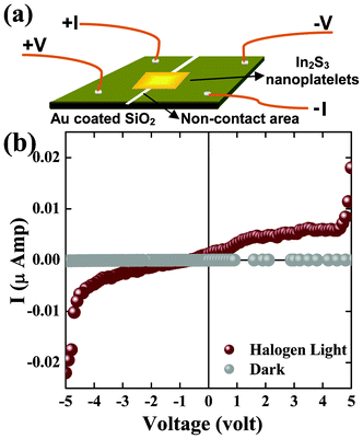 | ||
| Fig. 5 (a) A schematic diagram of the prototype device constructed for measuring I–V of the In2S3 nanoplatelets in light and dark conditions. (b) An I–V graph of the In2S3 nanoplatelets measured in dark and under illumination by a halogen light as the solar simulator. | ||
We know that generally in semiconductor systems, σphoto show linear behavior assuming that neither the mobility nor the lifetime of free carriers in the system is bias dependent.57,58 Previously, we observed non-linear Schottky behavior in In2S3 zigzag nanowires due to contact work function offset.39 The difference between the work functions of In2S3 zigzag nanowires and Au electrodes was responsible for lowering the barrier across the junction and injected electrons from Au-to-In2S3 nanowires.39 However, it is understood that mobility of carriers could also be enhanced under illumination due to barrier height lowering and barrier width narrowing.59–61 In thin nanostructures,62–64 surface adsorption of free ionic species may introduce barriers at the adsorbent sites. The adsorbents upon partial release under illumination lead to an enhancement in the mobility of the carriers. More release of the free ionic species at larger bias may happen due to increase in surface temperature of the nanostructures under longer illumination.63,64 Owing to low thickness of In2S3 nanoplatelets this possibility may not be ruled out. Furthermore, the crystal structure of In2S3 has a considerable number of cation vacancies.24,27 In a vacancy profuse system like In2S3, In atoms may leave their ordered positions and occupy crystallographically ordered vacancies upon excitation (illumination in this case) resulting in an increase in the difference in concentration of ionized donors and acceptors. Consequently, the carrier concentration may increase leading to an enhanced conductivity upon excitation (illumination). The detail mechanism behind the conductivity enhancement in In2S3 nanoplatelets under illumination has yet to be understood, which may furthermore increase the potentiality of our material for direct device applications.
Conclusion
To conclude, we have demonstrated the high yield synthesis of nearly monodisperse In2S3 nanoplatelets of an average of 85 nm diameter and 7 nm uniform thickness by a simple, low temperature, single-step polyol process using ethylene glycol as the solvent medium and 1-thioglycerol effectively as the capping chemical. Without using the capping chemical, nanoplatelet like morphology still formed, but had more polydispersed size and shape. XRD analysis revealed that the nanoplatelets had some selective growth along b-axis and along (116) plane of tetragonal In2S3. Electron microscopy unambiguously confirmed the high crystallinity and uniformity in sizes and shapes of the synthesized nanoplatelets. Optical absorbance revealed large shift in the band gap as compared to the bulk suggesting a strong quantum confinement effect in these thin nanoplatelets. Nearly monodisperse and surface defect free In2S3 nanoplatelets showed steady band edge UV luminescence and almost unchanged PL peak position on varying excitation wavelength. Room temperature photoconductivity measurement performed on a prototype device prepared from the In2S3 nanoplatelets showed an enhancement of more than two orders of magnitude under illumination as compared to that observed in the dark condition. This may be related to the enhancement of mobility of carriers by removal of surface ionic species in these thin nanoplatelets with increasing bias voltage. The present study is intended to open up a new approach in the synthesis of monodisperse In2S3 nanocrystals for efficient optoelectronic applications, such as in solar cells18,19 and as phosphors.20–23Acknowledgements
This work was partially supported by the Florida Cluster for Advanced Smart Sensor Technologies (FCASST) and the United States Army (Grant No. W81XWH1020101/3349).References
- C. B. Murray, C. R. Kagan and M. G. Bawendi, Annu. Rev. Mater. Sci., 2000, 30, 545 CrossRef CAS.
- J. Park, K. An, Y. Hwang, J. G. Park, H. J. I. Noh, J. Y. Kim, J. H. Park, N. M. Hwang and T. Hyeon, Nat. Mater., 2004, 3, 891 CrossRef CAS.
- X. Wang and Y. Li, Chem. Commun., 2007, 2901 RSC.
- J. Park, J. Joo, S. G. Kwon, Y. Jang and T. Hyeon, Angew. Chem., Int. Ed., 2007, 46, 4630 CrossRef CAS.
- A. P. Alivisatos, Science, 1996, 271, 933 CAS.
- X. Peng, J. Wickham and A. P. Alivisatos, J. Am. Chem. Soc., 1998, 120, 5343 CrossRef CAS.
- M. P. Pileni, J. Phys. Chem. B, 2001, 105, 3358 CrossRef CAS.
- A. R. Tao, S. Habas and P. Yang, Small, 2008, 4(3), 310 CrossRef CAS.
- Y. Xia, Y. Xiong, B. Lim and S. E. Skrabalak, Angew. Chem., Int. Ed., 2009, 48(1), 60 CrossRef CAS.
- Y. Jun, J. Seo, S. J. Oh and J. Cheon, Coord. Chem. Rev., 2005, 249, 1766 CrossRef CAS.
- X. G. Peng, L. Manna, W. D. Yang, J. Wickham, E. Scher, A. Kadavanich and A. P. Alivisatos, Nature, 2000, 404, 59 CrossRef CAS.
- D. V. Talapin, N. Gaponik, H. Borchert, A. L. Rogach, M. Haase and H. Weller, J. Phys. Chem. B, 2002, 106, 12659 CrossRef CAS.
- A. I. Ekimov, A. L. Efros and A. A. Onushchenko, Solid State Commun., 1985, 56, 921 CrossRef CAS.
- A. L. Rogach, D. V. Talapin, E. V. Shevchenko, A. Kornowski, M. Haase and H. Weller, Adv. Funct. Mater., 2002, 12, 653 CrossRef CAS.
- W. Shi, R. W. Hughes, S. J. Denholme and D. H. Gregory, CrystEngComm, 2010, 12, 641 RSC.
- C. H. Ho, Y. P. Wang, C. H. Chan, Y. S. Huang and C. H. Li, J. Appl. Phys., 2010, 108, 043518 CrossRef.
- C. H. Ho, J. Mater. Chem., 2011, 21, 10518 RSC.
- N. Naghavi, S. Spiering, M. Powalla, B. Cavana and D. Lincot, Progr. Photovolt.: Res. Appl., 2003, 11, 437 CrossRef CAS.
- J. Sterner, J. Malmstrom and L. Stolt, Progr. Photovolt.: Res. Appl., 2005, 13, 179 CrossRef CAS.
- W. T. Kim and C. D. J. Kim, J. Appl. Phys., 1986, 60, 2631 CrossRef CAS.
- R. Nomura, S. Inazawa, K. Kanaya and H. Matsuda, Appl. Organomet. Chem., 1989, 3, 195 CrossRef CAS.
- T. Asikainen, M. Ritala and M. Leskela, Appl. Surf. Sci., 1994, 82–83, 122 CrossRef.
- E. Dalas and L. Kobotiatis, J. Mater. Sci., 1993, 28, 5456 CrossRef CAS.
- J. Herrero and J. J. Ortega, Sol. Energy Mater., 1988, 17, 357 CrossRef CAS.
- S. Avivi (Levi), O. Palchik, V. Palchik, M. A. Slifkin, A. M. Weiss and A. Gedanken, Chem. Mater, 2001, 13, 2195 CrossRef.
- R. Diehl and R. Nitsche, J. Cryst. Growth, 1975, 28, 306 CrossRef CAS.
- W. Chen, J. O. Bovin, A. G. Joly, S. Wang, F. Su and G. Li, J. Phys. Chem. B, 2004, 108, 11927 CrossRef CAS.
- P. Gao, Y. Xie, S. Chen and M. Zhou, Nanotechnology, 2006, 17, 320 CrossRef CAS.
- Y. Xing, H. Zhang, S. Song, J. Feng, Y. Lei, L. Zhao and M. Li, Chem. Commun., 2008, 1476–1478 RSC.
- Y. H. Kim, J. H. Lee, D. W. Shin, S. M. Park, J. S. Moon, J. G. Nam and J. B. Yoo, Chem. Commun., 2010, 46, 2292 RSC.
- G. Liu, X. Jiao, Z. Qin and D. Chen, Cryst. Eng. Comm., 2011, 13, 182 RSC.
- G. Li and H. Liu, J. Mater. Chem., 2011, 21, 18398 RSC.
- F. Ye, C. Wang, G. Du, X. Chen, Y. Zhong and J. Z. Jiang, J. Mater. Chem., 2011, 21, 17063 RSC.
- L. Liu, H. Liu, H. Kou, Y. Wang, Z. Zhou, M. Ren, M. Ge and X. He, Cryst. Growth Des., 2009, 9, 113 CAS.
- W. Du, J. Zhu, S. Li and X. Qian, Cryst. Growth Des., 2008, 8, 2130 CAS.
- M. A. Franzman and R. L. Brutchey, Chem. Mater., 2009, 21, 1790 CrossRef CAS.
- L. Y. Chen, Z. D. Zhang and W. Z. Wang, J. Phys. Chem. C, 2008, 112, 4117 CAS.
- S. Rengaraj, S. Venkataraj, C. Tai, Y. Kim, E. Repo and M. Sillanpää, Langmuir, 2011, 27, 5534 CrossRef CAS.
- A. Datta, G. Sinha, S. K. Panda and A. Patra, Cryst. Growth Des., 2009, 9, 427 CAS.
- A. Datta, D. Ganguli and S. Chaudhuri, J. Mater. Res., 2008, 23, 917 CrossRef CAS.
- A. Datta, S. K. Panda, S. Gorai, D. Ganguli and S. Chaudhuri, Mater. Res. Bull., 2008, 43, 983 CrossRef CAS.
- A. Datta, S. K. Panda, D. Ganguli, P. Mishra and S. Chaudhuri, Cryst. Growth Des., 2007, 7, 163 CAS.
- A. Datta, S. Gorai, D. Ganguli and S. Chaudhuri, Mater. Chem. Phys., 2007, 102, 195 CrossRef CAS.
- J. Tang, G. Konstantatos, S. Hinds, S. Myrskog, A. G. Pattantyus-Abraham, J. Clifford and E. H. Sargent, ACS Nano, 2009, 3, 331 CrossRef CAS.
- K. H. Park, K. Jang and S. U. Son, Angew. Chem., Int. Ed., 2006, 45, 4608 CrossRef CAS.
- R. H. Bube and W. H. McCarroll, J. Phys. Chem. Solids, 1959, 10, 333 CrossRef CAS.
- Y. Yasaki, N. Sonoyama and T. Sakata, J. Electroanal. Chem., 1999, 469, 116 CrossRef CAS.
- Y. P. Wang, C. H. Ho and Y. S. Huang, J. Phys. D: Appl. Phys., 2010, 43, 415301 CrossRef.
- R. Jayakrishnan, T. Sebastian, T. T. John, C. S. Kartha and K. P. Vijayakumar, J. Appl. Phys., 2007, 102, 043109 CrossRef.
- M. R. R. Menon, M. V. Maheshkumar, K. Sreekumar, C. S. Kartha and K. P. Vijayakumar, Phys. Status Solidi A, 2012, 209, 199 CrossRef CAS.
- N. V. Hullavarada and S. S. Hullavarad, J. Vac. Sci. Technol. A, 2008, 26, 1050 Search PubMed.
- K. Hara, K. Sayama and H. Arakawa, Sol. Energy Mater. Sol. Cells, 2000, 62, 441 CrossRef CAS.
- D. K. Nagesha, X. Liang, A. A. Mamedov, G. Gainer, M. A. Eastman, M. Giersig, J. J. Song, T. Ni and N. A. Kotov, J. Phys. Chem. B, 2001, 105, 7490 CrossRef CAS.
- A. A. Lavrent¢ev, N. Y. Safontseva, V. A. Dubeiko, B. V. Gabriel¢yan and I. Y. Nikifoirov, Phys. Solid State, 2000, 42(11), 2047 CrossRef.
- Y. Nosaka, N. Ohta and H. Miyama, J. Phys. Chem., 1990, 94, 3752 CrossRef CAS.
- W. Hoheisel, V. L. Colvin, C. S. Johnson and A. P. Alivisatos, J. Chem. Phys., 1994, 101, 8455 CrossRef CAS.
- Q. H. Li, T. Gao and T. H. Wang, Appl. Phys. Lett., 2005, 86, 193109 CrossRef.
- D. P. Amalnerkar, Mater. Chem. Phys., 1999, 60, 1 CrossRef CAS.
- H. Kind, H. Yan, B. Messer, M. Law and P. Yang, Adv. Mater., 2002, 14, 158 CrossRef CAS.
- M. T. S. Nair, P. K. Nair and J. Campos, Thin Solid Films, 1988, 161, 21 CrossRef CAS.
- C. H. Wu and R. H. Bube, J. Appl. Phys., 1974, 45, 648 CrossRef CAS.
- D. J. Peña, J. K. N. Mbindyo, A. J. Carado, T. E. Mallouk, C. D. Keating, B. Razavi and T. S. Mayer, J. Phys. Chem. B, 2002, 106, 7458 CrossRef.
- S. E. Ahn, H. J. Ji, K. Kim, G. T. Kim, C. H. Bae, S. M. Park, Y. K. Kim and J. S. Ha, Appl. Phys. Lett., 2007, 90, 153106 CrossRef.
- T. Gao, Q. H. Li and T. H. Wang, Appl. Phys. Lett., 2005, 86, 173105 CrossRef.
| This journal is © The Royal Society of Chemistry 2013 |