Photonic resonant microcavities for chemical and biochemical sensing
Vittorio M. N.
Passaro
*,
Benedetto
Troia
,
Mario La
Notte
and
Francesco De
Leonardis
Dipartimento di Elettrotecnica ed Elettronica, Politecnico di Bari, Via Orabona no. 4, Bari, Italy. E-mail: passaro@deemail.poliba.it; Web: http://dee.poliba.it/photonicsgroup Fax: +39 0805963410; Tel: +39 0805963850
First published on 22nd October 2012
Abstract
Nowadays, photonic sensors represent an efficient and intriguing solution for advanced chemical and biochemical sensing in liquid and gas. In this article, a detailed investigation of photonic sensors based on resonant microcavities is presented. Photonic device architectures, optical sensing principles, technologies and materials are presented, emphasizing their role in optical sensing mechanisms. In conclusion, interesting experimental results are reviewed in order to show the main applications of photonic resonant microcavities in several fields, such as medicine, chemistry and biotechnology, to name a few.
 Vittorio M. N. Passaro | Prof. Passaro received his Laurea degree cum laude in electronic engineering from University of Bari, Italy, in 1988, and his Ph.D. degree from Politecnico di Bari in 1992. In October 2000, he joined Politecnico di Bari as an Associate Professor of Electronic Technologies and Photonics. Since 1988, his research interests have been focused on several theoretical and experimental aspects of optoelectronic and nanophotonic technologies, with more than 270 papers published in refereed international journals and conference proceedings, and over 1000 cites in specialized literature. He is coauthor of two international patents and the editor of three books. |
 Benedetto Troia | Benedetto Troìa was born in Bari, Italy, in May 1985. He received his Laurea Degree (cum laude) in electronic engineering in 2011 from Politecnico di Bari, Italy. In 2011 he received a fellowship from the National Consortium of Telecommunications (CNIT) and his research on advanced silicon photonic sensors based on the Vernier effect was recognized as the best of year 2011. Currently, he is a Ph.D. student in electrical and information engineering. He is coauthor of some papers in conference proceedings and international journals. |
 Mario La Notte | Mario La Notte was born in Trani, Italy, in August 1987. He received his Laurea Degree (cum laude) in Electronic Engineering in April 2012 from Politecnico di Bari, Italy. He joined the Photonics Research Group on January 2012 and his main research interests involve Silicon On Insulator technology, and photonic and optoelectronic integrated circuits for sensing and telecommunications. He is coauthor of some papers published in international journals. |
 Francesco De Leonardis | Francesco De Leonardis was born in Taranto, Italy, in October 1971. He received his Laurea degree in Electronic Engineering in 1999 and his Ph.D. in Electronic Engineering in 2003, both from Politecnico di Bari, Italy. In 2004 he joined Politecnico di Bari as a researcher in electronic engineering. His main research interests are in the fields of non-linear photonic devices, silicon photonics and integrated optical sensors. He is author or co-author of more than 100 papers in international journals and conference presentations, and one international patent. |
Introduction
In recent years, bio/chemical photonic sensors have seen a massive development because of the increasing demand of sensing applications in healthcare, defence, security, environment and food quality control. Moreover, the development and integration of Microfluidic and Photonic technologies, particularly the CMOS-compatible silicon-on-insulator (SOI) technology, allow sensing performance to be significantly enhanced in terms of sensitivity, limit-of-detection (LOD) and detection multiplexing capability. Photonic sensors have been the subject of intensive research, especially for detection of a wide variety of biological and chemical agents. In this context, photonic lab-on-a-chip systems, based on chemical and biochemical sensors, represent state-of-the-art of photonic sensing, since they are expected to exhibit higher sensitivity and selectivity, as well as high stability, immunity to electromagnetic interference, smaller integration sizes and lower costs. Rapid advancements in photonic technologies have significantly enhanced the sensing performance, particularly in the areas of light–analyte interaction, device miniaturization and multiplexing, fluidic design and integration. This has led to drastic improvements in sensor sensitivity, enhanced limit of detection, advanced fluidic handling capability, lower sample consumption, faster detection time and lower overall detection cost per measurement.In this work, we review photonic resonant microcavities designed for chemical and biochemical sensing. In particular, in the first section, basic operation principles of resonant microcavities are briefly introduced. Consequently, conventional optical sensing principles widely employed in chemical and biochemical sensing (e.g., homogeneous sensing, surface sensing, fluorescence, optical absorption, surface Plasmon resonance (SPR), non-linear effects, such as surface enhanced Raman scattering (SERS) and Raman amplification), are reviewed. Afterwards, specific attention is focused on different waveguide structures, materials and technologies employed for the fabrication of planar ring resonator biosensors. In this context, the main design criteria are highlighted, with the aim to improve the sensing performance.
In conclusion, advanced architectures based on resonant microcavities (e.g., liquid core optical ring resonator (LCORR), microsphere and microtoroid microcavities) are investigated, focusing on their sensing performances and future developments.
Fundamental principles of resonant microcavities
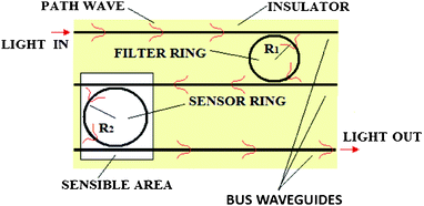
Chemical and biochemical photonic sensors are generally based on the fundamental principle of light–analyte interaction. The aim is to convert the presence of chemical or biochemical analytes into an analytical and measurable optical signal. In conventional photonic sensors based on linear waveguides, the interaction length corresponds to the physical length of the sensor.1,2 Consequently, it is intuitive to suppose that one of the simplest design strategies for improving sensing performance consists of maximizing the interaction length in order to improve the overlap between the propagating optical signal and analytes to be detected, properly concentrated into the sensor sensible area. Generally, this approach yields to the design and fabrication of millimetre-long devices characterized by high performance, but also by high propagation losses suffered over long waveguide paths. However, this result is in contrast with the general trend of realizing ultra-compact lab-on-a-chip characterized by overall footprints as small as ∼mm2. To this purpose, several solutions have been proposed, such as the fabrication of spiral path waveguides and folded photonic devices, able to concentrate mm-long waveguides in compact areas as small as ∼μm2.3Photonic sensors based on resonant microcavities present a number of interesting advantages with respect to conventional photonic sensors. In particular, a traditional planar ring resonator can be sketched, as in Fig. 1. A basic ring resonator architecture is generally represented by two optical bus waveguides, providing input and output ports of the device and properly coupled to the ring architecture.
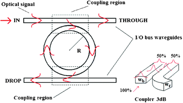 | ||
| Fig. 1 The top view schematic representation of a ring resonator sensor architecture with two bus waveguides. The coupling region is a directional coupler where the input optical signal propagating in the bus waveguide is evanescently coupled to the ring waveguide. The amount of coupled optical power depends on the coupling coefficient r. In the example proposed r = 50%. | ||
When the round-trip phase shift of the ring waveguide is equal to multiples of 2π, circulating lights of different cycles in the ring architecture constructively interfere with each other, resulting in resonance modes at corresponding resonance wavelengths. Moreover, resonance wavelengths can be estimated using eqn (1) below.
 | (1) |
In particular, R is the ring resonator radius, neff is the effective refractive index (RI) of the optical mode propagating in the resonant architecture and m is an integer number (i.e., m = 1, 2, 3,…, n) representing the resonant order.
In Fig. 2, the resonance spectrum at the drop port has been calculated for a ring resonator architecture characterized by a ring radius R ≈ 16 μm and a propagating optical mode with the effective index neff = 2.25.
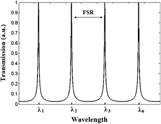 | ||
| Fig. 2 The resonance spectrum at the drop port of the ring resonator. | ||
According to Fig. 2, it is evident that only resonance wavelengths (i.e., λ1, λ2, λ3, λn) periodically spaced by the free spectral range (FSR) can be trapped into the ring and coupled out to the output bus waveguide (i.e., drop port). This mechanism allows us to execute an optical wavelength interrogation in addition to the conventional intensity one at the sensor readout. In fact, it is possible to monitor not only the optical power at the sensor output, but also the corresponding wavelength, using optical spectrum analyzers (OSA) characterized by a typical wavelength resolution equal to ROSA = 80 pm or less.
One of the most important parameter characterizing ring resonators is the quality factor (Q-factor). This parameter represents the number of round trips that circulating resonant optical mode can make in the ring resonator. In aqueous solution, the Q-factor assumes values ranging from ∼104 for planar ring resonators to ∼106 in the case of liquid core optical ring resonators (LCORR).4 In eqn (2), the analytical expression for the calculation of the Q-factor is reported.5
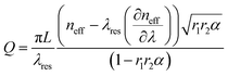 | (2) |
In particular, L is the round trip length in the ring (≈2πR), neff is the effective refractive index valuated at the resonance wavelength λres, α is the optical amplitude attenuation factor due to loss in a single round trip in the ring resonator, r1 and r2 are the optical amplitude attenuation factors that take into account the optical coupling occurring in coupling regions (see Fig. 1), and (∂neff/∂λ) is the derivative of the effective index with respect to the wavelength at the resonant peak, resulting in the definition of the group index ng = neff − (∂neff/∂λ).
Photonic devices based on resonant microcavities are characterized by an effective interaction length Leff, longer than the physical one (i.e., the ring circumference). In particular, the analytical expression for Leff is reported in eqn (3), where all parameters have been already defined.6
 | (3) |
For example, by considering a Q-factor of ∼104 and the resonance near infrared (near-IR) wavelength λ = 1.55 μm, the effective interaction length is estimated to be ∼2.5 mm, much larger than the physical length initially set to 100 μm.
In summary, the capability of resonant microcavities of producing an effective interaction length longer than the physical one, makes these devices very suitable for chemical and biochemical sensing applications. In fact, it is possible to fabricate sensor chips characterized by small footprints with enhanced sensing performance. Moreover, photonic sensors based on resonant microcavities exhibit multiplexing capability and allow us to minimize the amount of chemical species to be concentrated onto the device sensible area.
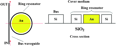
Several ring resonator architectures, such as planar ring resonators, LCORRs, microspheres, microdisks and microtoroids, have been widely investigated in the last few years, exhibiting intriguing sensing performance for chemical and biochemical detection.6 In particular, a schematic illustration of a standard photonic sensor architecture based on planar resonant microcavities is sketched in Fig. 3. The overall sensor is covered by an insulating layer (e.g., silicon dioxide, Teflon, SU-8), being only the ring resonator (i.e., the region in which the greatest percentage of the optical energy is concentrated) directly exposed to the cover medium. Consequently, the sensible area is realized by properly windowing the insulating layer on the resonant microcavity. As it will be well-described in the following, this technological approach is typically employed in the design of advanced lab-on-a-chip devices based on the integration of photonics and microfluidics.
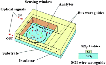 | ||
| Fig. 3 A schematic illustration of a biochemical planar ring resonator-based sensor. The technological platform selected is Silicon on Insulator (SOI). Consequently, buses and ring resonator are supposed to be SOI wire waveguides covered by insulator (SiO2) or exposed to the liquid sample in the sensible area. | ||
Optical sensing principles
Several optical properties can be employed in chemical-to-optical transduction mechanisms for sensing purposes. In particular, it is convenient to distinguish between RI-based sensors and non-RI based sensors, including those based on fluorescence, SERS, SPR and optical absorption.RI sensors based on resonant microcavities
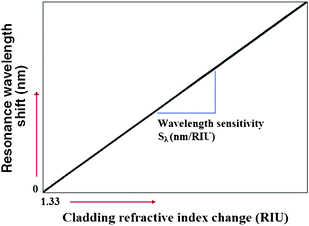
In case of RI-based sensors, two main sensing principles, i.e., homogeneous and surface, can be employed for chemical and biochemical detection.7 In particular, homogeneous (Sh) and surface (Ss) sensitivities are defined as follows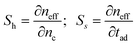 | (4) |
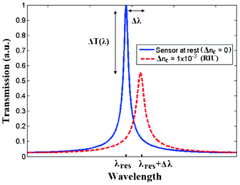
In homogeneous sensing, the modal effective index change is produced by a change of the cover medium refractive index due to the presence of chemical analytes concentrated in the sensing window. In surface sensing, the selective analyte adsorption induces a thickness change Δtad, typically ranging from 1 nm to 10 nm. This thickness change is optically transduced in the modal effective index change, as indicated in eqn (4). Referring to photonic sensors based on resonant microcavities, both homogenous and surface sensing can be used and appreciated by monitoring the wavelength shift characterizing resonance peaks of the ring resonator spectrum, as reported in Fig. 4.
 | ||
| Fig. 4 Optical wavelength readout in RI-based photonic sensors. | ||
By assuming the sensor initially exposed to pure water solution (i.e., sensor at rest) characterized by the refractive index nwater = 1.33, a resonance peak of the ring resonator spectrum characterized by the well-known Lorentzian line-shape is located at the resonance wavelength λres. When biochemical analytes are dissolved in aqueous solution, a cladding refractive index change Δnc occurs, resulting in a detectable resonance wavelength shift Δλ. To this purpose, the assumption of considering a cladding refractive index change Δnc = 1 × 10⁻³ RIU (refractive index unit) is typical for bulk refractive index changes induced by several biochemical analytes.
For example, at 20 °C the refractive index of an aqueous solution of sodium chloride (NaCl) varies with 0.0018 RIU per mass%.8 Moreover, at 20 °C the refractive index of glycerine–water solution varies with ∼1.3 × 10⁻³ RIU per 5% glycerine weight in water.9 However, depending on the chemical/biochemical species to be detected, it could be convenient to design advanced photonic sensors able to detect refractive index changes as low as 10−6–10−7 RIU. For example, the polydimethylsiloxane (PDMS) refractive index change upon xylene is estimated to be dnPDMS/dCxylene = 8.7 × 10⁻⁷ RIU/ppm and the mesoporous silica (MS) RI change upon lead Pb(II) is dnMS/dCPb(II) = 1 ÷ 5 × 10⁻⁶ RIU/ppb, being Cxylene and CPb(II) xylene and lead Pb(II) concentrations, respectively.10
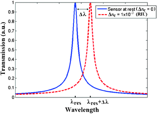
A linear characteristic defines the dynamic range of conventional photonic sensors based on resonant microcavities. In Fig. 5, it is possible to appreciate the linear trend characterizing the resonant wavelength shift as a function of the cladding refractive index change, Δnc.
 | ||
| Fig. 5 Resonance wavelength shift versus bulk RI change in water solution. | ||
In particular, when the sensor works at rest, the resonance peak is located at the resonance wavelength λres, resulting in an overall wavelength shift Δλ = 0 nm.
In this context, homogeneous sensitivity is a performance parameter characterizing the photonic waveguide selected for the sensor design and fabrication. In this sense, by considering the new variable SW, indicating the general waveguide sensitivity, it is possible to define the overall wavelength sensitivity Sλ as the slope of the linear function plotted in Fig. 5. This parameter characterizes a photonic sensor based on single resonance microcavity, as sketched in Fig. 3. In particular, the resonant wavelength shift, the wavelength sensitivity Sλ and the sensor LOD (i.e., the minimum detectable refractive index change) can be defined as follows:11,12
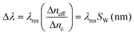 | (5) |
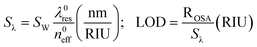 | (6) |
In eqn (5) and (6), λres0 and neff0 are the resonance wavelength and the effective index in unperturbed condition (i.e., only water solution covers the sensor surface), respectively.
In conclusion, Zhu et al. have presented a useful analysis for converting bulk RI sensitivity to biomolecule sensitivity.13 The analysis, generally applicable to all resonant-based RI sensors, leads to the following expression:
 | (7) |
In the case of surface sensing, the wavelength interrogation is performed analogously as already shown for homogeneous sensing. However, detectable resonance wavelength shifts induced by the selective adsorption of target molecules onto the functionalized sensor surface do not originate a linear characteristic, as previously shown in the case of homogeneous sensing (see Fig. 5). In fact, the typical sensor characteristic generated in the case of surface sensing is characterized by the well-known Langmuir's curve path, as plotted in Fig. 6.14,15
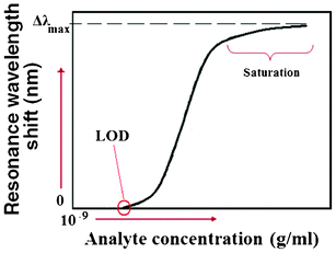 | ||
| Fig. 6 Resonance wavelength shift versus different analyte concentrations in the case of surface sensing. | ||
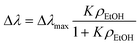
In this context, Yebo et al. have estimated a resonance wavelength shift of 200 pm corresponding to the adsorption of 120 ppm of ethanol (EtOH), assuming the resonance wavelength shift Δλ is proportional to the volume of adsorbed ethanol, according to eqn (8):15
 | (8) |
In the Langmuir model equation reported above, K is an equilibrium constant, Δλmax is the maximum wavelength shift and ρEtOH is the partial pressure of ethanol equal to cEtOH/106 bar, cEtOH being the ethanol concentration.
In the case of surface sensing, it is convenient to refer to the so-called refractive index increments, usually indicated as dn/dc. This parameter allows us to linearly correlate optical properties (i.e., refractive index n) of a particular chemical analyte (e.g., protein) to its concentration c, in a wide range of concentrations.16 For example, the refractive index increase of streptadivin is estimated to be 0.212 ml g−1.17
Consequently, by knowing the refractive index increment of the chemical species to be detected, the absolute amount of the absorbed molecules over the functionalized sensor surface can be estimated by using de Feijter's formula as follows:18,19
 | (9) |
In eqn (9), Γ is the molar surface coverage, na is the refractive index of the adsorbed molecules, nc is the cover medium RI. Consequently, the mass density ρ of the molecular adlayer adsorbed on the sensor surface can be estimated for biological analytes whose molecular weight M is known, since molar surface coverage can be also expressed as follows:19
 | (10) |
Referring to photonic sensors based on resonant microcavities, the minimal detectable protein mass ΔMmin can be estimated as:
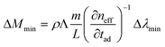 | (11) |
Non-RI sensors based on resonant microcavities
In non-RI-based photonic sensors the modal effective index is not used in the chemical-optical transduction process. In fact, other optical properties, such as optical absorption, fluorescence, SPR and SERS, can be employed, taking advantage of enhanced light–matter interaction distance and enhanced optical field near the photonic sensor surface for better sensing performance.Optical absorption is mathematically defined by the Beer–Lambert law, as in eqn (12) below:
| I = I0exp(−αL), α = εC | (12) |
In particular, I is the light intensity at the end section of the overall sensor path length L and I0 is the light intensity at the initial section of the sensor sensible area. The absorption coefficient α linearly depends on the analyte concentration C and on its molar absorption coefficient ε.20,21 Consequently, by measuring the ratio I/I0 with a power meter, it is possible to estimate the analyte concentration in the sensible area. Optical absorption has been widely employed in optical spectroscopy because a lot of gases and liquids are characterized by high absorption coefficients in near and mid-infrared (mid-IR). For example, mid-IR absorption strength of methane (CH4) is 160 times larger than that estimated in near-IR. In addition, formaldehyde, water, ammonia and carbon dioxide, are characterized by absorption coefficients α (cm−1) ranging from a few tens to 60 cm−1 in near mid-IR (i.e., 2–8μm).20
To this purpose, an integrated photonic sensor based on the Vernier effect and employing both homogeneous sensing and optical absorption, has been recently designed and theoretically simulated for methane and ethane detection in mid-IR.22 Interesting performances have been achieved. In fact, sensitivities as high as 224.4 μm RIU−1 and 218.51 μm RIU−1 have been theoretically demonstrated for methane and ethane detection, respectively. Moreover, LODs as low as ∼2 × 10⁻⁵ RIU enable the detection of a minimum percentage of methane and ethane in air volume, equal to 2% and 1%, respectively.
In general, resonant microcavities simultaneously employing homogeneous sensing and optical absorption allow a multiple intensity and wavelength interrogation to be achieved. To this purpose, in Fig. 7 a schematic of a spectral response characterizing a planar resonant microcavity employing both effects mentioned above, is sketched.
 | ||
| Fig. 7 Spectral response of a resonant microcavity sensor employing both homogeneous sensing and optical absorption. | ||
According to Fig. 7, the homogeneous sensing induces a wavelength shift Δλ proportional to the cover refractive index change Δnc. Moreover, the effect of the optical absorption causes transmission intensity changes ΔT(λ), depending on the absorption spectrum of the analyte to be detected. In this way, the advantage of employing optical absorption mechanism for chemical and biochemical detection consists in the possibility to find the signature of the gas or chemical/biochemical specie to be sensed, significantly improving the sensing performance.
In fluorescence measurements, the target analyte can be a natural chromophore or must be labelled with fluorophores (e.g., dyes).14 In particular, the sensing process consists of detecting the fluorescence intensity signal changes in a precise wavelength range. The use of resonant microcavities allows us to enhance the intensity of the fluorescence signal proportionally to the quality factor Q. Typically, fluorescence-based sensors have been employed for DNA hybridization process monitoring or for gene expression profiling.23,24
In this context, J. T. Kirk et al. have proposed a non-contact piezoelectric (inkjet) method for the rapid and efficient printing of bioactive protein, glycoproteins and neoglycoconjugates onto a high-density silicon microring resonator biosensor array.25 The biosensor consists of an array of 32 microring resonators characterized by a 30 μm long diameter. In particular, 24 ring resonators are exposed for biosensing, while the remaining 8 microcavities are coated with a fluoropolymer cladding for enabling temperature and vibration reference controls. Doubly resonant porous silicon microcavities have been proposed for enhanced detection of fluorescent organic molecules.26 Sensing performances of the proposed structures have been tested by using larger molecules of fluorescein-labelled protein A as target analytes. Authors have demonstrated that small concentrations of fluorescent dyes down to a few picomoles, can be detected.
In conclusion, although interesting performance can be achieved by fluorescent photonic sensors based on resonant microcavities, some constrains limit their mass-scale production. In fact, quantitative analysis of DNA remains challenging due to the fluorescence signal bias, as the number of fluorophores on each DNA target molecule cannot be precisely controlled. In addition, photonic sensors based on fluorescence are not label-free, thus their reliability and measurement reproducibility are not suitable for sensor massive uses and point-of-care testing.
Photonic sensors based on SPR represent the commercial optical solution typically employed for bio/chemical sensing. SPR-based sensors have been demonstrated to be suitable for label-free detection of pico/femto-molar concentrations of biological analytes, such as DNA with LODs as low as 1.4 × 10⁻⁷ RIU,27 RNA, pesticides28 and allergens, to name a few.29 Recently, intriguing investigations have been carried out concerning with potential applications of SPR in early diagnosis and progression of Alzheimer's disease.30 To this purpose, amyloid-β (Aβ) fibril formation and interaction monitored by SPR have been documented.
A surface plasmon is a localized electromagnetic wave that propagates along the metal–dielectric interface and exponentially decays into both media. Surface plasmons can be excited due to the resonant transfer of the incident photon energy and momentum to collectively oscillate in a noble metal. In particular, the surface plasmon dispersion relation at the resonance condition can be written as:
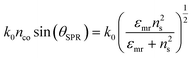 | (13) |
In this context, L. Zhou et al. have theoretically investigated a novel miniature biochemical sensor based on a 1 μm-radius hybrid plasmonic microring resonator in SOI techonology.32 A schematic representation of the sensor configuration is sketched in Fig. 8.
 | ||
| Fig. 8 Top and cross-sectional views of the hybrid plasmonic microring resonator in SOI technology. The surface plasmon waves are concentrated in the slot region inbetween silicon and gold and propagates along the ring resonator. | ||
The excitation of the surface plasmon waves coupled to the dielectric silicon photonic modes, results in a high optical field concentration in the slot region between metal (i.e., gold) and silicon. A sensitivity as high as 580 nm RIU−1 and a LOD of the order of ∼1.5 × 10⁻⁴ RIU have been theoretically estimated, suggesting that this sensor configuration is suitable for label-free biochemical diagnoses. In conclusion, a sensitivity of 1000 nm RIU has also been theoretically demonstrated in a nanoplasmonic ring resonator operating in near-IR.33
In photonic sensors based on SPR, the penetration depth of surface plasmon evanescent field is about 100 nm. Consequently, the detection of large target molecules, such as cells and bacteria, can be difficult to execute. In addition, SPR photonic sensors do not allow us to distinguish between specific and nonspecific interactions, thus between the refractive index surface change and the bulk solution refractive index change. Finally, the instability of nanostructure morphology and optical properties can compromise both reliability and repeatability of measurements.
In conclusion, the sensing principle based on the non-linear surface-enhanced Raman scattering represents an intriguing spectroscopic tool for non-invasive and non-destructive detection of biochemical and chemical molecules. SERS is a surface-sensitive technique able to detect the enhancement in Raman scattering when target molecules are adsorbed onto the metal surface. Several research efforts are still ongoing in this application field. For example, nanocone structures have been fabricated for SERS. In particular, these novel nanostructures support the detection of subtle changes in peptide probe sequences, such as single amino acid phosphorylation or mutation.34 Large area Au nanogap plasmon resonator array substrates have been recently proposed as ideally suited scattering sites for SERS, as well as refractive index sensing.35 The use of SERS in conventional resonant microcavities has been well demonstrated by I. M. White et al.36 In particular, a liquid core optical ring resonator (LCORR) has been employed as a microfluidic channel and as a ring resonator for the excitation of metal nanoclusters and target analytes as they pass through the channel. The lab-on-a-chip proposed has been demonstrated to be able to detect Rhodamine 6G (R6G) in silver colloid, revealing a detection limit as low as 400 pmol L−1 (i.e., the Raman signal generated by only a few hundred of R6G molecules). Although interesting performance can be achieved, the integration of resonant microcavities based on SERS effect onto a compact and CMOS-compatible technological platform still remains challenging.
For these reasons, Raman effect and amplification have been properly investigated in integrated SOI microcavities, such as microdisk and racetrack resonators.37 Moreover, a cascade Raman laser based on SOI optical waveguides and coupled resonant microcavity and operating in the midwave infrared region has been proposed for ethane (C2H6) and carbon dioxide (CO2) detection.38
Optical waveguide structures and materials employed in photonic planar ring resonators
Photonic sensors based on planar resonant microcavities can be realized using several waveguide architectures that have been properly designed and optimized for sensing applications. In particular, it is convenient to distinguish between the well-known rib, wire and slot optical waveguides for understanding the importance of the waveguide architecture on the overall resonant microcavity-based sensor design and performance.Referring to the standard SOI technology, all waveguides shown in Fig. 9 are characterized by sub-micrometer dimensions. In fact, a slot waveguide in SOI technology (see Fig. 1c) designed and optimized for homogeneous sensing in aqueous solution at the operative wavelength λ = 1.55 μm is characterized by silicon photonic wire height and width of 324 nm and 180 nm, respectively, while the gap region separating two symmetrical silicon wires is 100 nm large.39 Similar dimensions characterize rib and silicon-wire waveguides, too. In fact, SOI technology allows a very high refractive index contrast between silicon and its oxide (e.g., nSi ≈ 3.45, nSiO2 ≈ 1.45, thus Δn ≈ 2 @ 1.55 μm). Consequently, by using SOI technology it is possible to confine the optical signal in very small, single-mode guided-wave architectures, enabling the fabrication of ultra-compact sensor chips. Optical losses can represent a technological constrain in the design and fabrication of integrated photonic sensors based on resonant microcavities. However, relevant improvements in technological facilities and processes result in the capability of fabricating ultra-low loss SOI waveguides. For example, silicon photonic wire waveguides with a cross-section of 450 nm × 220 nm have been fabricated, exhibiting propagation losses of 0.8 dB mm−1 for quasi-TE optical mode (the electric field of which is parallel to the substrate) and 0.6 dB mm−1 for quasi-TM mode (electric field perpendicular to the substrate).40 Compact and low loss sub-micrometer SOI rib waveguides have been fabricated and characterized, revealing propagation losses as low as ∼0.5 dB cm−1.41 Finally, slot waveguides fabricated in SOI technology ensure ultra high performance in homogeneous and surface sensing, but their propagation losses still remain high enough (e.g., ∼1.3 ± 0.2 dB mm−1, ∼11.1 ± 1.15 dB cm−1 at λ = 1.55 μm).42,43
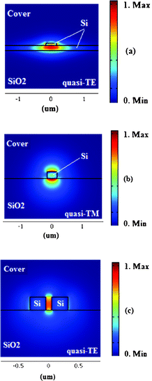 | ||
| Fig. 9 Waveguide architectures: (a) rib, (b) wire and (c) slot. | ||
In order to enhance the optical sensing response (i.e., the effective index change Δneff in the case of homogeneous or surface sensing), it is obviously necessary to maximize the overlap between the propagating optical field and the analytes concentrated in cover medium. In particular, in photonic wire waveguides the evanescent field exponentially decays as a function of δ, i.e., the penetration depth.44 This parameter depends on the difference between the mode effective index and the index of refraction of the cladding layer, as in eqn (14):
 | (14) |
In this way, SOI technology represents an efficient solution for ensuring the optical signal localization near the sensor surface. In fact, it is evident that the greater the difference between neff and nc the smaller the penetration depth. In silicon wire waveguides, the high refractive index core ensures a very high optical field confinement near the sensor surface where target molecules are selectively adsorbed (i.e., surface sensing), or simply concentrated, producing changes in the cladding material optical properties (i.e., homogeneous sensing).
In Fig. 10, a folded cavity ring resonator sensor based on silicon photonic wire waveguide is sketched.45 The folded spiral path geometry represents a feasible and efficient solution for enhancing sensor interactions lengths. In fact, in the photonic sensor proposed the folded cavity allows us to enclose a 1.2 mm long ring waveguide (i.e., quality factor Q = 19,600), in a 150 μm diameter sensor area.
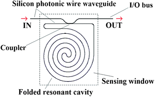 | ||
| Fig. 10 A planar ring resonator based on silicon photonic wire waveguide characterized by a folded cavity geometry. | ||
In this way, a folded millimetre interaction length allows us to further improve the overall overlap between the propagating optical field and the chemical species to be detected, properly concentrated near the sensor surface (i.e., light-analyte interaction). Moreover, small cavity dimensions require less analyte for full coverage of the sensor surface. The sensor chip is covered by SU-8 polymer with the only exception of the sensing window opened over the sensible area, thus over the folded cavity geometry, as shown in Fig. 10. The functionalized spiral cavity sensor surface has been exposed to streptavidin for monitoring the stable streptavidin/biotin protein binding. Sensor performance exhibits a LOD as low as ∼3 pg mm−2 (i.e., a total mass of ∼5 fg).
Although rib waveguides allow to obtain very low propagation losses, they do not allow us to maximize the field confinement factor in te cover medium, in particular near the sensor surface. In fact, in Fig. 9a it is possible to appreciate how the optical field distribution is significantly confined in the high refractive index silicon core. To this purpose, a SOI rib waveguide optimized for homogeneous sensing in aqueous environment (i.e., cover refractive index ranging from nc ∼1.33 (water) to 1.5 (protein)), exhibits an homogeneous sensitivity of 1.8 × 10⁻³ in the telecommunication wavelength range 1.3–1.5 μm.46 A rib silicon nitride (Si3N4) waveguide structure on silicon oxide SiO2 buffer layer has been optimized for surface sensing by simulating the biochemical ad-layer adsorption on the functionalized sensor surface, with its thickness ranging from 2 nm to 4.8 nm. Theoretical results have demonstrated a surface sensitivity Ss ∼2 × 10⁻⁴ nm−1 around 1.55 μm.47 On the contrary, a silicon photonic wire waveguide based on SOI technology, designed and optimized for homogeneous sensing in water environment (nc ∼ 1.32) at λ = 1.55 μm, is characterized by a sensitivity Sh = 0.31.48 In addition, a silicon photonic wire waveguide with silicon core thickness of 220 nm, exhibits a surface sensitivity Ss = 4.42 × 10⁻³ nm−1 by assuming an ad-layer with refractive index 1.5 and thickness of 2 nm for an input wavelength of λ = 1550 nm.44 These results evidence that silicon photonic wire sensitivity is two orders of magnitude larger than in rib waveguides, and two to five times larger compared to optimized photonic wire waveguides made of silicon nitride (Si3N4).48
In conclusion, slot waveguides have been widely used and demonstrated in photonic sensing because of their capability to confine a great percentage of the propagating optical field in the low index region, in particular into the slot region (see Fig. 9c). In fact, according to eqn (15), the higher the refractive index contrast between high and low refractive index regions, indicated by nH and nL respectively, the higher the electromagnetic field (E-field) in the low refractive index region.20
 | (15) |
In eqn (15), EL is the component of the E-field evaluated in the low refractive index region and EH is the E-field component in the high refractive index region. Consequently, by considering SOI technology (Δn ∼2 @ 1.55μm), interesting performance have been theoretically and experimentally demonstrated for sensing applications.20,49 In fact, SOI slot waveguides optimized for homogeneous sensing in a water environment can exhibit sensitivities higher than unit (i.e., Sh > 1) in near-IR, for quasi-TE E-field polarization.39 A surface sensitivity as high as 4.31 × 10⁻⁴ nm−1 has been theoretically demonstrated for a conventional slot waveguide,39 resulting in surface sensing performance approximately two times larger than that exhibited by SOI photonic wire waveguides.
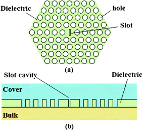
Finally, all numerical results confirm slot waveguides as the highest performance wave-guiding structure for biochemical sensing applications (e.g., detection of acetylene C2H2, NaCl).50 To this purpose, an asymmetric Si3N4 slot-waveguide (w2 = 550 nm, w1 = 400 nm) on a SiO2 buffer layer has been integrated in a 70 μm radius microring resonator, as sketched in Fig. 11.51 Asymmetric slot waveguides are 300 nm thick and the slot region gap is 200 nm, facilitating a complete slot filling by liquid solution.
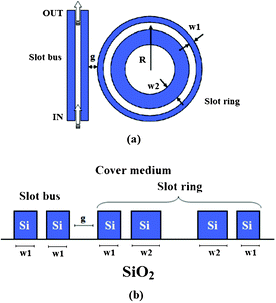 | ||
| Fig. 11 The top view of a ring resonator based on asymmetric slot waveguides (a). Cross-section of the slot ring resonator coupled to a single slot bus waveguide, both based on SOI technology (b). | ||
Homogeneous sensing has been simulated and experimentally demonstrated by exposing the sensor chip to water solution, isopropanol and cyclohexane with different concentrations (i.e., different cover medium refractive indices). The resulting homogeneous sensitivity is estimated to be Sh = 212.13 nm RIU−1 with a LOD as low as 2.3 × 10⁻⁴ RIU.52 The same photonic sensor has been experimentally characterized for surface sensing by monitoring the molecular binding events between bovine serum albumin (BSA) and anti-BSA.53 The biosensor exhibits sensitivities of 1.8 and 3.2 nm/(ng × mm−2) for the detection of anti-BSA and BSA, respectively. Moreover, detection limits are 28 and 16 pg mm−2 for anti-BSA and BSA, respectively.
Finally, Claes et al. have designed and fabricated a slot-waveguide-based ring resonator in SOI technology characterized by a footprint of 13 μm × 10 μm.54 Experimental results reveal very high sensing performance. In particular, a homogeneous sensitivity of 298 nm RIU−1 and a LOD as low as 4.2 × 10⁻⁵ RIU have been achieved by exposing the sensor chip to different concentrations of saline solutions (i.e., NaCl in water).
Materials and technology
Nanophotonic waveguides in SOI technology represent an intriguing and efficient solution for the fabrication of ultra compact sensor chips based on resonant microcavities. In addition, low-cost and mass-scale production can be ensured because of the possibility to adapt standard CMOS fabrication processes for fabricating photonic nanostructures.As reported in previous section, photonic devices based on SOI technology are characterized by a high refractive index contrast. Consequently, in order to obtain a single-mode waveguide, its cross-section must be reduced to the order of (λ/ncore)2, λ being the operative wavelength of the light in vacuum and ncore the refractive index of the waveguide core.
A consequence of the high lateral index contrast is that silicon waveguides become more sensitive to scattering due to core-cladding interface roughness.55 However, photonic waveguides characterized by sub-micrometer dimensions can be fabricated with high-quality and high-resolution by using standard CMOS processes, including 193 nm-deep UV lithography, inductively coupled plasma reactive ion etching (ICP-RIE) and chemical vapour deposition (CVD) for silicon photonic waveguide passivation.
The choice of the material system to be employed for design and fabrication of photonic biochemical sensors depends on the sensing application and performance. In fact, as reported in Table 1, the higher the refractive index contrast Δn, the higher the detectable effective index change.
To this purpose, step-index slab waveguides made of different materials (i.e., silicon, Si3N4, polymer and silica) and assumed on a silicon oxide SiO2 buffer layer have been simulated for both homogeneous and surface sensing, in order to calculate effective index changes, indicated with Δneff(H) and Δneff(S), respectively.48
In particular, effective index changes of the TM-polarized optical mode propagating in slab waveguides with core thickness tcore at the operative wavelength λ = 1.55 μm have been calculated in the case of homogeneous sensing by assuming a fixed cover refractive index change of 0.01 RIU. In the case of surface sensing, the presence of a 4 nm thick molecular ad-layer of refractive index 1.5 in a water environment has been assumed. Finally, it is possible to quantitatively evaluate the advantage of the SOI platform in terms of best sensing performance and very small dimensions, according also to numerical results of sensitivities and LODs, as previously reported about ring resonator sensors based on photonic wire and slot waveguides.
Although polymers cannot ensure high refractive index contrast, they have been widely used for photonic sensing applications because of their high biocompatibility and technological feasibility. In particular, an exotic high index contrast polymer waveguide platform has been proposed for integrated biophotonics. Polymethylmethacrylate (PMMA) polymer has been employed for fabricating the waveguide core material on the fluorinated optical polymer Cytop employed as substrate.56 The refractive index contrast between PMMA core waveguide and Cytop polymer is estimated to be approximately 0.15, being nPMMA ∼1.49 and nCytop ∼1.34. The calculated contrast is one order of magnitude larger than in conventional polymer waveguides fabricated in SOI technology (see Table 1). The proposed waveguide has been fabricated and integrated in simple racetrack ring resonators characterized by ring diameters ranging from 20 μm to 60 μm and a nominal coupling gap of 200 nm. Q-factors of the order of ∼104 can be achieved, making these polymer-based sensors suitable for biochemical sensing.
Planar ring resonators based on polymer waveguides have been proposed for biomolecules detection.57 The waveguide cross-section is sketched in Fig. 12.
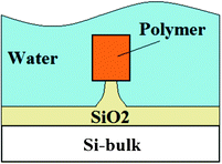 | ||
| Fig. 12 The cross-section of the polymer core waveguide supported by an oxide pedestal structure. | ||
Polymer waveguides, such as that shown in Fig. 12, are difficult to fabricate using conventional fabrication techniques. To this purpose, authors have developed an effective fabrication technique based on nanoimprint lithography. This direct imprinting technique can be employed for the fabrication of several polymer-based waveguides, such as PMMA, polystyrene (PS), polycarbonate and SU-8. Chao et al. have fabricated PS microring resonators based on a waveguide with large dimensions (i.e., height of 1.85 μm and width of 2.3 μm).57 The gap between ring and bus waveguide ranges from 200 nm to 400 nm. These microring devices with a quality factor Q ∼20![[thin space (1/6-em)]](https://www.rsc.org/images/entities/char_2009.gif) 000 exhibit a LOD as low as 10−7 RIU for homogenous sensing of glucose solutions dissolved in deionized (DI) water. In addition, these sensors are able to detect the binding of specific biomolecules (i.e., biotin–BSA, streptavidin–biotin) with a LOD of ∼250 pg mm−2 of mass coverage. Although these sensors reveal ultra-high performance, they are not suitable for mass scale production because of the impossibility of using standard CMOS fabrication processes.
000 exhibit a LOD as low as 10−7 RIU for homogenous sensing of glucose solutions dissolved in deionized (DI) water. In addition, these sensors are able to detect the binding of specific biomolecules (i.e., biotin–BSA, streptavidin–biotin) with a LOD of ∼250 pg mm−2 of mass coverage. Although these sensors reveal ultra-high performance, they are not suitable for mass scale production because of the impossibility of using standard CMOS fabrication processes.
Ring resonators based on SU-8 multiple slot waveguides have been fabricated and experimentally tested for label-free biochemical sensing.58 The cross-section of the proposed waveguide is shown in Fig. 13 below. By using multiple slot waveguides, it is possible to significantly increase the sensitivity in the case of homogeneous and surface sensing.59,60
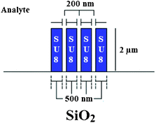 | ||
| Fig. 13 The cross-section of SU-8 multiple slot waveguide.58 | ||
Enhanced sensing performance is achieved because the interaction between the optical field and the chemical test sample can be distributed over a larger area in comparison to a single slot waveguide. The number of slots practically achievable in a multiple slot waveguide depends on technological and optical constraints, such as light coupling mechanisms, scattering losses and single mode operation, but the best choice is usually three. Circular ring resonators with 200 μm circular radius based on SU-8 multiple slot waveguides, as sketched in Fig. 13, have been experimentally tested for both homogeneous and surface sensing. A homogeneous sensitivity Sh = 244 nm RIU−1 has been obtained by exposing the photonic sensor to different mass concentrations of NaCl (0–4%) in DI water. In the case of surface sensing, interesting performances have been achieved for biotin–BSA protein binding events. In fact, SU-8 hydrophobic property allows us to selectively immobilize molecules by physical adsorption onto the functionalized surface, forming a detectable biochemical monolayer. In conclusion, although low refractive indices characterizing several polymers (in the range 1.3–1.8) do not allow us to fabricate ultra-small photonic devices as in SOI technology, polymeric waveguides exhibit low surface roughness scattering and enhance coupling efficiency to optical fibres. Moreover, several polymers can be properly synthesized in order to render specific properties, such as special surface functionalities, optical non-linearity and optical amplification. Finally, polymer refractive indices are generally sensitive to high temperature. To this purpose, although practical sensing applications are performed at room temperature, different solutions have been applied for active temperature control.61 For example, a photonic glucose sensor based on two polymer ring resonators exhibits a measurement error as low as 0.03 (g dL−1) °C−1 by enabling a temperature compensation through a reference polymer ring resonator integrated on the sensor chip.61
Porous materials represent an intriguing alternative to conventional technologies typically employed for photonic biochemical sensor fabrication. In this context, nanoporous silicon is a versatile material attractive for chemical and biochemical sensors because of its very high surface area to volume ratio, simple and inexpensive fabrication techniques and suitability with CMOS technology. Furthermore, by using a porous material it is possible to fabricate label-free photonic sensors with high performance. In particular, the sensitivity can be enhanced because the porous material matrix offers a larger area to be functionalized for selective detection of biomolecules. Thus, a porous silicon microcavity has been fabricated in order to realize a bacteria detection chip for molecular or submolecular analysis by surface modification using undecylenic acid and the specific recognition binding of vancomycin to the D-alanyl-D-alanine of bacteria.62 The sensor proposed exhibits a LOD as low as 20 bacteria ml−1, demonstrating high sensitivity, good reproducibility, fast response and low cost for biosensing. Moreover, Mancuso et al. have proposed and fabricated nanoporous polymer ring resonators for chemical and biochemical detections.63 Racetrack resonators of size ranging from 35 μm radii (and 20 μm coupling lengths) to 65 μm radii (and 30 μm coupling lengths), based on polystyrene nanoporous waveguides combined with polymeric microfluidics, have been tested by exposing the sensor to different glucose concentrations. Experimental results evidence a sensitivity enhancement of 42% of porous resonators compared with nonporous ones. Recently, Yebo et al. have demonstrated selective and reversible ammonia (NH3) gas detection with functionalized SOI optical microring resonators with a 5 μm-long radius.64 By coating the sensor with acidic nano-porous aluminosilicate films, a reversible response to NH3 with selectivity relative to carbon dioxide (CO2) has been experimentally demonstrated, exhibiting a limit of detection as low as 5 ppm. A similar sensor architecture has been also proposed as an ethanol vapour sensor (C2H5), by coating ring resonators with a porous zinc oxide (ZnO) nanoparticle film.15 The porous nature of the coating provides a large surface for gas adsorption. In fact, microring resonance shifts induced by ZnO refractive index change upon vapour adsorption, reveal detectable ethanol vapour as low as 100 ppm and a detection limit estimated to be below 25 ppm.
In conclusion, appropriate alloys of group IV materials have been applied in SOI technology for homogeneous sensing in mid-IR (i.e., at λ = 2.883 μm and λ = 3.39 μm).21,65 In Fig. 14, two examples of group IV materials-based slot waveguides are sketched.
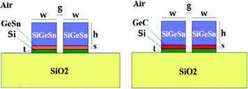 | ||
| Fig. 14 Slot waveguides based on group IV material alloys on SiO2. | ||
Group IV materials are characterized by high refractive indices at mid-IR operative wavelengths. In particular, the Si0.08Ge0.78Sn0.14 alloy is characterized by a refractive index as high as 4.3202 @ 2.883 μm and 4.2960 @ 3.39 μm.21,65 Moreover, Ge0.97C0.03 and Ge0.91Sn0.09 alloys exhibit refractive indexes of around 4 at both mid-IR wavelengths mentioned above too. In this way, high refractive index contrasts allow to obtain ultra-high homogeneous sensitivities, i.e., Sh > 1. The integration of group IV-based slot waveguides in planar resonant microcavities characterized by ring radii of approximately 60 μm has been theoretically investigated revealing high sensing performance for gas detection in mid-IR (e.g., methane (CH4) at 3.39 μm). In fact, LODs as low as 3.64 × 10⁻⁵ RIU and homogeneous sensitivities higher than 2 μm RIU−1 have been theoretically estimated.
In conclusion, fabrication tolerances have been taken into account by considering slot waveguides characterized by non-vertical sidewalls. To this purpose, a tilting angle θ ≠ 0° has been introduced in simulations.
Numerical results plotted in Fig. 15 reveal high fabrication tolerances of group IV-based slot waveguides at both mid-IR operative wavelengths. In fact, homogeneous sensitivities remain higher than 0.9 for tilting angles lower than 4°, which is achievable by a standard ICP-RIE etching process. Similar investigations have been widely discussed about conventional silicon slot waveguides fabricated on SOI wafers.66
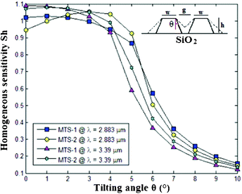 | ||
| Fig. 15 Homogeneous sensitivities of group IV-based slot waveguides as a function of different tilting angles. MTS-1: Ge(0.78)Si(0.08)Sn(0.14)-on-Ge(0.97)C(0.03)-on-Si, (t = 20 nm, w = 390 nm, s = 50 nm, h = 560 nm; MTS-2: Ge(0.78)Si(0.08)Sn(0.14)-on-Ge(0.91)Sn(0.09)-on-Si (t = 20 nm, w = 380 nm, s = 50 nm, h = 520 nm). | ||
Finally, the group IV alloys considered above constitute a new paradigm in the design and fabrication of silicon photonic sensors. However, some technological constraints, such as the impossibility of using standard CMOS processes, and the impossibility of selectively growing these alloys directly on SiO2, still limit their mass-scale production.
Silicon surface chemical functionalization
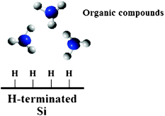
Sensing performance characterizing photonic sensors based on resonant microcavities depend on both optical and chemical prerogatives. In fact, as analysed in the previous section, the choice of both materials, technology and waveguide architectures represents a very important step in the overall photonic sensor design. On the other hand, once the integrated photonic sensor chip is fabricated with respect to specific optical requirements (e.g., operative wavelength, sensing principle, linear or non-linear operative regime, and so on), chemical surface functionalization represents a fundamental aspect for enhancing sensor LOD and selectivity.67Among several nanomaterials and nanotechnologies usually employed for photonic sensing (e.g., molecular imprinted polymers, metal complexes, sol–gel materials, organic ligands, to name a few) it is possible to distinguish between two fundamental preparation strategies for silicon surface functionalization: silanization and hydrosilylation. The former is the chemical process used for covering the silicon surface through self-assembly monolayer with organofunctional alkoxysilane molecules. Generally, surface silanization is applied after silicon surface oxidation because SiO2 contain hydroxyl groups, which attack and displace the alkoxy groups of silane, forming a covalent –Si–O–Si– bond. The SiO2 layer located on the silicon surface can be a thin native oxide film with a thickness of 1–2 nm, or it can be a thermally grown oxide passivation layer with thicknesses ranging from 10 nm to 20 nm.
In this context, silicon photonic microring resonators have been proposed for quantitative cytokine detection and T-cell secretion analysis. In particular, the microring resonator sensing platform is used to detect the 15.5 kDa human cytokine interleukin-2 (IL-2) at concentrations down to 100 pg mL−1 (6.5 pM).68 Sub-ng mL−1 sensitivity and ultra-low LOD have been achieved by properly functionalizing silicon oxide chip surfaces. In fact, cleaned microring surfaces have been exposed to a solution of 1 mg mL−1 HyNic silane in 95% ethanol and 5% dimethyl formamide (DMF) in order to install a hydrazine moiety on the silicon oxide chip surface. The capture antibody has been functionalized with an aldehyde moiety by reacting anti-IL-2 with a 5-fold molar excess of 0.2 mg mL−1 S-4FB, at room temperature.
Moreover, arrays of high-Q silicon photonic microrings have been designed and fabricated for demonstrating the sensor capability of analyzing two protein biomarkers of biological significance (i.e., tumor necrosis factor alpha (TNF-α) and pancreatic cancer biomarker carcinoembryonic acid (CEA)) and the ability to detect nucleic acids.69 To this purpose, authors have developed surface modification schemes for derivatizing microring surfaces with either nucleic acids or protein capture agents. In particular, the modification of the oxide-passivated surface involves reaction with an amine-presenting siloxane (aminopropyltriethoxysilane), as sketched in Fig. 16.
 | ||
| Fig. 16 An illustration of the silane modification of the native oxide on a SOI microring surface.69 | ||
An ultra-low detection limit of 16 attomoles has been experimentally demonstrated in a label-free nucleic acid detection and concentrations as low as 2.5 ng mL−1 of CEA have been also detected.69
A. J. Qavi et al. have presented a method for the sensitive detection of microRNAs (miRNAs) utilizing a silicon photonic microring resonator array transduction platform and an antibody that selectively recognizes DNA:RNA heteroduplexers.70 Sensor chips have been firstly immersed in a 1 mg mL−1 solution of HyNic Silane in ethanol for 30 min, rinsed and sonicated for 7 min in absolute ethanol and dried with a stream of N2. Consequently, 1 μL of 4FB-modified-DNA has been properly deposited onto the chips in order to complete the silicon photonic microring resonator surface functionalization. In this way, the detection of microRNAs at concentrations as low as 10 pM has been experimentally demonstrated.70
Sensing performance of photonic biosensors based on ring resonators can be enhanced by fabricating high-performance optical waveguides (e.g., slot waveguides), by improving the quality factor of ring resonators, maintaining the operative temperature stable during the sensing processes and also enhancing the efficiency of the binding event of bioreceptor proteins on the functionalized resonator surface. To this purpose, M. Fukuyama et al. have proposed the use of silicon-binding protein (named Si-tag), which strongly binds to SiO2 surfaces, as an anchoring molecule for immobilizing target protein on the functionalized surface.14 In addition, Si-tagged proteins are able to adsorb bioreceptors to SiO2 surface in a oriented manner, resulting in a biochemical activity four times higher than those immobilized by physical adsorption or chemical cross-linking. In this way, a sensitivity of 10−9 g ml−1 has been theoretically estimated. D.-X. Xu et al. have used folded a cavity ring resonator for the measurements of surface adsorption of protein molecules by using the biotin–streptavidin binding system.45 In particular, the oxide surface of a resonant photonic sensor has been functionalized with silane chemistry for immobilizing the biotin as a receptor of target streptavidin. The functionalization process consists of silanizing the cleaned sensor surface with 3-aminopropyltriethoxysilane (APTES) vapor, rinsing with ethanol and finally drying. Afterwards, the same surface is biotinylated in a solution of N-hydroxysuccinimide (NHS)-activated biotin in dimethylformamide (DMF) and rinsing with DMF and ethanol.
Different chemical approaches have been experimentally tested for protein immobilization on a silica surface, being more efficient with respect to the standard silanization process. To this purpose, Z. Wang & G. Jin have proposed the use of protein A for immobilizing human antibody on a silicon surface.71 They have demonstrated that the amount of human IgG bound with anti-IgG immobilized by the protein A is much more than that bound with anti-IgG immobilized by physical adsorption on a silanized silicon surface. In addition, an anti-IgG layer formed on a protein A-modified surface are characterized by high homogeneity and reproducibility, suggesting that the protein A is a good candidate for immobilizing antibody molecules in a highly oriented manner on silicon surface, without compromising the molecular functionality.
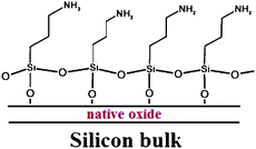
Although interesting sensing applications have been experimentally demonstrated by employing silanized silicon surfaces, the SiO2 layer introduces some physical constraints in biomolecular sensing. In fact, sensor performance may be limited by native oxide layers due to interfacial trapped states, which can cause hysteresis in the sensing response. In addition, in the case of thermal oxide layers, the receptor–analyte binding events take place far away from the sensor surface, reducing the light–analyte interaction and, consequently, the device sensitivity. To this aim, an hydrogen-terminated silicon surface represents a valid and novel alternative in chemical functionalization protocols. In particular, any SiO2 layer is etched from the silicon surface in hydrogen fluoride aqueous solution (1% HF, 40% NH4F), leaving the surface silicon atoms covalently bounded to hydrogen. In conclusion, several kinds of organic compounds can be bound to H–Si groups by the so-called hydrosilylation of the H-terminated silicon surface (see Fig. 17).
 | ||
| Fig. 17 Hydrosilylation of a H-terminated silicon surface. | ||
In summary, a lot of research efforts have been performed and are still being done in order to improve the photonic sensor capability of selectively binding target molecules, proteins, cells and nucleic acids to the functionalized silicon sensor surface. This chemical prerogative is oriented to develop biochemical techniques able to engineer the surface functionalization chemical processes for the particular analyte to be label-free detected without altering its chemical properties.72
Advanced resonant architectures for photonic biochemical sensing
Biochemical sensors based on planar resonant microcavities
Photonic sensors based on planar ring resonators have been widely employed in biochemical label-free detection. In fact, as described in the previous sections, a number of waveguide structures and materials have been investigated in order to improve sensing performance. The state of the art of these biochemical sensors involves novel sophisticated architectures, as well as the integration of microfluidic systems (e.g., micro-valves, micro-channels, micro-pumps, microfluidic mixers) for controlling fluids at the microscale.73 In this context, the research field named Optofluidics (i.e., the integration of optics and microfluidics in microsystems) represents an intriguing opportunity for enhancing sensing performance in several application fields, such as health, energy, food quality control, environment and safety, to name a few.74 Micro- and nanofluidic systems can be fabricated using conventional techniques, such as photolithography, lithography, X-ray lithography and laser micromachining. In this context, C. F. Carlborg et al. have designed and fabricated an array of optical slot-waveguide ring resonator sensors integrated with a PDMS microfluidic system for multiplexed real-time and label-free biosensing.75 The photonic sensor characterized by a chip area as small as 3 × 7 mm2 has been experimentally tested by exposing the sensible area to different ethanol and methanol concentrations. In addition, the time trace of increasing concentrations of anti-BSA binding to the glutaraldehyde-coated transducer has been carried out. The proposed sensor exhibits a volume refractive index detection limit of 5 × 10⁻⁶ RIU and a surface mass detection limit as low as 0.9 pg mm−2.Soft lithography represents a conventional and efficient fabrication technique for defining microfluidic channels in soft polymers with ultra high precise patterns. The elastomer PDMS has been widely employed for microfluidic system fabrication because of its bio-compatibility and transparency.76 Moreover, PDMS hydrophobic surface properties can be altered in an oxygen plasma by replacing some of the surface methyl groups (CH3) by hydroxyl groups (–OH).9 Consequently, the activated surface can form covalent siloxane bonds when in contact with silicon substrates, resulting in a stable and robust sensor chip. Finally, the PDMS flexibility can be employed for the fabrication of micro-pumps and valves, but, at the same time, this property can cause some damage, such as the irreversible microfluidic channel collapsing. In order to avoid this undesired effect, the minimum PDMS channel size is typically of tens of microns.77
Similar investigations have also been presented by J. Flueckiger et al.9 In fact, a photonic sensor based on cascaded ring resonators with a PDMS microfluidic system has been designed, exhibiting a sensitivity of ∼40 nm RIU−1 by exposing the sensible area to different concentrations of water/glycerin solution.
K. M. De Vos et al. have proposed a micron-sized integrated SOI optical biosensor based on a microring cavity for real time and sensitive measurements of the avidin/biotin system dynamics.78 Biotin has been properly immobilized on the amino-functionalized silicon surface. Consequently, the functionalized sensor surface has been exposed to an avidin solution using a flow cell mounted on the chip, and connected through tubings to a peristaltic pump. In this way, the authors have demonstrated that the optical microring resonator characterized by a ring radius of 5 μm is able to detect a bulk refractive index of 10−4 RIU. Moreover, protein concentrations down to 50 ng mL−1 can be sensed with good repeatability.
Interesting results have also been achieved in DNA and RNA detection.79 In fact, A. J. Qavi et al. have proposed a silicon photonic microring resonator array transduction platform for sensitive detection of microRNAs (miRNAs).70 In particular, chemical solutions have been controlled on the sensor surface via a 0.007-inch thick Maylar microfluidic gasket,80 sandwiched between a Teflon cartridge and the sensor chip. In this way, the proposed sensor is able to detect microRNA concentrations as low as 10 pM (i.e., 350 amol).
Generally, the accurate diagnosis of a disease state requires the detection and quantification of multiple biological markers. In this context, sensing platforms based on SOI ring resonator arrays integrated with microfluidic systems are suitable for this aim. For example, Washburn et al. have proposed a single microring sensor array for the parallel analysis of multiple biomarkers.81 In particular, prostate-specific antigen (PSA), α-fetoprotein (AFP), carcinoembryonic (CEA), tumor necrosis factor-α (TNF-α) and interleukin-8 (IL-8) have been detected at clinical concentrations. In conclusion, concentrations of cancer biomarkers CA15-3, HER2/ECD, CEA and TNF-α have been successfully detected in the clinical range 1–200 ng mL−1.82
The integration of microfluidic systems with advanced photonic resonant architectures represents an actual strategic approach for design and fabrication of ultra-high performance sensor chips. In this context, it is possible to mention same intriguing solutions generally based on the integration of multiple resonant microcavities.
The use of cascaded ring resonators in a photonic integrated chip has been demonstrated to be very useful for achieving ultra high sensing performance (see Fig. 18). In particular, the advantage of employing a multiple ring resonator architecture based on the Vernier effect consists of the possibility of amplifying the sensing performance normally achievable with a single ring resonator by a gain factor, G.
 | ||
| Fig. 18 The top view of a multiple ring resonator architecture based on the Vernier effect. | ||
According to Fig. 18, in such architectures one ring resonator acts as a filter, while the second one acts as a sensor, being directly exposed to the sensible area.22 In particular, an example of the Vernier spectrum exhibited by a double ring resonator architecture characterized by ring resonator perimeters LSensor = 1.212 mm and LFilter = 887.4 μm for sensor and filter rings, respectively, is plotted in Fig. 19.
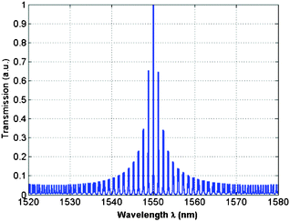 | ||
| Fig. 19 The Vernier spectrum of the cascaded ring resonator architecture. | ||
In detail, referring to eqn (5) and (6), it is possible to formulate the amplified sensing performance in terms of wavelength sensitivity SVernier and resonant wavelength shift ΔλVernier of the Vernier spectrum, as:
 | (16) |
In particular, FSRFilter is the free spectral range of the ring resonator acting as a filter, ΔFSR is equal to |FSRFilter − FSRSensor|, being FSRsensor the free spectral range of the ring resonator acting as a sensor. Interesting performance have been theoretically and experimentally demonstrated in chemical and biochemical detection. For example, a sensitivity as high as 2.91 × 10⁵ nm RIU−1 and a LOD of ∼10−6 RIU have been achieved by a digital optical sensor based on cascaded ring resonators with high Q-factors.83 Different concentrations of salt solutions in water have been detected using a cascaded-ring sensor with suspended Si-nanowire in SOI technology, revealing a sensitivity of 4.62 × 10⁵ nm RIU−1 and a LOD of 4.8 × 10⁻⁶ RIU.84 A sensitivity as high as 2169 nm RIU−1 has been experimentally demonstrated by measuring the flow between deionized water and aqueous solutions of NaCl with different concentrations.85 Moreover, the detection of different ethanol concentrations in water has been tested, revealing a sensitivity of 1300 nm RIU−1.86 In conclusion, photonic sensors based on the Vernier effect have been theoretically investigated for m-xylene and Pb(II) detection in water. A sensitivity as high as 149.74 μm RIU−1 with a LOD of ∼4 × 10⁻⁶ RIU and a sensitivity of 182.36 μm RIU−1 with a LOD as low as 3.5 × 10⁻⁶ RIU allows us to detect m-xylene concentrations lower than 60 ppm and Pb(II) concentrations lower than 50 ppb, respectively.87
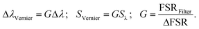
Another interesting solution based on the use of multiple resonance architectures consists of the dual cavity architecture, where a ring resonator or a racetrack resonator microcavity is coupled with a Fabry-Perot microcavity, as reported in Fig. 20.
 | ||
| Fig. 20 A schematic representation of a microring resonator integrated into a Fabry-Perot cavity.88 | ||
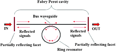
The advantage of designing such architectures consists of the generation of the well-known Fano resonance, due to complex interference revealed in the coupled structure, as formed by the Fabry-Perot cavity between the partially reflecting elements and the ring resonator. In Fig. 21, a useful comparison between the conventional Lorentzian line-shape resonant peek obtained with a single ring resonator and the Fano line-shape resonant peak is sketched. Both curves have been calculated as a function of the wavelength detuning with respect to the resonant wavelength λres.
 | ||
| Fig. 21 An illustration of the asymmetric Fano line-shape with respect to the typical Lorentzian line-shape of a standard ring resonator. | ||
As it is possible to appreciate in Fig. 21, the asymmetric Fano line-shape is characterized by a resonant peak steeper than the Lorentzian one. Consequently, the slope of its line-shape is much higher than that exhibited by the Lorentzian one. This feature results in the sensor capability to resolve smaller resonant wavelength shifts with respect to conventional sensors based on the single ring resonator (see Fig. 4). To this purpose, Yi et al. have proposed a microring resonator in SOI technology coupled with a Fabry-Perot cavity characterized by a length of 10 mm. The sensor exhibits a quality factor Q = 3.8 × 10⁴ and a limit of detection as low as ∼10−8 RIU.88 Biochemical sensors based on polymer microrings with sharp asymmetrical resonance have been proposed for monitoring different concentrations of glucose solution. Sensors proposed are able to detect a minimal concentration of glucose solution as low as 24 mg dL−1.89
In conclusion, other resonance microcavities can be employed for the design and fabrication of photonic sensors based on the asymmetric Fano line-shape. In this context, resonant microdisks90,91 and nanoscale plasmonic nanostructures92 have been investigated for designing photonic configurations able to produce Fano-resonances for high performance sensing.
Optical biosensors based on photonic crystals (PhCs) have been widely used for chemical and biochemical sensing because of their capability of exhibiting strong optical field confinement of light to a very small volume. Materials usually employed for the fabrication of planar PhC devices are heteroepitaxial layers, such as AlGaAs/GaAs, III-nitride compound layers or dielectric layers such as Si3N4, TiO2, SiO2 and the well-known SOI wafers.93 In addition, organic compounds, polymers and porous silicon have been also proposed for the fabrication of PhC sensors for organic vapour sensing.94
A planar PhC is characterized by a period arrangement of dielectric material in two dimensions. By properly designing the periodicity and symmetry of the crystal and the dielectric constants of the employed materials, it is possible to concentrate light at a precise wavelength and into extremely small volumes, producing very high local electromagnetic field intensities. In addition, by introducing a local defect in the periodic structure forming the PhC, it is possible to realize photonic waveguides and ultra-compact microcavities to be employed for sensing applications. For example, a schematic of a slot microcavity realized into a circular-path holes PhC is sketched in Fig. 22.95
 | ||
| Fig. 22 Top (a) and cross-sectional (b) views of a slot resonant microcavity in a planar photonic crystal.95 | ||
In this context, arrays of PhC microcavities characterized by high Q values (i.e., Q ∼ 9300) in the bio-ambient phosphate buffered saline (PBS), can detect analyte concentrations as low as ∼98 attograms.96 These sensors fabricated on a silicon-chip-based platform allow high throughput and high sensitivity to be achieved. In addition, a PhC microcavity sensor characterized by a total area as low as 50 μm2 with an effective detection area of 0.272 μm2 has been designed and fabricated for label-free monitoring of protein binding in a physiological buffer.97 A limit of detection for anti-biotin less than 20 pM has been achieved, corresponding to less than 4.5 fg of bound material on the sensor surface and fewer than 80 molecules in the microcavity modal volume.
An ultra-sensitive two-dimensional photonic crystal microcavity biosensor has been theoretically and experimentally demonstrated by M. Lee and P. M. Fauchet.98 By measuring the redshift corresponding to the binding of glutaraldehyde and BSA, the sensor performance has been estimated, revealing the capability of the proposed sensor to detect a molecule monolayer with a total mass as small as 2.5 fg. Jagerska et al. have presented a photonic crystal air-slot cavity in SOI technology.99 The sensor has been tested by exposing the chip to different gases (i.e., N2, He, CO2). The high quality factor of the cavity (Q ∼2.6 × 10⁴) allows us to achieve an experimental wavelength sensitivity of 510 nm RIU−1 and LOD below 1 × 10⁻⁵ RIU.
In conclusion, PhC-based sensors can be efficiently integrated with microfluidic systems in order to achieve very high performance in ultra-compact chips.100 To this purpose, the detection of dissolved avidin concentrations as low as 15 nM or 1 μg ml−1 has been experimentally achieved using functionalized slotted photonic crystal cavities with integrated microfluidics.101 In particular, surface mass densities as low as 60 pg mm−2 can be detected with a cavity sensing surface area of ∼2.2 μm2.
Nowadays, several research efforts are carried out in order to further enhance PhC microcavity sensing performance and to fabricate ultra-compact chip-integrated microarrays for label free and multiplex assays.102,103
Definitely, the planar resonant microcavity represents a good candidate for the mass-scale production of chip scale integrated optical sensing systems. Moreover, the integration of optical sensors with microfluidic systems is a strategic technological solution for revolutionizing many application fields, in particular medical diagnostics, environmental monitoring and safety applications.73,104
Biochemical sensors based on non-planar resonant microcavities
In the field of photonic sensors based on non-planar resonant microcavities, liquid core optical ring resonators (LCORRs) actually assume a dominant role.105 As sketched in Fig. 23, the LCORR platform employs a thin-walled micro-sized capillary, made of glass (SiO2) or polymers. In particular, the capillary serves as a microfluidic channel for fluidic sample transport and the circular cross-section of the capillary constitutes a ring resonator that supports the circulating mode, called whispering gallery mode (WGM). The propagation of WGM is based on the total internal reflection (TIR) principle localized at both internal and external interfaces among the capillary (e.g., refractive index nSiO2 ≈1.5 in case of glass capillary) and surrounding media (e.g., external nair ≈1 and internal nwater ≈1.33). Sensing principles characterizing LCORRs are the same, as already described for planar ring resonators.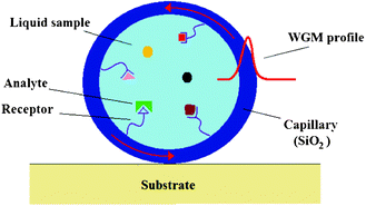 | ||
| Fig. 23 A cross-sectional view of a LCORR. | ||
In fact, as sketched in Fig. 23, internal capillary walls can be properly functionalized by immobilizing chemical receptors in order to enable the selective adsorption of target molecules dissolved in the fluid. Both homogeneous and surface sensing can induce a resonant WGM wavelength shift, which can be detected at the sensor output, as previously plotted in Fig. 4. Typically, WGMs can be launched into the capillary by placing the device in touch with the fiber taper, perpendicularly to the LCORR. In conclusion, the capillary dimensions (i.e., the ring radius) and the optical properties of employed materials determine the resonant wavelength, which characterizes the WGM spectrum.
Interesting LCORR chemical and biochemical applications have been presented in literature. For example, an optofluidic ring resonator (OFRR) has been fabricated and experimentally tested for the detection of 2,4-dinitrotoluene (DNT) vapour at room temperature.106 In particular, the capillary inner surface has been coated by a 60-nm-thick layer of poly(ethylene glycol) (PEG). Since WGM has a significant electric field inside and near the polymer layer, when vapour molecules are absorbed by the polymer the refractive index near the polymer surface changes and the thickness of the polymer layer increases, producing detectable WGM effective index changes. In this way, a wavelength sensitivity of 4.3 nm RIU−1 and a limit of detection as low as 200 pg of DNT have been demonstrated.
LCORRs are generally formed by stretching the central section of a fused silica capillary.107 In addition, such devices can be coated with a functionalized polymer on the inner surface for high performance sensing purposes.13,108 For example, biosensing experiments have been performed with BSA. In particular, a LCORR with a quality factor Q > 106 exhibits a sensitivity of 31 nm RIU−1, a bulk refractive index detection limit of 6 × 10⁻⁷ RIU, corresponding to a BSA mass detection limit of 0.5 pg mm−2.13
Zhu et al. have designed and fabricated an OFRR for sensitive label-free virus detection.109 In the experiment, filamentous bacteriophage M13 has been used as a safe model system. Moreover, the capillary inner surface has been coated with M13-specific antibodies. A detection limit of 2.3 × 10³ pfu mL−1 has been experimentally demonstrated with a sensitivity of 22 nm RIU−1. In addition, a concentration down to tens of viruses per mL and a surface density of only 5 × 105 cm−2 have been theoretically estimated.
A fused silica tube has been employed for the fabrication of a capillary-based OFRR for label-free small molecule detection.110 The LCORR is characterized by a Q-factor of 1.2 × 10⁵, exhibits a sensitivity of 570 nm RIU−1 and can detect a refractive index change as low as 2.8 × 10⁻⁷ RIU. This sensing performance allows us to detect 10 nM biotin with a surface mass density of 1.6 pg mm−2. Suter et al. have proposed for the first time an OFRR for the analysis of methylation in oligonucleotides using the MBD-2 (methyl binding) protein as capture molecule.111 This application assumes a fundamental role, since genomic methylation analysis is of great importance for cancer research and clinics. In fact, genomic methylation enables earlier cancer diagnosis prior to the point of metastasis. Finally, OFRR response has been characterized by artificially methylating ssDNA and dsDNA as a function of the number of methylated cytosine and DNA concentration.
S. M. Harazim et al. have recently proposed the fabrication of tubular rolled-up optofluidic ring resonators (i.e., RU-OFRRs) based on SiO2 material.112 The microfluidic integration of several RU-OFRRs on one chip is solved by enclosing the microtubes with a patterned robust SU-8 polymeric matrix. The sensor chip has been experimentally tested using several liquid solutions (i.e., DI water, PBS, PBS + 100 mM glucose, PBS + 200 mM glucose, PBS + 500 mM glucose) characterized by different refractive indices. A sensitivity as high as 800 nm RIU−1 and a limit of detection as low as 3.4 × 10⁻⁴ RIU have been calculated.
In conclusion, LCORRs can be integrated in a sensor array for multiplexed and label-free analysis.105 To this purpose, a schematic illustration is sketched in Fig. 24.
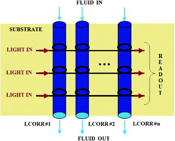 | ||
| Fig. 24 A schematic illustration of a LCORR sensor array.113 | ||
For example, a miniaturized and multiplexed sensor array based on LCORRs has been proposed by H. Zhu et al.113 The sensor has been exposed to different concentrations of glycerol/buffer solution, exhibiting a sensitivity of 20 nm RIU−1 and a detection limit as low as 10−6 RIU.
In summary, LCORRs represent an intriguing platform for advanced and high performance chemical and biochemical sensing, and a promising approach for developing novel instruments in analytical chemistry. In addition, processes and techniques usually employed for the LCORR fabrication allow both mass-scale production and microfluidics integration.
This part of the review on chemical and biochemical sensors based on non-planar resonant microcavities is completed by considering microsphere and microtoroid optical ring resonators. Also in these exotic photonic devices, the sensing principle consists of monitoring the WGM resonant wavelength shifts induced by effective index changes caused by the selective adsorption of target analytes to the microsphere and microtoroid surfaces, or by cover medium RI changes localized near the device surfaces. A schematic illustration of microspheres and microtoroids is sketched in Fig. 25.
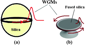 | ||
| Fig. 25 A schematic illustration of (a) microsphere and (b) microtoroid microcavities. | ||
The advantage of using spherical and toroidal microcavities consists in the possibility of achieving ultra high quality factors Q (e.g., Q ∼0.8 × 10¹⁰ in fused-silica microspheres114 and Q-factors above 30 million in silica microtoroids115). Recently, an optical quality-factor of silica microsphere as high as 7.5 × 10⁷ has been demonstrated at λ = 1.55 μm.116 In this way, the interaction between WGMs and analytes on sensor surface is significantly enhanced. For example, fused silica microring resonators can exhibit wavelength sensitivity of the order of 30 nm RIU−1, revealing a LOD of refractive index change of the order of 10−7 RIU.117 In addition, porous silicon microspheres have also been investigated and fabricated and can be applied as resonant microcavities for sensing purposes exhibiting interesting performances, as high as those previously reported for a fused silicon microsphere.118
The sensing technique generally consists of functionalizing the microsphere or microtoroid surfaces with chemical receptors in order to immobilize the target molecule to be detected. In this context, a silica microsphere sensor with radius of 91 μm and Q-factor as high as 5 × 10⁵ has been proposed for label-free small molecule detection. Experimental results demonstrate the sensor capability of detecting a change of 0.4 fmol silica molecule.119
High-Q optical microsphere sensors have been experimentally tested by functionalizing the sensor surfaces with cylindrical bacteria at random horizontal orientation.120 The proposed sensors exhibit a measured sensitivity of 1.2 × 10²E. coli mm−2, which correspond to ∼34 pg mm−2 dry-mass loading or a total of 44 bacteria bound to the sphere surface at a random location. Moreover, microsphere resonators have been proposed as label-free detectors for proteolytic activity. In particular, trypsin and BSA have been used as a model system, revealing a detection limit as low as 10−8 mg ml−1. In detail, a surface density of 17 pg mm−2 is achieved with a Q-factor of 2 × 105.121 Another interesting sensing application consists of functionalizing an optical microsphere resonator biosensor with an aptamer as the receptor for the measurement of biomolecule thrombin.122 The detection limit is estimated to be of the order of 1 NIH unit mL−1.
A fused silica microsphere ring resonator has also been proposed for mercuric ion Hg(II) detection in an aqueous environment, revealing a limit of detection of 50 ppb of Hg(II).123
Finally, microtoroid resonators have also been investigated revealing sensing performances similar to those previously described about microsphere sensors.124 Moreover, J. Zhu et al. have developed an accurate and efficient method for detecting and measuring individual nanospecies one-by-one (i.e., Influenza A (InfA) virions, PS and Au nanoparticles of various sizes) as they are adsorbed in the modal volume of a microtoroid resonator.125
In summary, although sensing performances can be significantly enhanced by employing microsphere and microtoroid resonators, microfluidics and photonics integration, multiplexed detection and mass-production are still very challenging. In any case, the intriguing potential of such photonic resonant architectures in sensing applications is actually the subject of intensive research efforts.126,127
Conclusions and future outlook
Nowadays, photonic resonant microcavities represent a suitable technological platform for the fabrication of chemical and biochemical photonic lab-on-a-chip. In fact, as analyzed in this review, several architectures based on resonant microcavities have been widely investigated in the last few years, exhibiting ultra high performances. The possibility of implementing arrays of resonant microcavities in a single chip and employing standard CMOS compatible processes for the fabrication of photonic integrated devices with microfluidic systems, enables real-time processing, multiplexed detection, high-throughput screening and point-of-care analysis with a single and cheap photonic sensor.Future developments of advanced sensor chips based on resonant microcavities are oriented to integrate optical sources and detectors together in the same photonic chip. In this way, sensor reliability and measurement accuracy and reproducibility, can be significantly improved. Moreover, further improvements in detection limits depend on surface functionalization chemistries too. In this context, improvements of functionalizing chemical techniques lead to minimize non-specific binding on the sensor surface, resulting in enhanced sensor selectivity.
Recently, optical sensors based on resonant microcavities have been investigated and designed for optical particle transporting, storing, sensing and manipulation. For example, a SOI slot waveguide has been proposed for trapping and transporting 75-nm dielectric nanoparticles and 1-DNA molecules.128 In this context, resonant microcavities play a dominant role. In fact, a microring resonator architecture based on SU-8 solid-core waveguides can be integrated with a PDMS optofluidic system for constituting an optofluidic switch for particle trapping.129 The authors have demonstrated the sensor capability to achieve a 250% enhancement of the steady-state velocity of trapped particles along with an 80% switching fraction.
S. Lin et al. have demonstrated the trapping of particles using multiple planar silicon microring resonators. All-optical control of micro-particles with the ability to quantitatively store particles on a microring and switch them between rings has been experimentally demonstrated.130 In conclusion, N. Lagos et al. have proposed a numerical investigation of a sensor based on two silicon resonant microdisks. In particular, the sensor proposed is characterized by a sensitivity proportional to the gap between two microdisks. The optimized configuration is able to sense the presence of one nanoparticle characterized by a size as small as 10 nm.131 Finally, the manipulation of micro- and nanometre size chemical species (e.g., nanoparticles, molecules, live cells, to name a few) with high performance sensing capabilities, identify the direction of recent research efforts. In fact, these advanced optical lab-on-a-chip technologies can significantly revolutionize a number of sensor applications, in biology, medicine, pharmaceuticals and biotechnologies.127
From a technological point of view, the most intriguing platform for the fabrication of integrated sensors based on resonant microcavities is SOI. Moreover, among several configurations investigated in this review (e.g., PhC-based microcavities, microspheres, microtoroids, LCORR), planar ring resonators have been assumed a predominant role in the last few years. In fact, they can be easily fabricated on a SOI wafer by employing standard facilities and processes already developed for micro- and nano-electronics integrated circuit fabrication. The main drawback characterizing photonic sensors based on integrated microcavities is represented by the strong dependence of sensing performance on optical properties of materials and geometrical parameters characterizing the photonic device (e.g., the length of the microcavity and the coupling length of directional couplers characterizing planar ring resonators, to name two). In addition, the high refractive index contrast of the oxide/silicon/air material system makes silicon waveguides (e.g., wire, rib and slot waveguides) vulnerable to any fabrication imperfections, such as surface roughness on waveguide sidewalls and the presence of scattering sites. Consequently, these effects induce relevant changes in resonance wavelengths and the quality factor of the microcavity, resulting in worse performance of sensor operation.
In this context, research efforts are actually oriented to improve the quality of technological processes and enhance the fabrication tolerances. In addition, sophisticated design and simulation methods and algorithmic models are needed for investigating the effects of chemical/biochemical particles and fluids injected by the microfluidic system in integrated photonic devices. In fact, a lot of environmental parameters, such as temperature, humidity, chemical liquid pH and particle sizes to be detected, can strongly influence the optical properties of silicon waveguides.
In conclusion, the optofluidic lab-on-chip research field undoubtedly identifies a multidisciplinary research community, encompassing engineers, physicists, chemists, biologists and technologists. In this context, the design and fabrication of complex lab-on-chip devices can be surely encouraged by ensuring the accessibility of sophisticated simulations software to all professional figures mentioned above, in order to strategically converging different technical competencies. In the near future, the integration of photonic integrated microcavities and microfluidics will lead to the implementation of commercial lab-on-chip devices based on array-format detection for high-throughout screening for advanced chemical and biochemical sensing.
References
- S. Janz, A. Densmore, D. X. Xu, W. Sinclair, J. H. Schmid, R. Ma, M. Vachon, J. Lapointe, A. Delage, E. Post, Y. Li, T. Mischki, G. Lopinski, P. Cheben and B. Lamontagne, 6th IEEE Int. Conf. on Group IV Photonics, 2009, 89-91 Search PubMed ISBN: 978-1-4244-4403-8.
- S. Dante, D. Duval, A. B. Gonzalez Guerrero, J. Osmond, K. Zinoviev, B. Sepulveda, C. Dominguez and L. M. Lechuga, Optica Pura y Aplicada, 2012, 45, 87–95 CrossRef.
- A. Densmore, D.-X. Xu, S. Janz, P. Waldron, T. Mischki, G. Lopinski, A. Delage, J. Lapointe, P. Cheben, B. Lamontagne and J. H. Schmid, Opt. Lett., 2008, 33, 596–598 CrossRef CAS.
- X. Fan, I. M. White, H. Zhu, J. D. Suter and H. Oveys, Proc. SPIE, 2007, 6452(64520M), 1–20 Search PubMed.
- W. Bogaerts, P. De Heyn, T. Van Vaerenbergh, K. De Vos, S. K. Selvaraja, T. Claes, P. Dumon, P. Bienstman, D. Van Thourhout and R. Baets, Laser Photonics Rev., 2012, 6, 47–73 CrossRef CAS.
- Y. Sun and X. Fan, Anal. Bioanal. Chem., 2011, 399, 205–211 CrossRef CAS.
- C.-Y. Chao and L. J. Guo, J. Lightwave Technol., 2006, 24, 1395–1402 CrossRef CAS.
- K. De Vos, I. Bertolozzi, E. Schacht, P. Bienstman and R. Baets, Opt. Express, 2007, 15, 7610–7615 CrossRef.
- J. Flueckiger, S. M. Grist, G. Bisra, L. Chrostowski and K. C. Cheung, Proc. of SPIE, 2011, 7929, 79290I CrossRef.
- J. Saunders, M. A. Dreher, J. A. Barnes, C. M. Crudden, J. Du, H. Loock, D.-X. Xu, A. Densmore, R. Ma, S. Janz, M. Vachon, J. Lapointe, A. Delage, J. Schmid and P. Cheben, Conf. Proc. 7th IEEE Group IV Photon. (GFP), 2010, 177-179 Search PubMed ISBN: 978-1-4244-6346-6.
- I. M. White and X. Fan, Opt. Express, 2008, 16, 1020–1028 CrossRef.
- V. M. N. Passaro, F. Dell'Olio and F. De Leonardis, Sensors, 2007, 7, 2741–2749 CrossRef CAS.
- H. Zhu, I. M. White, J. D. Suter, P. S. Dale and X. Fan, Opt. Express, 2007, 15, 9139–9146 CrossRef CAS.
- M. Fukuyama, Y. Amemiya, Y. Abe, Y. Onishi, A. Hirowatari, K. Terao, T. Ikeda, A. Kuroda and S. Yokoyama, Jap. J. Appl. Phys., 2011, 50, 04DL11-1–04DL11-5 Search PubMed.
- N. A. Yebo, P. Lommens, Z. Hens and R. Baets, Opt. Express, 2010, 18, 11859–11866 CrossRef CAS.
- H. Zhao, P. H. Brown and P. Schuck, Biophys. J., 2011, 100, 2309–2317 CrossRef CAS.
- W. Knoll, Annu. Rev. Phys. Chem., 1998, 49, 569–638 CrossRef CAS.
- J. Voros, Biophys. J., 2004, 87, 553–561 CrossRef.
- H. N. Daghestani and B. W. Day, Sensors, 2010, 10, 9630–9646 CrossRef CAS.
- V. M. N. Passaro, B. Troia, M. La Notte and F. De Leonardis, Advances in Chemical Sensors, (W. Wang Ed.), In-Tech Publisher, Shanghai, 2012, ISBN: 978-953-307-792-5 Search PubMed.
- V. M. N. Passaro, B. Troia and F. De Leonardis, Sensors & Transducers Journal, 2012, 14-1, 212–230 CAS.
- V. M. N. Passaro, B. Troia and F. De Leonardis, Sens. Actuators, B, 2012, 168, 402–420 CrossRef CAS.
- Z. Hu, A. Zhang, G. Storz, S. Gottesman and S. H. Leppla, Nucleic Acids Res., 2006, 34, e52 CrossRef.
- L. Szekvolgyi, Z. Rakosy, B. L. Balint, E. Kokai, L. Imre, G. Vereb, Z. Bacso, K. Goda, S. Varga, M. Baòazs, V. Dombradi, L. Nagy and G. Szabo, Proc. Natl. Acad. Sci. U. S. A., 2007, 104, 14964–14969 CrossRef.
- J. T. Kirk, G. E. Fridley, J. W. Chamberlain, E. D. Christensen, M. Hochberg and D. M. Ratner, Lab Chip, 2011, 11, 1372–1377 RSC.
- B. Sciacca, F. Frascella, A. Venturello, P. Rivolo, E. Descrovi, F. Giorgis and F. Geobaldo, Sens. Actuators, B, 2009, 137, 467–470 CrossRef.
- L. Le, M. Suihua, J. Yanhong, C. Xinyuan, L. Zhiyi, H. Yonghong and G. Jihua, Rev. Sci. Instrum., 2011, 82, 023109 CrossRef.
- E. Mauriz, A. Calle, J. J. Manclus, A. Montoya and L. M. Lechuga, Anal. Bioanal. Chem., 2007, 387, 1449–58 CrossRef CAS.
- A. Q. Liu, H. J. Huang, L. K. Chin, Y. F. Yu and X. C. Li, Anal. Bioanal. Chem., 2008, 391, 2443–52 CrossRef CAS.
- L. Liu, N. Xia and J. Wang, RSC Adv., 2012, 2, 2200–2204 RSC.
- R. Jha and A. K. Sharma, Sens. Actuators, B, 2010, 145, 200–204 CrossRef.
- L. Zhou, X. Sun, X. Li and J. Chen, Sensors, 2011, 11, 6856–6867 CrossRef CAS.
- K. Q. Le and P. Bienstman, 15th Annual Symp. of IEEE Photon. Benelux Chapter, 2010 Search PubMed.
- Y. Chen, Z. Xu, L. Liu and J.-P. Coppe, IEEE Sensors 2010 Conf., 2010, 2295–2298 Search PubMed , ISBN: 978-1-4244-8168-2.
- M. Jin, H. Van Wolferen, H. Wormeester, A. Van Den Berg and E. T. Carlen, Nanoscale, 2012, 4, 4712–4718 RSC.
- I. M. White, J. Gohring and X. Fan, Opt. Express, 2007, 15, 17433–17442 CrossRef CAS.
- F. De Leonardis and V. M. N. Passaro, New J. Phys., 2007, 9, 1–25 CrossRef.
- V. M. N. Passaro and F. De Leonardis, Sensors, 2009, 9, 7814–7836 CrossRef CAS.
- F. Dell'Olio and V. M. N. Passaro, Opt. Express, 2007, 35, 4977–4993 CrossRef.
- H. Yamada and T. Chu, PIERS Online, 2009, 5, 125–128 CrossRef.
- S. Lardenois, D. Pascal, L. Vivien, E. Cassan and S. Laval, Opt. Lett., 2003, 28, 1150–1152 CrossRef CAS.
- S. Xiao, M. H. Khan, H. Khan, H. Shen and M. Qi, Opt. Express, 2007, 15, 14467–14475 CrossRef.
- H. Zhang, J. Zhang, S. Chen, J. Song, J. S. Kee, M. Yu and G.-Q. Lo, IEEE Photonics Technol. Lett., 2012, 24, 10–12 CrossRef CAS.
- X. Fan, Advanced Photonic Structures for Biological and Chemical Detection, Springer, New York, 2009 Search PubMed.
- D.-X. Xu, A. Densmore, A. Delage, P. Waldron, S. Janz, J. Lapointe, G. Lopinski, T. Mischki, R. McKinnon, P. Cheben and J. H. Schmid, Opt. Express, 2008, 16, 15137–15148 CrossRef CAS.
- S. Malathi, K. E. Rani, U. Raghunath and T. Srinivas, ICP2010, 2010, 51, 1–3 Search PubMed.
- F. Dell'Olio, V. M. N. Passaro and F. De Leonardis, Proc. of 8th International Conference on Transparent Optical Networks, 2006, 4, 128–131 CAS.
- A. Densmore, D.-X. Xu, P. Waldron, S. Janz, P. Cheben, J. Lapointe, A. Delage, B. Lamontagne, J. H. Schimd and E. Post, IEEE Photonics Technol. Lett., 2006, 18, 2520–2522 CrossRef CAS.
- V. M. N. Passaro, M. La Notte, B. Troia, L. Passaquindici, F. De Leonardis and G. Giannoccaro, IJRRAS, 2012, 11, 411–427 CAS.
- F. De Leonardis, G. Giannoccaro, B. Troia, V. M. N. Passaro and A. G. Perri, IWASI, 2011, 142-147 Search PubMed ISBN: 978-1-4577-0624-0.
- C. A. Barrios, Sensors, 2009, 9, 4751–4765 CrossRef CAS.
- C. A. Barrios, K. B. Gylfason, B. Sanchez, A. Griol, H. Sohlstrom, M. Holgado and R. Casquel, Opt. Lett., 2007, 32, 3080–3082 CrossRef CAS.
- C. A. Barrios, M. J. Banuls, V. Gonzalez-Pedro, K. B. Gylfason, B. Sanchez, A. Griol, A. Maquieira, H. Sohlstrom, M. Holgado and R. Casquel, Opt. Lett., 2008, 33, 708–710 CrossRef CAS.
- T. Claes, J. G. Molera, K. De Vos, E. Schacht, R. Baets and P. Bienstman, IEEE Photonics J., 2009, 1, 197–204 CrossRef.
- G. Z. Mashanovich, M. M. Milosevic, M. Nedeljkovic, N. Owens, B. Xiong, E. J. Teo and Y. Hu, Opt. Express, 2011, 19, 7112–7119 CrossRef CAS.
- J. Halldorsson, N. B. Arnfinnsdottir, A. B. Jonsdottir, B. Agnarsson and K. Leosson, Opt. Express, 2010, 18, 16217–16226 CrossRef CAS.
- C.-Y. Chao, W. Fung and L. J. Guo, IEEE J. Sel. Top. Quantum Electron., 2006, 12, 134–142 CrossRef CAS.
- H. Sun, A. Chen and L. R. Dalton, IEEE/LEOS, 2009, 22-22 Search PubMed ISBN: 978-1-4244-2382-8.
- A. Kargar and C. Lee, 9th IEEE Conf. on Nanotechnology, 2009, 240-242 Search PubMed ISBN: 978-1-4244-4832-6.
- H. Sun, A. Chen and L. R. Dalton, IEEE Photonics J., 2009, 1, 48–57 CrossRef.
- H.-S. Lee, G.-D. Kim and S.-S. Lee, CLEO/PACIFIC RIM, 2009, 1-2 Search PubMed ISBN: 978-1-4244-3830-3.
- S. Li, J. Huang and L. Cai, Nanotechnology, 2011, 22, 425502 CrossRef.
- M. Mancuso, J. M. Goddard and D. Erickson, Opt. Express, 2011, 20, 245–255 CrossRef.
- N. A. Yebo, S. P. Sree, E. Levrau, C. Detavernier, Z. Hens, J. A. Martens and R. Baets, Opt. Express, 2012, 20, 11855–11862 CrossRef CAS.
- B. Troia, V. M. N. Passaro and F. De Leondardis, Conf. Proc. of 19th Telecomm. Forum, 2011, 778–781, Search PubMed ISBN: 978-1-4577-1498-6.
- V. M. N. Passaro and M. La Notte, Sensors, 2012, 12, 2436–2455 CrossRef.
- J.-Y. Byeon, Application of silicon photonic microring resonators to the study of surface bioconjugation and protein capture agent binding kinetics, Ph.D. thesis, University of Illinois at Urbana-Champaign, 2011 Search PubMed.
- M. S. Luchansky and R. C. Bailey, Anal. Chem., 2010, 82, 1975–1981 CrossRef CAS.
- R. C. Bailey, A. L. Washburn, A. J. Qavi, M. Iqbal, M. Gleeson, F. Tybor and L. C. Gunn, Proc. SPIE, 2009, 7220, 72200N CrossRef.
- A. J. Qavi, J. T. Kindt, M. A. Gleeson and R. C. Bailey, Anal. Chem., 2011, 83, 5949–5956 CrossRef CAS.
- Z. Wang and G. Jin, J. Biochem. Biophys. Methods, 2003, 57, 203–211 CrossRef CAS.
- A. K. Mudraboyina and J. Sabarinathan, Sensors, 2011, 11, 11295–11304 CrossRef CAS.
- J. Wu and M. Gu, J. Biomed. Opt., 2011, 16, 080901 CrossRef.
- Y.-F. Chen, L. Jiang, M. Mancuso, A. Jain, V. Oncescu and D. Erickson, Nanoscale, 2012, 4, 4839 RSC.
- C. F. Carlborg, K. B. Gylfason, A. Kazmierczak, F. Dortu, M. J. Banuls Polo, A. Maquieira Catala, G. M. Kresbach, H. Sohlstrom, T. Moh, L. Vivien, J. Popplewell, G. Ronan, C. A. Barrios, G. Stemme and W. van der Wijngaart, Lab Chip, 2010, 10, 281–290 RSC.
- L. Chrostowski, S. Grist, J. Flueckiger, W. Shi, X. Wang, E. Ouellet, H. Yun, M. Webb, B. Nie, Z. Liang, K. C. Cheung, S. A. Schmidt, D. M. Ratner and N. A. F. Jager, Proc. SPIE, 2012, 8236, 823620 CrossRef.
- H. K. Hunt and A. M. Armani, Nanoscale, 2010, 2, 1544–1559 RSC.
- K. M. De Vos, I. Bartolozzi, P. Bienstman, R. Baets and E. Schacht, Proc. of SPIE, 2007, 6447, 64470 K-1–64470 K-8 Search PubMed.
- A. L. Washburn, J. Gomez and R. C. Bailey, Anal. Chem., 2011, 83, 3572–3580 CrossRef CAS.
- A. L. Washburn, L. C. Gunn and R. C. Bailey, Anal. Chem., 2009, 81, 9499–506 CrossRef CAS.
- A. L. Washburn, M. Luchansky, A. Bowman and R. C. Bailey, Anal. Chem., 2009, 82, 69–72 CrossRef.
- H. Zhu, P. S. Dale, C. W. Caldwell and X. Fan, Anal. Chem., 2009, 81, 9858–9865 CrossRef CAS.
- L. Jin, M. Li and J.-J. He, Opt. Commun., 2011, 284, 156–159 CrossRef CAS.
- J. Hu and D. Dai, IEEE Photonics Technol. Lett., 2011, 23, 842–844 CrossRef CAS.
- T. Claes, W. Bogaerts and P. Bienstman, Opt. Express, 2010, 18, 22747–22761 CrossRef CAS.
- D. Dai, Opt. Express, 2009, 17, 23817–23822 CrossRef CAS.
- B. Troia, V. M. N. Passaro, F. De Leonardis and A. V. Tsarev, 16th Eur. Conf. on Int. Opt., 2012, ECIO Search PubMed.
- H. Yi, D. S. Citrin and Z. Zhou, Opt. Express, 18, 2967–2972 CrossRef CAS.
- C.-Y. Chao and L. J. Guo, Appl. Phys. Lett., 2003, 83, 1527–1529 CrossRef CAS.
- V. M. N. Passaro and F. De Leonardis, IEEE J. Sel. Top. Quantum Electron., 2006, 12, 124–133 CrossRef CAS.
- V. M. N. Passaro, B. Casamassima, F. De Leonardis, F. Dell'Olio and F. Magno, IWASI 2007, 2007, 1-6 Search PubMed ISBN: 978-1-4244-1245-7.
- L. Niu, J. B. Zhang, Y. H. Fu, S. Kulkarni and B. Luky Anchuk, Opt. Express, 2011, 19, 22974–81 CrossRef.
- D. Biallo, A. D'Orazio, M. De Sario, V. Marrocco, V. Petruzzelli and F. Prudenzano, 2006 International Conference on Transparent Optical Networks, 2006, 2, 44–48 CrossRef.
- M. J. Sweetman and N. H. Voelcker, RSC Adv., 2012, 2, 4620–4622 RSC.
- T. Yoshie, L. Tang and S.-Y. Su, Sensors, 2011, 11, 1972–1991 CrossRef.
- Y. Zou, S. Chakravarty, W.-C. Lai, C.-Y. Lin and R. T. Chen, Lab Chip, 2012, 12, 2309–2312 RSC.
- S. Zlatanovic, L. W. Mirkarimi, M. M. Sigalas, M. A. Bynum, E. Chow, K. M. Robotti, G. W. Burr, S. Esener and A. Grot, Sens. Actuators, B, 2009, 141, 13–19 CrossRef.
- M. Lee and P. M. Fauchet, Opt. Express, 2007, 15, 4530–4535 CrossRef CAS.
- J. Jagerska, H. Zhang, Z. Diao, N. Le Thomas and R. Houndrè, Opt. Lett., 2010, 35, 2523–2525 CrossRef.
- C. J. Choi and B. T. Cunningham, Lab Chip, 2006, 6, 1373–1380 RSC.
- M. G. Scullion, A. Di Falco and T. K. Krauss, Biosens. Bioelectron., 2011, 27, 101–105 CrossRef CAS.
- S. Chakravarty, W.-C. Lai, Y. Zou and R. T. Chen, Proc. SPIE, 2012, 8212, 82120A CrossRef.
- F. Hosseinibalam, S. Hassanzadeh, A. Ebnali-Heidari and C. Karnutsch, Appl. Opt., 2012, 51, 568–576 CrossRef CAS.
- N. Jokerst, M. Royal, S. Palit, L. Luan, S. Dhar and T. Tyler, J. Biophotonics, 2009, 2, 212–226 CrossRef CAS.
- X. Fan, I. M. White, H. Zou, J. D. Suter and H. Oveys, Proc. SPIE, 2007, 6452, 6452M Search PubMed.
- Y. Sun, J. Liu, G. Frye-Mason, S.-J. Ja, A. K. Thompson and X. Fan, Analyst, 2009, 134, 1386–1391 RSC.
- S. I. Shopova, J. M. Cupps, P. Zhang, E. P. Henderson, S. Lacey and X. Fan, Opt. Express, 2007, 15, 12735–12742 CrossRef CAS.
- I. M. White, H. Oveys and X. Fan, Opt. Lett., 2006, 31, 1319–1321 CrossRef.
- H. Zhu, I. M. White, J. D. Suter, M. Zourob and X. Fan, Analyst, 2008, 133, 356–360 RSC.
- H. Li and X. Fan, Appl. Phys. Lett., 2010, 97, 011105–011105-3 CrossRef.
- J. D. Suter, D. J. Howard, H. Shi, C. W. Caldwell and X. Fan, Biosens. Bioelectron., 2010, 26, 1016–1020 CrossRef CAS.
- S. M. Harazim, V. A. Bolanos, S. Kiravittaya, S. Sanchez and O. G. Schmidt, Lab Chip, 2012, 12, 2649–2655 RSC.
- H. Zhu, I. M. White, J. D. Suter, M. Zourob and X. Fan, Anal. Chem., 2007, 79, 930–937 CrossRef CAS.
- M. L. Gorodetsky, A. A. Savchenkov and V. S. Ilchenko, Opt. Lett., 1996, 21, 453–455 CrossRef CAS.
- M. Hossein-Zadeh and K. J. Vahala, Opt. Express, 2007, 15, 166–175 CrossRef.
- J.-B. Jager, V. Calvo, E. Delamadeleine, E. Hadji, P. Noe, T. Ricart, D. Bucci and A. Morand, Appl. Phys. Lett., 2011, 99, 181123–181123-3 CrossRef.
- N. M. Hanumegowda, C. J. Stica, B. C. Patel, I. White and X. Fan, Appl. Phys. Lett., 2005, 87, 201107–201107-3 CrossRef.
- R. Fenollosa, F. Ramiro-Manzano, M. Tymczenko and F. Meseguer, J. Mater. Chem., 2010, 20, 5210–5214 RSC.
- I. M. White, N. M. Hanumegowda and X. Fan, Opt. Lett., 2005, 30, 3189–3191 CrossRef CAS.
- H.-C. Ren, F. Vollmer, S. Arnold and A. Libchaber, Opt. Express, 2007, 15, 17410–17423 CrossRef.
- N. M. Hanumegowda, I. M. White, C. J. Stica, B. C. Patel, H. Oveys and X. Fan, Proc. SPIE, 2005, 6004, 60040I–600401-12 CrossRef.
- H. Zhu, J. D. Suter, I. M. White and X. Fan, Sensors, 2006, 6, 785–795 CrossRef CAS.
- N. M. Hanumegowda, I. M. White and X. Fan, Sens. Actuators, B, 2006, 120, 207–212 CrossRef.
- H. K. Hunt, C. Soteropulosa and A. M. Armani, Sensors, 2010, 10, 9317–9336 CrossRef CAS.
- J. Zhu, S. K. Ozdemir, L. He, D.-R.- Chen and L. Yang, Opt. Express, 2011, 19, 16195–16206 CrossRef CAS.
- M. Baaske and F. Vollmer, ChemPhysChem, 2012, 13, 427–436 CrossRef CAS.
- F. Vollmer and S. Roy, Journal of the Indian Institute of Science, 2012, 92(2), 233–251 CAS.
- H. J. Yang, S. D. Moore, B. S. Schmidt, M. Klug, M. Lipson and D. Erickson, Nature, 2009, 457, 71–75 CrossRef.
- A. H. J. Yang and D. Erickson, Lab Chip, 2010, 10, 769–774 RSC.
- S. Lin and K. B. Crozier, Lab Chip, 2011, 11, 4047–4051 RSC.
- N. Lagos and M. M. Sigalas, Sens. Actuators, B, 2011, 153, 252–255 CrossRef.
| This journal is © The Royal Society of Chemistry 2013 |