Step-by-step build-up of ordered p–n heterojunctions at nanoscale for efficient light harvesting†
Junfeng
Yan
ab,
Qian
Ye
a,
Xiuxun
Han
a and
Feng
Zhou
*a
aLanzhou Institute of Chemical Physics, Chinese Academy of Sciences, Lanzhou, 730000, China. E-mail: zhouf@lzb.ac.cn
bGraduate School, Chinese Academy of Sciences, Beijing, 100039, China
First published on 30th October 2012
Abstract
A simple “grafting from” strategy is reported to graft polymer brushes bearing thiophene groups onto TiO2 nanowires via a surface initiated polymerization and FeCl3 catalytic oxidized polymerization. Subsequently, the in situ CdS nanocrystals can be fabricated along the conductive polymer network, enabling highly ordered p–n heterojunctions to be prepared on the nanoscale. Polynorbornene bearing thiophene was grafted onto TiO2 nanowires via surface-initiated ring-opening metathesis polymerization (SI-ROMP), and then the oxidization polymerization of the thiophene derivative was performed to prepare conductive conjugated polythiophene brushes. The carboxyl groups in conductive polymer brushes can be used as the source precursor to coordinate cadmium cations for templating CdS nanocrystal formation, meanwhile creating intimate interfacial contact between nanocrystals and conjugated polymers. This novel approach offered a superior platform to the step-by-step build-up of ordered heterojunctions on the nanometer scale and has great advantages in precisely controlling the detailed nano-morphology and dispersion of nanocrystals within conductive polymers.
1. Introduction
Recent advances in the synthesis and application of conductive polymers (CPs) have stimulated increasing interest in exploiting CPs for the development of organic/inorganic photovoltaic platforms.1–9 The excellent properties of CPs such as their light weight, flexibility,10 excellent solution processability,11 tailorable electrochemical properties and high charge-carrier mobility have greatly expanded their usage in diverse areas including photovoltaics, light-emitting diodes (LEDs) and thin film transistors.12 Among these CPs, poly(3-hexylthiophene) (P3HT) is regarded as one of the most widely studied organic semiconductors for solar cells.13,14 Other than dye-sensitized solar cells and silicon solar cells,15–18 the emergence of semiconductor nanocrystals (NCs) with multiple exciton generation capability as the building blocks has afforded promising opportunities to deliver efficient solar energy conversion in next generation photovoltaic cells.19 Their quantum-confined nature allows us to manipulate the energy band gap of these NCs via size and shape control, in order to tune the photo response.20In order to combine the good mechanical flexibility and solution processability of CPs and the excellent photoactivity and high conductivity of NCs, organic/inorganic hybrid solar cells have gained widespread attention in recent years.21–25 Usually, CP/NC nanocomposites are prepared by simply physically mixing these two components, which are mainly in the interconnected phase-separated structured domains over the sub-20 nm length-scale.2,22,26 As such, it still remains a challenge to avoid severe nanoscale phase separation, which can lower the interfacial contact area and diminish the device performance, probably due to the interrupted charge transfer.24 In practice, the exciton formed after light is harvested and the separated charges could only travel less than 20 nm before recombination in organic–inorganic hybrid solar cells.27 An ideal configuration is the highly desirable bicontinuous and nanoscopic phase-separated mixture of CPs/NCs, limited to 20 nm, with strong electronic coupling between these two counterparts. Highly ordered orientation is key in achieving efficient charge separation and transport, but it is currently difficult to realize via the conventional blending approach due to the nature of the poorly defined interface. Thus, to solve microscopic phase separation problems is crucial in realizing efficient charge transfer and hence high photo conversion.28 Several approaches have been proposed such as co-solvent mixtures and surface modification of QDs; the most promising approach is chemical bond linking between QDs and polymers.29
Lin et al. have demonstrated P3HT linking with CdSe nanorods via the Heck coupling reaction for improved interfacial contact.30 Besides CdSe nanocrystals, CdS also can be used in P3HT-based hybrid solar cells.31–33 High density P3HT grafting silica via surface-initiated Kumada catalyst-transfer polycondensation,34 and chemical bonded p–n heterojunctions by surface initiated electrodeposition of p-type conducting polymer inside TiO2 nanotubes, both aimed at the improvement of interfacial adhesion.35 In this paper, we report a novel approach to fabrication of ordered p–n heterojunctions on the nanoscale by combining surface initiated polymerization36,37 with polymer brush templated nanocrystal fabrication to realize intimate contact nano-architecture, with the aim of efficiently promoting the charge transfer and light harvesting efficiency.
2. Experimental
TiO2 nanowires (100 mg) were immersed in 1.5 mg mL−1 solution (ultrapure water![[thin space (1/6-em)]](https://www.rsc.org/images/entities/char_2009.gif) :ethanol = 4:1) of initiator and stirred for 18 h in the dark at room temperature. The modified TiO2 nanowires were isolated and purified by repeated washing with ultrapure water and ethanol using centrifugation. Then the samples were dried under vacuum overnight at 40 °C. Firstly, the monomer of 5-norbornene-2-methanol-3-thiopheneacetic acid ester (NMTE) was polymerized on biomimetic initiator anchored TiO2 nanowires via ring-opening metathesis polymerization (ROMP). The oxidation polymerization can be initiated from the active sites in each of the thiophene units of polymer chains via FeCl3 catalysis to polymerize 3-hexylthiophene (and 3-thiopheneacetic acid, denoted as 3THA) monomers on the main polymer chain.38 Furthermore, the carboxylic acid groups of functionalized 3THA can coordinate Cd2+ ions as a resource for fabrication of narrow size distributed CdS nanocrystals.39
:ethanol = 4:1) of initiator and stirred for 18 h in the dark at room temperature. The modified TiO2 nanowires were isolated and purified by repeated washing with ultrapure water and ethanol using centrifugation. Then the samples were dried under vacuum overnight at 40 °C. Firstly, the monomer of 5-norbornene-2-methanol-3-thiopheneacetic acid ester (NMTE) was polymerized on biomimetic initiator anchored TiO2 nanowires via ring-opening metathesis polymerization (ROMP). The oxidation polymerization can be initiated from the active sites in each of the thiophene units of polymer chains via FeCl3 catalysis to polymerize 3-hexylthiophene (and 3-thiopheneacetic acid, denoted as 3THA) monomers on the main polymer chain.38 Furthermore, the carboxylic acid groups of functionalized 3THA can coordinate Cd2+ ions as a resource for fabrication of narrow size distributed CdS nanocrystals.39
3. Results and discussion
Scheme 1 shows the fabrication process of conductive polymer modified TiO2 nanowires and the nanocrystal/polymer hybrid materials. Firstly, we designed and prepared a novel thiophene derivative containing norbornene groups. ROMP can easily be performed on the TiO2 surface via a catecholic initiator; then the oligo-polymers provide an active site to initiate the oxidation polymerization, to produce a branch-like shape on the main chains. At first, the universal poly(3-hexylthiophene) was grafted on TiO2 nanowires, which yielded P3HT brushes of 55 nm via FeCl3 catalytic polymerization, as illustrated in Fig. 1A. From Fig. 1B (a), TiO2 nanowires have almost no photo response in the visible light region. The absorption of the pristine P3HT appears at about 450 nm. When P3HT was grafted onto TiO2 nanowires, the absorption broadened into the visible region, and the peak was slightly blue-shifted to 436 nm, as shown in Fig. 1B (c), which is possibly due to the more coil-like P3HT polymer chains in the chemically linked environment, resulting in decreasing conjugation length of the repeating units on the chain.38 | ||
| Fig. 1 TEM images of (A) P3TH-TiO2 nanowires, (B) UV-Vis spectra of (a) TiO2 nanowires, (b) P3HT, (c) P3HT-TiO2 nanowires. | ||
 | ||
| Scheme 1 (A) Fabrication process of P3HT, poly(3-thiopheneacetic acid) modified TiO2 nanowires and the CdS nanocrystal/conductive polymer hybrid nanocomposite materials. (B) Preparation of P3HT and poly(3-thiopheneacetic acid) modified TiO2 nanowires. | ||
In order to construct more complex ordered organic/inorganic p–n heterojunctions for expanding solar spectral coverage, a carboxyl group was introduced into the thiophene derivatives to replace the hexyl substituent, which possesses the cation exchange ability to immobilize Cd2+ ions onto polymer chains as a resource for CdS NC fabrication. The nano-confined environments produced by conductive polymer brushes can be used to fabricate well monodispersed CdS NCs. The highly ordered p–n heterojunction formed by the regular arrangement of CdS NCs and conducting polymers on the TiO2 surface can realize intimate contact for facilitating charge separation and collection. The presence of the polymer layer and CdS NCs was first verified by TEM images. Fig. 2A shows the plain TiO2 nanowires with relatively clear crystalline orientation. When poly(NMTE) was grafted onto TiO2 nanowires via ROMP, the TiO2 nanowires were homogeneously coated with a very uniform layer (about 15 nm) and the interface boundary is very clear, having a lighter color than the side wall of the TiO2 nanowires in Fig. 2B. Fig. 2C shows that P3HTA brushes can reach approximately 80 nm via oxidation polymerization. Fig. 2D shows the CdS NCs formed on the polymer layer and TiO2 nanowires; the color of the polymer layer is weaker than that of the TiO2 nanowires and the CdS nanoparticles with a uniform size are well monodispersed on the polymer layer. In order to clearly observe the distribution of CdS NCs in the polymer layer, the STEM images are provided in Fig. 2E and we can clearly see the CdS nanoparticles with narrow monodispersity distributed in the polymer layer and adhered individually on the TiO2 nanowires. The polymer/TiO2 interface is clearly seen: the darker area on both sides is the polymer layer, and between the polymer layer is the TiO2 nanowires, showing a three-dimensional effect. The presence of the polymer matrix stabilizes newly formed nanoparticles and prevents their further growth, resulting in narrowly distributed nanocrystals.40 The nanoparticle sizes were measured at about 4–7 nm with good dispersivity, as shown in Fig. 2F.
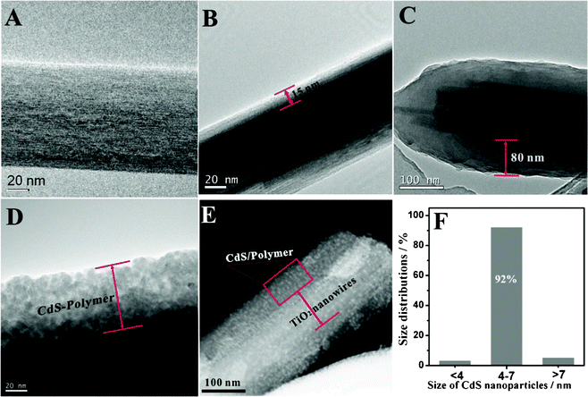 | ||
| Fig. 2 TEM images of (A) TiO2 nanowires, (B) poly(NMTE)-TiO2 nanowires, (C) P3HTA-TiO2 nanowires, (D) CdS-P3HTA-TiO2 nanowires, (E) STEM images of CdS-P3HTA-TiO2 nanowires. (F) Histogram of size distribution of CdS nanoparticles. | ||
Furthermore, the elemental composition of the CdS NC/polymer hybrid was investigated by EDX mapping images. Fig. 3 shows scanning TEM (STEM) images and several elemental mapping images; the TiO2 nanowires and polymer layers possess obvious contrast and a clear interface from the STEM measurements. These elemental mapping images conform to the STEM image. The C, S, Cd element exists in both the TiO2 nanowires and polymer layers with uniform distribution. Their mapping images show that the elemental distribution is relatively homogeneous. Because the content of the O species in the polymer layer is far less than in the TiO2 nanowires, the O mapping image shows a strong O signal in the TiO2 region; but the polymer layer on both sides of the TiO2 nanowires shows a low O content, indicated by the light-colored mapping images, which is consistent with the above analysis. The width of the Ti mapping image is smaller compared to that of others, which also provides direct proof that the polymer layers are wrapped around the TiO2 nanowires.
 | ||
| Fig. 3 STEM images of CdS nanocrystals-P3HTA-TiO2 nanowires and the corresponding EDX mapping images of the C, O, Ti, S and Cd, respectively. | ||
The ordered p–n heterojunction could easily be prepared on perpendicularly oriented TiO2 nanotubes by the same procedure. The apparent nanoporous morphology of TiO2 nanotubes is clear from the FESEM measurement, as shown in Fig. 4A. The pore size is about 100 nm and the tube wall exhibits a smooth topography, as shown in Fig. 4D. When P3THA brushes were prepared on TiO2 nanotubes, the tube end was almost covered by precipitate, which blocked the tube, as represented in Fig. 4B. From the cross sectional view in Fig. 4E, the polymer layers are covering the tube walls, which makes the tube profile unclear. After the in situ loading of CdS nanocrystals in Fig. 4C, small nanoparticles appeared on the TiO2 nanotube surface. As shown in the cross-section in Fig. 4F, the CdS nanocrystals with uniform size cover the nanotubes walls.
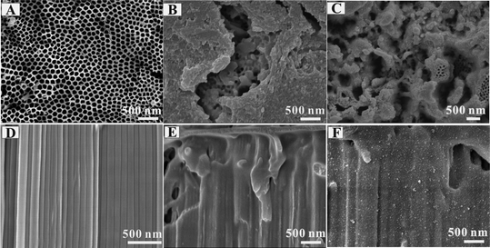 | ||
| Fig. 4 FESEM images of (A) TiO2 nanotubes, (B) poly(3THA)-TiO2 nanotubes, (C) CdS-Poly (3THA)-TiO2 nanotubes. Cross-section FESEM views of (D) TiO2 nanotubes, (E) poly(3THA)-TiO2 nanotubes, (F) CdS-poly(3THA)-TiO2 nanotubes. | ||
Successful polymer grafting and CdS nanocrystal uploading on TiO2 nanowires were further ascertained by XPS. Fig. 5A displays the XPS survey spectra of TiO2 nanowires, which are mainly composed of Ti and O, as well as a small amount of C contamination from adventitious hydrocarbon. Successful anchoring of the initiator on TiO2 nanowires is indicated by the presence of N signals, which are not detected for TiO2 nanowires (Fig. S2, ESI†). The surface chemical composition data of these surfaces are summarized in Table 1, ESI.† The presence of the strong S (2p) peak and S (2s) peak in Fig. 2A (c) confirms that P(NMTE) has been successfully grafted onto TiO2 nanowires. After the oxidation polymerization of 3-thiopheneacetic acid, the S (2p, 2s) peaks still exist, and the S atomic concentration can rise to 5.27% from 3.05% in Table 1 due to more thiophene units in the polymers. When Cd2+ was immobilized onto the polymer chains via cation exchange, the Cd 3d peaks appear at binding energies of 405.4 eV and 412.2 eV (Fig. S2†). The formation of CdS nanocrystals is verified by the signals of the S (2p) peak at binding energies of 162.6 and 161.6 eV, as shown in Fig. 5A (d). Similarly, after poly(3-hexylthiophene) is grafted onto the TiO2 nanowires, the S (2p) peak is also evident. Interestingly, from Table 1, during self-assembly of the initiator on the TiO2 nanowires, ROMP, oxidation polymerization and CdS NC loading on the TiO2 nanowires, the Ti signal was decreasing continuously, and while the P3THA polymers were being grafted on and the CdS NCs being formed, the Ti signal was negligible, which reveals that high density, thick polymers have been grafted onto the TiO2 nanowires that block detection of the Ti signal.
 | ||
| Fig. 5 (A) XPS survey spectra of (a) TiO2 nanowires, (b) poly(NMTE)-TiO2 nanowires, (c) P3THA-TiO2 nanowires, (d) CdS-P3THA-TiO2 nanowires, (e) P3TH-TiO2 nanowires. (B) TGA traces of (a) TiO2 nanowires, (b) TiO2 nanowires – initiator modified, (c) poly(NMTE)-TiO2 nanowires, (d) Cd-P3THA-TiO2 nanowires, (e) CdS-P3THA-TiO2 nanowires, (f) P3HT-TiO2 nanowires. (C) UV-Vis spectra of TiO2 nanowires (a), P3THA-TiO2 nanowires (b), CdS-P3THA-TiO2 nanowires (c). (D) Current density vs. voltage characteristics of TiO2 nanowires (a), P3THA-TiO2 nanowires (b), CdS-P3THA-TiO2 nanowires (c). | ||
TGA was carried out to evaluate the change of the organic portion during polymer grafting and CdS NC loading in Fig. 5B. TGA of TiO2 nanowires measured a 10.58% weight loss between 100 and 600 °C. Upon modification of the ROMP initiator, the composite was found to have 12.89% weight loss, so 2.31 wt% of the weight loss was from the initiator. After the ROMP of NMTE monomers, a relatively thin polymer film was coated on the TiO2 surface with a weight loss of 21.65%, as illustrated in Fig. 5B (c). When oxidation polymerization and the immobilization of Cd2+ ions onto polymer chains were performed, the TGA curve in Fig. 5B (d) shows an overall weight loss of 45.40%. After CdS NC formation, the overall weight loss decreases to 24.12%, due to the formation of high density CdS nanoparticles (Fig. 5B (e)). The P3HT grafting TiO2 nanowires shows an overall weight loss of 55.58%, corresponding to the thick polymers.
The photo absorption properties of the resulting hybrid nanocomposites were explored by UV-Vis measurement in chlorobenzene. The TiO2 nanowires show no photoresponse in the visible region, as shown in Fig. 5C (a). After grafting P3THA, with its large thiophene skeleton conjugated structure, onto the TiO2 nanowires, as shown in Fig. 5C (b), the spectral absorption of P3THA grafted TiO2 nanowires extended to the visible light region; the absorption peak appears at 405 nm and the absorption is evident before 500 nm, which corresponds to the energy band gap of polythiophene derivatives.41 The side chains, substituent groups and regularity of the conductive polymers have a great influence on the energy band gap,3 so the energy band gap can be altered from 2.33 to 1.90 eV.42 When the CdS NCs are loaded, the absorption peak of the hybrid nanocomposites moves to 450 nm and the absorption is shifted to 600 nm. CdS materials with an energy band gap of 2.25 eV can extend the absorption to a maximum of 550 nm.43 After coupling of the CdS nanocrystals to conductive polymers, the absorption can be extended to 600 nm, implying improved charge transfer between P3THA and CdS NCs, probably due to the intimate contact between these two constituents. Fig. 5D shows current density versus voltage in 0.1 M Na2S under 150 mW cm−2 illumination. The open circuit voltage (Voc) and short current density (Isc) of TiO2 nanowires were 0.55V and 0.067 mA cm−2, respectively, as shown in Fig. 5D (a). After the conductive polymers are grafted onto the TiO2 nanowires, Voc and Isc can reach 0.68 V and 0.090 mA cm−2, which could be attributed to the conductive polymers, which possess visible light harvesting ability. The CdS nanocrystal/polymer hybrids produced an increased Voc and Isc with 0.84 V and 0.137 mA cm−2, compared to polymer/TiO2 materials, which revealed that the ordered p–n heterojunction can be used as a promising building block for harvesting visible light.
4. Conclusions
In conclusion, surface initiated polymerization and oxidation polymerization were exploited to produce chemically bonded p–n heterojunctions and create ordered nanocrystal/conjugated polymer hybrid nanocomposites with a well-defined interface via a step-by-step strategy on the nanoscale. It allows conducting polymer brushes to tailor the size and dispersion of nanocrystals in order to further tune the photo properties of these hybrid materials. More importantly, the nanocrystals tightly wrapped the polymer chains, thereby affording direct interfacial contact, which is expected to greatly improve the photoelectric performance, enabling excellent charge separation and transfer with minimal carrier recombination; so high photo conversion efficiency is expected in this nano-architecture. Further studies to the structural engineering of the conjugated polymers and rational nanocrystals or nanocrystal combination design with tunable size and shape control are of utmost importance for the further development of organic/inorganic hybrid solar cells.Acknowledgements
This work was supported by NSFC (20973188, 21125316) and the “Hundred Talents Program” of Chinese Academy of Sciences.References
- Y. Zai, Y. Han, K Lu, Y. J. Zhang and Z. X. Wei, RSC Adv., 2012, 2, 338–343 RSC.
- C. R. McNeill, Energy Environ. Sci., 2012, 5, 5653–5667 CAS.
- H. Zhou, L. Yang and W. You, Macromolecules, 2012, 45, 607–632 CrossRef CAS.
- A. J. Moulé, L. Chang, C. Thambidurai, R. Vidu and P. Stroeve, J. Mater. Chem., 2012, 22, 2351–2368 RSC.
- F. He and L. Yu, J. Phys. Chem. Lett., 2011, 2, 3102–3113 CrossRef CAS.
- F. C. Krebs, T. Tromholt and M. Jorgensen, Nanoscale, 2010, 2, 873–886 RSC.
- J. E. Slota, X. He and W. T. S. Huck, Nano Today, 2010, 5, 231–242 CrossRef CAS.
- Y. Liang, D. Feng, Y. Wu, S.-T. Tsai, G. Li, C. Ray and L. Yu, J. Am. Chem. Soc., 2009, 131, 7792–7799 CrossRef CAS.
- M. Brinkmann, D. Aldakov and F. Chandezon, Adv. Mater., 2007, 19, 3819–3823 CrossRef CAS.
- R. Po, M. Maggini and N. Camaioni, J. Phys. Chem. C, 2010, 114, 695–706 CAS.
- J. Y. Kim, K. Lee, N. E. Coates, D. Moses, T. Q. Nguyen, M. Dante and A. J. Heeger, Science, 2007, 317, 222–225 CrossRef CAS.
- L.-M. Chen, Z. Hong, G. Li and Y. Yang, Adv. Mater., 2009, 21, 1434–1449 CrossRef CAS.
- G. K. Mor, S. Kim, M. Paulose, O. K. Varghese, K. Shankar, J. Basham and C. A. Grimes, Nano Lett., 2009, 9, 4250–4257 CrossRef CAS.
- K. Takamizu and K. Nomura, J. Am. Chem. Soc., 2012, 134, 7892–7895 CrossRef CAS.
- Y. Bai, J. Zhang, D. Zhou, Y. Wang, M. Zhang and P. Wang, J. Am. Chem. Soc., 2011, 133, 11442–11445 CrossRef CAS.
- D. Zhou, Q. Yu, N. Cai, Y. Bai, Y. Wang and P. Wang, Energy Environ. Sci., 2011, 2030–2034 CAS.
- X. Shen, B. Sun, F. Yan, J. Zhao, F. Zhang, S. Wang, X. Zhu and S. Lee, ACS Nano, 2010, 4, 5869–5876 CrossRef CAS.
- X. Shen, B. Sun, D. Liu and S. T. Lee, J. Am. Chem. Soc., 2011, 133, 19408–19415 CrossRef CAS.
- P. V. Kamat, J. Phys. Chem. C, 2008, 112, 18737–18753 CAS.
- A. Kongkanand, K. Tvrdy, K. Takechi, M. Kuno and P. V. Kamat, J. Am. Chem. Soc., 2008, 130, 4007–4015 CrossRef CAS.
- W. U. Huynh, J. J. Dittmer and A. P. Alivisatos, Science, 2002, 295, 2425–2427 CrossRef CAS.
- J. Bouclé, S. Chyla, M. S. P. Shaffer, J. R. Durrant, D. D. C. Bradley and J. Nelson, Adv. Funct. Mater., 2008, 18, 622–633 CrossRef.
- M. D. Goodman, J. Xu, J. Wang and Z. Lin, Chem. Mater., 2009, 21, 934–938 CrossRef CAS.
- Z. Lin, Chem.–Eur. J., 2008, 14, 6294–6301 CrossRef CAS.
- J. Albero, Y. Zhou, M. Eck, F. Rauscher, P. Niyamakom, I. Dumsch, S. Allard, U. Scherf, M. Krüger and E. Palomares, Chem. Sci., 2011, 2, 2396–2401 RSC.
- J. Xu, J. Hu, X. Liu, X. Qiu and Z. Wei, Macromol. Rapid Commun., 2009, 30, 1419–1423 CrossRef CAS.
- A. J. Moulé and K. Meerholz, Adv. Mater., 2008, 20, 240–245 CrossRef.
- Y.-Y. Lin, T.-H. Chu, S.-S. Li, C.-H. Chuang, C.-H. Chang, W.-F. Su, C.-P. Chang, M.-W. Chu and C.-W. Chen, J. Am. Chem. Soc., 2009, 131, 3644–3649 CrossRef CAS.
- L. Zhao, X. Pang, R. Adhikary, J. W. Petrich and Z. Lin, Angew. Chem., Int. Ed., 2011, 50, 3958–3962 CrossRef CAS.
- L. Zhao, X. Pang, R. Adhikary, J. W. Petrich, M. Jeffries-EL and Z. Lin, Adv. Mater., 2011, 23, 2844–2849 CrossRef CAS.
- J. Qian, Q. S. Liu, G. Li, K. J. Jiang, L. M. Yang and Y. Song, Chem. Commun., 2011, 47, 6461–6463 RSC.
- N. Balis, V. Dracopoulos, E. Stathatos, N. Boukos and P. Lianos, J. Phys. Chem. C, 2011, 115, 10911–10916 CAS.
- H.-C. Liao, C.-C. Lin, Y.-W. Chen, T.-C. Liu and S.-Y. Chen, J. Mater. Chem., 2010, 20, 5429–5435 RSC.
- V. Senkovskyy, R. Tkachov, T. Beryozkina, H. Komber, U. Oertel, M. Horecha, V. Bocharova, M. Stamm, S. A. Gevorgyan, F. C. Krebs and A. Kiriy, J. Am. Chem. Soc., 2009, 131, 16445–16453 CrossRef CAS.
- D. Wang, Q. Ye, B. Yu and F. Zhou, J. Mater. Chem., 2010, 20, 6910–6915 RSC.
- A. M. Jonas, K. Glinel, R. Oren, B. Nysten and W. T. S. Huck, Macromolecules, 2007, 40, 4403–4405 CrossRef CAS.
- X. Zhou, X. Liu, Z. Xie and Z. Zheng, Nanoscale, 2011, 3, 4929–4939 RSC.
- T. Xu, M. Yan, J. D. Hoefelmeyer and Q. Qiao, RSC Adv., 2012, 2, 854–862 RSC.
- J. Yan, Q. Ye and F. Zhou, RSC Adv., 2012, 2, 3978–3985 RSC.
- O. Azzaroni, A. A. Brown, N. Cheng, A. Wei, A. M. Jonas and W. T. S. Huck, J. Mater. Chem., 2007, 17, 3433–3439 RSC.
- R. Kroon, M. Lenes, J. C. Hummelen, P. W. M. Blom and B. de Boer, Polym. Rev., 2008, 48, 531–582 CrossRef CAS.
- A. Dkhissi, F. Ouhib, A. Chaalane, R. C. Hiorns, C. Dagron-Lartigau, P. Iratcabal, J. Desbrieres and C. Pouchan, Phys. Chem. Chem. Phys., 2012, 14, 5613–5619 RSC.
- C. X. Guo, H. B. Yang, Z. M. Sheng, Z. S. Lu, Q. L. Song and C. M. Li, Angew. Chem., Int. Ed., 2010, 49, 3014–3017 CrossRef CAS.
Footnote |
| † Electronic Supplementary Information (ESI) available. See DOI: 10.1039/c2ra21546b |
| This journal is © The Royal Society of Chemistry 2013 |