Tailoring surface plasmons of high-density gold nanostar assemblies on metal films for surface-enhanced Raman spectroscopy†
Jiwon
Lee‡
a,
Bo
Hua‡
b,
Seungyoung
Park
a,
Minjeong
Ha
a,
Youngsu
Lee
a,
Zhiyong
Fan
*b and
Hyunhyub
Ko
*a
aSchool of Energy and Chemical Engineering, Ulsan National Institute Science and Technology (UNIST), Ulsan, Republic of Korea. E-mail: hyunhko@unist.ac.kr
bDepartment of Electronic & Computer Engineering, Hong Kong University of Science & Technology (HKUST), Hong Kong SAR, China. E-mail: eezfan@ust.hk
First published on 28th October 2013
Abstract
Plasmonic systems based on metal nanoparticles on a metal film have generated great interest for surface-enhanced Raman spectroscopy (SERS) chemical sensors. In this study, we describe the fabrication of ultrasensitive SERS substrates based on high-density gold nanostar assemblies on silver films with tailored surface plasmons, where multiple field enhancements from particle–film and interparticle plasmon couplings and lightening rod effects of sharp tips of nanostars contribute to the enormous Raman enhancements. We show that the interplay between interparticle and particle–film plasmon couplings of high-density gold nanostars (GNSs) on metal and dielectric films as a function of interparticle separation can be tailored to provide maximum SERS effects. We observe that the SERS enhancement factor (EF) of GNSs on a metal film as a function of interparticle separation follows a broken power law function, where the EF increases with the interparticle separation for the strong interparticle coupling range below an interparticle separation of ∼0.8 times the GNS size, but decreases for the weak interparticle coupling range (for an interparticle separation of >0.8 times the GNS size). Finally, we demonstrate the use of tailored plasmonic substrates as ultrasensitive SERS chemical sensors with an attomole level of detection capability of 2,4-dinitrotoluene, a model compound of nitroaromatic explosives.
Introduction
The collective oscillation of electrons of noble metals by incident light leads to enhanced electromagnetic fields, confined to propagate along metal–dielectric interfaces in the form of surface plasmon polaritons (SPPs), or localized to surface roughness features or nanoparticles as localized surface plasmons (LSPs).1,2 The enhanced electromagnetic fields associated with metal nanostructures are of great scientific interest, and essential for a wide range of applications, including surface-enhanced spectroscopies,3–5 molecular sensors,3,6–10 imaging,11–13 light harvesting,14,15 waveguides,16,17 and optical circuits.16,18 In particular, the enhanced fields are widely utilized in surface-enhanced Raman scattering (SERS),7,19–24 where Raman scattering of molecules is enhanced by many orders of magnitude when the molecules are within the localized region with greatly amplified electric fields (E-fields), or so-called “hot spots”. The hot spots exist in the subnanometer gaps between nanoparticles and near the sharp corners and asperities of the metal nanostructure. A wide variety of approaches have been used to provide SERS hot spots, such as fractal aggregation of noble metal nanoparticles,25,26 regular nanoparticle assemblies,27,28 and metal films over nanospheres;29,30 however, the precise control and reproducible formation of nanometer-scale gap distances between nanoparticles remain a challenge for SERS substrate fabrication.Recently, plasmonic systems consisting of metal nanoparticles separated from metal films by nanometer scale gaps have attracted great attention as SERS substrates, because the precise gap regions between metal nanoparticles and films can provide reproducible hot spots with large SERS enhancements.31–37 Similar to the interparticle couplings between LSPs of metal nanoparticles, the LSPs of metal nanoparticles can couple with their own image charges in the metal films or the propagating SPPs at the surface of metal films, rendering the formation of hot spots between the nanoparticles and films.38,39 Theoretical and experimental studies have shown that the plasmonic properties of particle-on-film systems are strongly dependent on the gap distances between nanoparticles and films, the nanoparticle shapes and sizes, and the dielectric properties of both substrates and their environments.40–43 Plasmonic systems, consisting of a single metal nanoparticle or a nanoparticle pair on a metal film, have been investigated extensively, resulting in a good understanding of the plasmonic coupling of the LSP of individual nanoparticles with its image charges or SPP modes on the metal film.41–46 However, few studies have been performed on plasmonic systems consisting of high-density metal nanoparticle assemblies on metal films,47–49 where the strong interparticle couplings in high-density nanoparticle assemblies are expected to affect the nanoparticle–film plasmon couplings.
For the design of highly-sensitive SERS substrates based on high-density metal nanoparticle assemblies on metal films, it is critical to understand the effects of nanoparticle surface densities on the interparticle and the particle–film plasmon couplings and the resulting ensemble-averaged E-field enhancements. Here we report on our investigation of the plasmonic properties of high-density gold nanostar (GNS) assemblies arranged on various metals (silver and gold) and dielectric (silicon and glass) substrates. In particular, by analyzing the finite-difference time-domain (FDTD) calculation of E-fields and the experimental SERS intensities, we observed that the E-fields from particle–film plasmon couplings were strongly affected by interparticle couplings, which depended on the GNS surface densities (or interparticle gap separations). Based on the understanding of the effects of GNS surface density on the interplay between interparticle and particle–film couplings, we fabricated optimally designed SERS substrates with tailored surface plasmons that can detect target molecules on the scale of an attomole.
Result and discussion
Fig. 1(a) shows a scanning electron microscopy (SEM) image of high density GNS assemblies on a metal film, which provide multiple E-field enhancements from interparticle (GNS–GNS) and particle–film (GNS–film) couplings, supported by the propagating SPPs on the metal film (Fig. 1(b)). Here, the excitation of SPPs on metal films by the incident light was enabled by the existence of GNSs. The GNSs acted as nanoantenna receivers that couple the incident light into SPP modes in the underlying metal films.47,50 The inset in Fig. 1(a) shows a transmission electron microscopy (TEM) image of GNSs (core diameter: 57 ± 9 nm; branch length: 11 ± 3 nm; bottom diameter of the branch: 18 ± 5 nm; and tip diameter of the branch: 9 ± 3 nm). Ultraviolet-visible (UV-vis) absorption measurements confirmed a LSP resonance (LSPR) peak at ∼640 nm (Fig. S1†), which is attributed to the surface plasmons of the branched tips.51 For the assembly of high-density GNSs on the substrates, we utilized electrostatic interactions between the negatively-charged sodium citrate added to the GNS solution and the positively-charged poly(diallyl dimethylammonium) (PDDA) layer on the substrates (Fig. 1(c)).52,53 This assembly process formed uniform high-density GNS assemblies that were separated from the metal films by a ∼1 nm thick PDDA layer (Fig. S2†).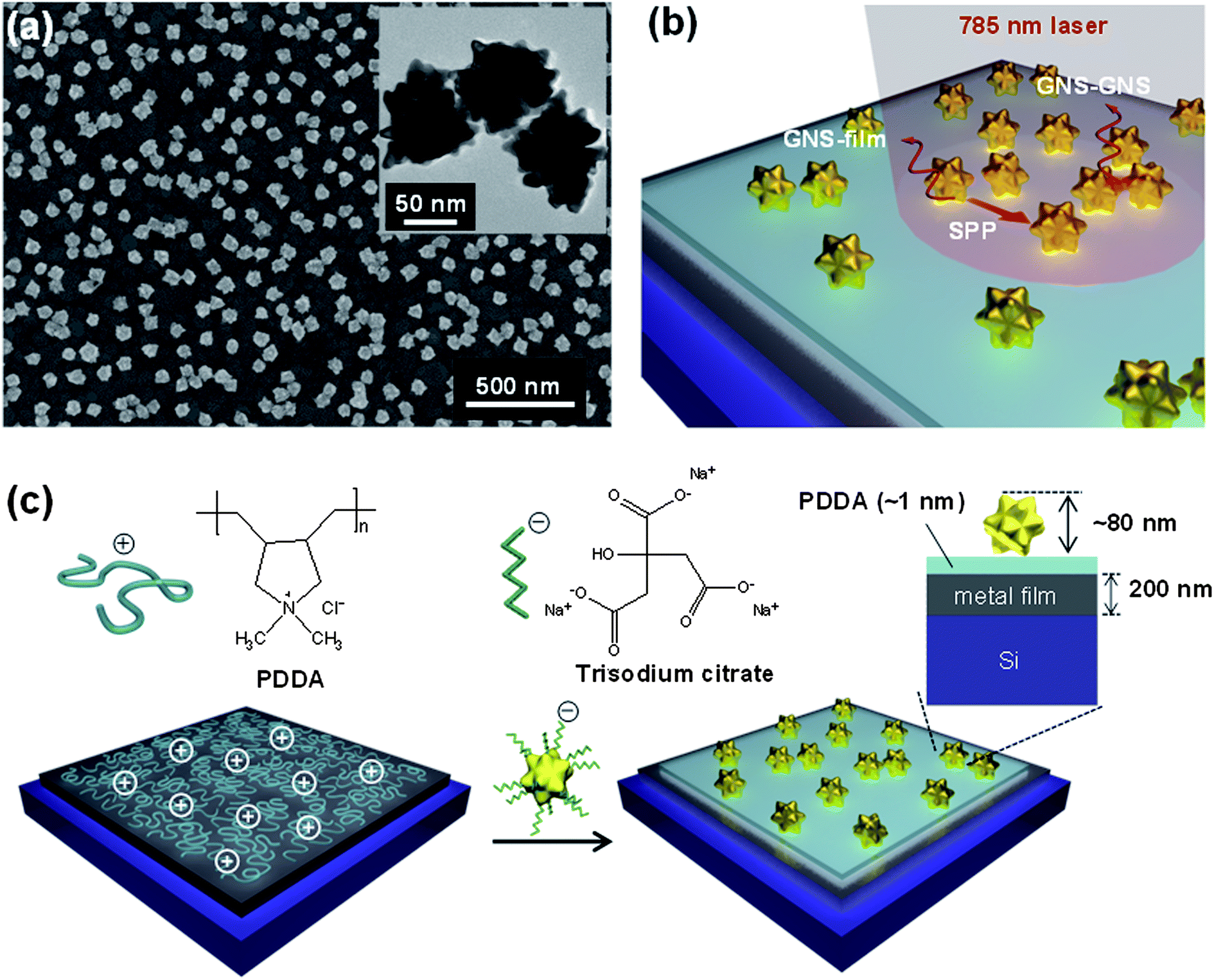 | ||
| Fig. 1 Formation of high-density GNS assemblies on metal films. (a) An SEM image of high-density GNS assemblies on a metal film. The inset shows a TEM image of GNSs with sharp tips. (b) Schematic representation of field enhancements on the high-density GNS assemblies on a metal film showing the GNS–film and GNS–GNS plasmon couplings, in combination with the propagating SPP modes on the metal film. (c) Schematic procedure of the electrostatic assembly of high-density GNSs on metal films via the electrostatic interaction between negatively charged sodium citrate additives on the GNS assemblies and the positively charged PDDA coating on the metal film. | ||
To investigate the effects of different substrates on the SERS properties of GNS assemblies, we used 200 nm thick Au and Ag films on Si substrates, as well as Si and glass substrates. Fig. 2(a) shows the Raman spectra of 0.1% benzenethiol molecules adsorbed on SERS substrates consisting of GNS assemblies on Au, Ag, Si, and glass surfaces with a PDDA layer in between (SEM images in Fig. S3†). The intensity of the Raman spectra was strongest for GNS assemblies on Ag films, followed by Au, Si, and glass substrates. In particular, we noted that the SERS EF increased from 2.7 × 10⁵ for GNS assemblies on the glass surface to 4.4 × 10⁷ for GNS assemblies on the Ag surface, which is a 160-fold increase (Fig. 2(b)). This significant increase in the SERS EF indicates the critical role of plasmon couplings between GNSs and metal films in addition to the interparticle plasmon couplings in high-density GNS assemblies on metal films. The LSPs of GNS assemblies hybridize with the propagating SPPs on the noble metal (Au, Ag) films and also interact with their image charges in the metal films,38,39 resulting in a strong enhancement of the E-fields in the particle–film gap region.32,35,37,43 In contrast, for GNS assemblies on dielectric substrates (silicon and glass), there are only image charge contributions, with no evidence of the effects of hybridization between the LSPs and SPPs; this is attributed to the absence of SPP modes on the surface of the dielectric substrates,40,54 resulting in a relatively weak SERS enhancement (Fig. 2(a) and (b)). The difference in SERS EFs on metal and dielectric substrates agreed well qualitatively with the FDTD simulations of the E-field intensity for GNSs assembled on different substrates (Fig. S4†).
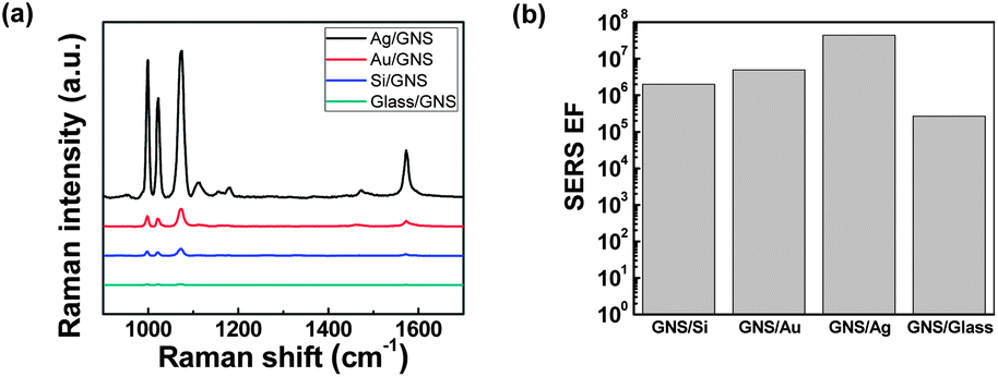 | ||
| Fig. 2 Comparison of surface-enhanced Raman spectroscopy (SERS) intensities of high-density GNS assemblies assembled on different metal and dielectric substrates. (a) SERS spectra of 0.1% benzenethiol molecules adsorbed on high-density GNS assemblies on metal (Ag, Au) and dielectric (Si, glass) substrates. (b) SERS enhancement factors of high-density GNS assemblies on Ag, Au, Si, and glass substrates. | ||
We also noted that the SERS EF for the Ag surface was about ∼9× stronger than that for the Au surface (Fig. 2(b)), which can be explained by the difference in optical loss between the Au and Ag surfaces. The SPP modes excited in the metal film have been known to enhance interactions between the LSPs of metal nanoparticles on a metal film.43 Because Ag has a lower optical loss and longer SPP propagation length than Au,55 Ag films can support stronger interparticle couplings in GNS assemblies and thus provide larger SERS EFs. The difference in the SERS EF between the non-conducting Si and glass substrates is attributed to the difference in the permittivity of the substrates. The substrates with a higher permittivity (ε) provide stronger image charges and thus larger interactions with the LSPs of metal nanoparticles.40,56 Therefore, Si substrates (ε ∼ 11.76 at the frequency of 0.5 MHz)57 exhibited a larger SERS EF than that of glass substrates (ε ∼ 4.6 at the frequency of 94 GHz).58
To understand the behavior of interparticle and particle–film plasmon couplings with different interparticle separations for GNSs on metal and dielectric substrates, FDTD simulations were carried out to analyze the E-field enhancements for the interparticle and particle–film gap regions. Fig. 3(a) and (b) show the FDTD simulation results for the E-field distribution of GNS assemblies on Ag and glass substrates with an interparticle tip-to-tip separation of 10 nm. Detailed inspection of the local E-fields in the gap regions clearly showed distinct field intensities at the interparticle and particle–film gaps (Fig. 3(c) and (d)). Fig. 3(c) indicates that the local fields at the gap between the GNS tip and the Ag film were significantly stronger than those between the GNS tips. On the other hand, for GNSs on a glass substrate, the local fields between the tips were similar to those between the GNS tip and the glass surface (Fig. 3(d)). Note that hot spots with strongly-enhanced E-fields were located directly between the tip and the film for the GNS–Ag gap, which was different from the hot spots located near the end of the tip for the GNS–glass gap. Additionally, for GNSs on a Ag film, the E-field from interparticle coupling was ∼30% stronger than that for GNSs on a glass substrate. All of these observations imply that the plasmon coupling behaviors are different for GNS–Ag and GNS–glass systems.
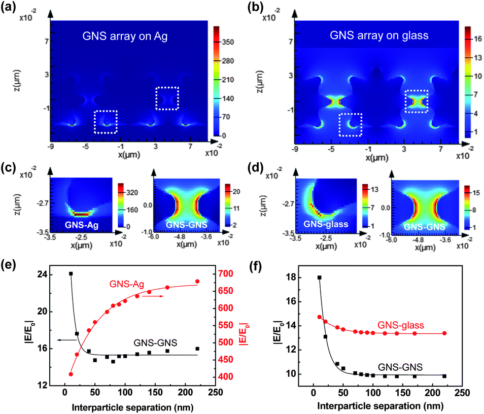 | ||
| Fig. 3 FDTD simulations of E-fields on GNS assemblies on Ag and glass substrates. E-field distribution of GNSs on (a) Ag and (b) glass substrates with an interparticle tip-to-tip distance of 10 nm. (c) Local E-fields at the GNS–Ag film gap and the GNS–GNS gap for a GNS assembly on a Ag film. (d) Local E-fields at the GNS–glass surface gap and the GNS–GNS gap for a GNS assembly on a glass substrate. Local E-field enhancement from particle–film and interparticle plasmon couplings as a function of interparticle separation for (e) GNS assemblies on Ag films and (f) GNS assemblies on glass substrates. The solid curves represent data fitting of the exponential decay function y = y0 + ae−x/l. | ||
To shed light on plasmon coupling behaviors that depend on interparticle separations, the local (GNS–Ag, GNS–GNS) E-field enhancements (|E/E0|) as a function of interparticle separation were analyzed for GNS assemblies on Ag and glass substrates (Fig. 3(e) and (f)). For GNS assemblies on Ag films, the field enhancement from GNS–GNS coupling decayed exponentially as the interparticle separation (D) increased, which is typically observed for near-field interactions in nanoparticle assemblies.59,60 The field enhancement was well fit with the exponential decay curve y = a × exp(−x/l) + y0, resulting in an amplitude of a = 33.1 and a decay length of l = 7.5. Here, the amplitude (a) tells us the magnitude of the E-field dependence on the interparticle gap distance and the decay length (l) tells us the exponential damping length of the E-field intensity. However, the field enhancement from GNS–Ag film coupling exhibited an inverse exponential decay curve as a function of interparticle separation (a = −310.6, l = 51.9). This inverse exponential decay behavior can be explained by the competition between the GNS–GNS and GNS–Ag film couplings. For small interparticle separations, the strong GNS–GNS coupling leads to the screening of particle–film plasmon couplings, in particular the hybridization between the LSP and SPP modes. The opposite behavior happens for the large interparticle separations. In contrast, the field enhancements from the GNS–Ag film couplings were significantly larger (16–42× larger) than those from GNS–GNS couplings, indicating the significance of GNS–Ag film couplings in the overall E-field enhancements for systems with GNS assemblies on Ag films. For GNS assemblies on glass substrates, the field enhancements from both GNS–GNS and GNS–glass couplings exhibited exponential decay with interparticle separation (Fig. 3(f)). The dependence of the field enhancement on the interparticle separation was stronger for GNS–GNS coupling, which was indicated by the larger amplitude (a = 18.7) for GNS–GNS coupling compared with that for GNS–glass coupling (a = 2.0). It is also worth noting that the field enhancement from interparticle couplings on the Ag film showed 30–60% larger values than those on a glass substrate; this was attributed to the enhanced interparticle plasmon couplings on the Ag film compared with those on the glass substrate due to the propagating SPP modes in the Ag film.47
The above FDTD simulations of field enhancements for GNS assemblies on Ag and glass substrates indicated that the E-field enhancement was predominantly from particle–film couplings for GNS assemblies on Ag films, whereas the system of GNS assemblies on glass substrates had E-field contributions from both weak particle–film and interparticle plasmon couplings. As reported previously, both the resonant wavelength shift and the field enhancement exhibit a universal exponential or power law dependence on the interparticle separation for metal nanoparticle dimers on dielectric substrates.60,61 For metal nanoparticles on metal substrates, previous research has shown that the power law function of both the resonant wavelength shift and field enhancement is dependent on the particle–film separation.43 However, it is still unclear whether there is a general law governing the relationship between the overall SERS enhancements and the interparticle separations for GNS assemblies on metal substrates.
To investigate this relationship further, we compared FDTD simulation results with the experimental results of the SERS intensity as a function of interparticle separation. For this purpose, we prepared different surface densities of GNSs on Ag and glass substrates (Fig. S5†) and measured the SERS intensities of benzenethiol molecules (Fig. S6†). For the analysis of SERS intensity as a function of interparticle separation, we converted the experimental GNS surface density into interparticle separation by approximating the randomly distributed GNS assemblies as hexagonal packed GNS assemblies. Additionally, to compare the experimental SERS intensity with the simulated EF, we used a GNS density-normalized EF (EFN), which can be approximated as EFN = (4|E/E0|GNS–film4 + (|E/E0|GNS–GNS4)) × (GNS surface density), where E and E0 are the local and incident electric fields, respectively.62 A detailed description of EFN is given in the ESI.†Fig. 4 shows the simulated EFN and the experimental SERS intensity as a function of the interparticle separation on Ag and glass substrates.
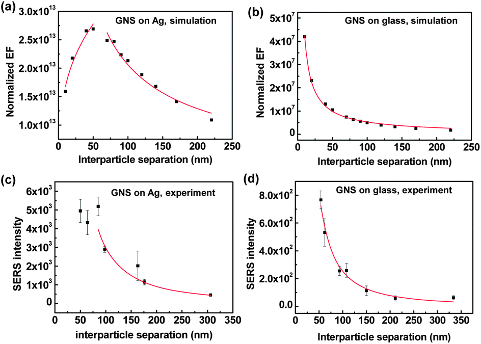 | ||
| Fig. 4 Normalized enhancement factor (EF) for the GNS assemblies on the (a) Ag films and (b) glass substrates as a function of the interparticle separation. Measured SERS intensity as a function of interparticle separation for GNS assemblies on the (c) Ag films and (d) glass substrates. The solid curves represent data fitting using the power law function y = axb. | ||
Fig. 4(a) and (b) show that the normalized EF as a function of interparticle separation was well fit by the power law (y = axb), where a and b are fitting parameters. We also determined that the normalized EF of the GNS assemblies on Ag films, as a function of interparticle separation, followed a broken power law function or a combined power law distribution (Fig. 4(a)). At first, the normalized EF increased as the interparticle separation increased, following a power law function with an index (b) of 0.31 ± 0.05 for interparticle separation below ∼60 nm; however, the normalized EF decreased with b = −0.68 ± 0.05 for interparticle separation over ∼60 nm. This behavior can be explained by the interplay between interparticle and particle–film plasmon couplings, where the particle–film plasmon couplings become weak when there is strong interference from interparticle couplings. Therefore, when the interparticle separation was below ∼60 nm, i.e., below ∼0.8 times the GNS size (80 nm) (i.e., the strong interparticle coupling range), the E-field from particle–film couplings increased exponentially as the interparticle separation increased or as the interparticle coupling decreased exponentially (Fig. 3(e)). When the interparticle separation was over ∼60 nm (i.e., the weak interparticle coupling range), the increase in the E-field from particle–film couplings began to saturate as the interparticle separation increased. Because the particle–film couplings dominate in the weak interparticle coupling range, the normalized EF strongly depended on the number of hot spots from particle–film couplings, which in turn depended on the GNS assembly surface density. Therefore, the normalized EF decreased with an increase in the interparticle separation or decrease in the GNS surface density for an interparticle separation over ∼60 nm.
For GNS assemblies on glass substrates, the EF decreased as the interparticle separation increased, as described by the single power law index of b = −0.90 ± 0.02, in agreement with previous reports (Fig. 4(b)).61 The smaller value of the power law index (b = −0.68) for the GNS assemblies on Ag films, as compared to that on glass substrates (b = −0.90), indicated that the SERS enhancement was less sensitive to interparticle separation. To compare the simulation results with the experimental results, Fig. 4(c) and (d) show the measured SERS intensity as a function of interparticle separation. The experimental SERS intensity for GNSs on Ag films exhibited a value of b = −1.71 for interparticle separation over ∼80 nm and b = −1.70 for GNSs on glass substrates. The difference in the power law exponents for the simulated EF and experimental SERS intensity is attributed to the regular GNS assemblies used in the simulated EF as opposed to the random distribution of GNSs in the experimental SERS results, which resulted in the dispersion of interparticle separations and occasional nanostar aggregations. It is worth noting that the trends in simulation results match quite well with the experimental results although the simulation work is based on regular GNS assemblies, where the long-range effects could affect the trends. However, in our study, the long-range effects from the regular GNS assembly in the simulation results can be considered to be minimal since the periodicity is far below the excitation wavelength.
Because the GNS surface density can affect the interplay between the interparticle and particle–film plasmon couplings, the density-controlled, optimally designed SERS substrates could be advantageous for trace-level detection of analytes. Fig. 5(a) shows the Raman spectra of benzenethiol (concentrations varying from 10 nM to 1 aM) adsorbed on optimized SERS substrates (GNS assemblies on Ag films with a GNS surface density of ∼43 GNSs per μm2). Optimization of the SERS substrates with maximum SERS effects was enabled by controlling the GNS surface density. The Raman spectra of benzenethiol with C–H out-of-plane bending (998 cm−1) and C–C symmetric stretching (1021, 1071 cm−1) were observed. Compared with the Ag/PDDA/GNS substrates without benzenethiol molecules, the Raman peak at 998 cm−1 was clearly visible down to 1 attomole (aM) with the signal-to-noise ratio over ∼6 (Fig. S7†), demonstrating the ultrasensitive detection capability of the SERS substrates based on GNS assemblies on metal films. This detection capability is not achievable with typical gold nanosphere assemblies on Ag films (Fig. S8†). The ultrasensitive detection capability of our SERS substrates is attractive for the trace level detection of explosives. Since the 2,4-dinitrotoluene (2,4-DNT) is a residue of TNT-based explosives, the detection of trace amounts of 2,4-DNT is an important requirement for the landmine detection and security checkpoints in the airport. As shown in Fig. 5(b), our SERS substrates allow the detection of 10 aM of 2,4-DNT with characteristic vibration modes of NO2 out-of-plane bending modes at 834 cm−1 and NO2 symmetric stretching modes at 1355 cm−1. The detection of DNT down to 10 aM is well below the best known detection limit of DNT (∼4 fM) based on 3D SERS substrates.63
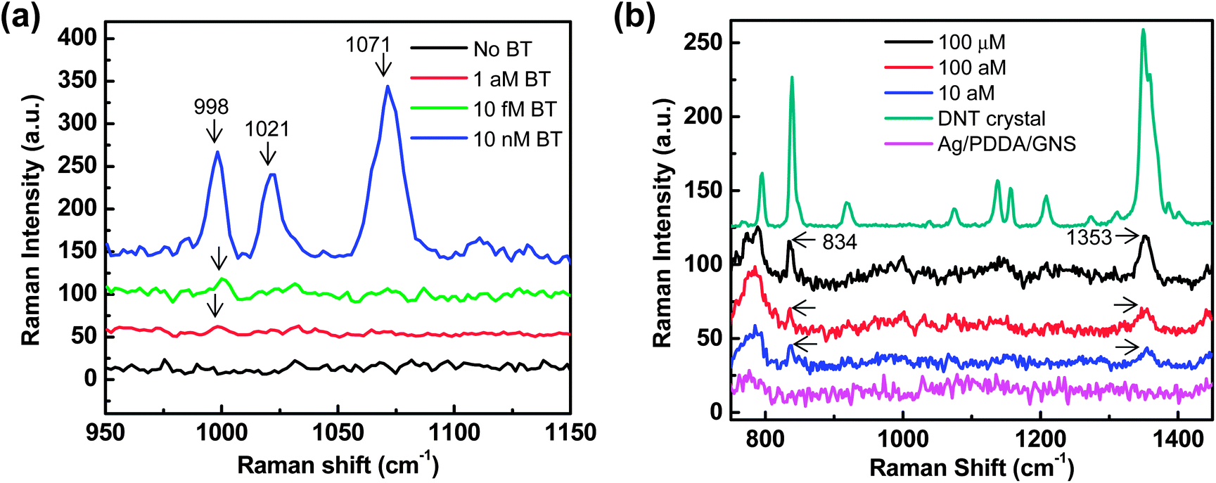 | ||
| Fig. 5 Raman measurements of trace level molecules on optimized SERS substrates (GNS assemblies on a Ag film with a GNS surface density of ∼43 GNSs per μm2) (a) Raman spectra of benzenethiol (BT, concentrations varying from 10 nM to 1 aM) showing the C–H out-of-plane bending (998 cm−1) and C–C symmetric stretching (1021, 1071 cm−1) modes of adsorbed benzenethiol molecules. (b) Raman spectra of 2,4-dinitrotoluene (DNT, concentration varying from 100 μM to 10 aM) showing NO2 out-of-plane bending at 834 cm−1 and NO2 symmetric stretching at 1355 cm−1. The DNT crystal shows a normal Raman spectrum of thick DNT solids formed on Si substrates. | ||
Conclusions
In summary, we demonstrated the fabrication of ultrasensitive SERS substrates based on high-density gold nanostar assemblies on silver films, where multiple field enhancements from particle–film and interparticle plasmon couplings and lightening rod effects of sharp tips of nanostars contribute to the enormous Raman enhancements. We also demonstrated that the interplay between interparticle and particle–film plasmon couplings of GNS assemblies on metal and dielectric films significantly affected the overall field enhancements, resulting in different power law functions of the SERS EF as a function of interparticle separation. GNS assemblies on the metal film were described by a broken power law function, where the SERS EF increased with interparticle separation for the strong interparticle coupling range. However, the SERS EF decreased as the interparticle separation increased for the weak interparticle coupling range. This study provides a platform to fabricate ultrasensitive SERS substrates via precise control of the nanoparticle surface density on metal films for maximum field enhancements, leading to the attomole detection of explosives. This approach shows great potential for a wide range of applications such as in ultrasensitive detection of target molecules in surface-enhanced spectroscopies and imaging, and in enhanced light absorption and detection using optoelectronic devices.Experimental
Synthesis of gold nanostars
Gold nanostars (GNSs) were synthesized using a seed-mediated approach, where spherical gold nanoparticles (∼18 nm in diameter) were used as seeds. Chloroauric acid was reduced on the surface of the GNSs with hydroxylamine sulfate (NH2OH, Sigma-Aldrich). The gold nanoparticle seeds were prepared by the Turkevich–Frens method,64,65 using sodium citrate as a reducing agent in an aqueous solution. Briefly, 150 mL of 0.25 mM aqueous solution of HAuCl4 was heated to the boiling point under stirring, and then 1.15 mL of 0.1 M aqueous solution of sodium citrate was added. The solution was kept under boiling conditions until a red-wine color appeared. The solution was then cooled to room temperature. The synthesis of GNSs based on Au nanoparticle seeds was carried out in a 75 mL aqueous solution with 2-[4-(2-hydroxyethyl)-1-piperazinyl] ethane-sulfonic acid (HEPES, 25 mM, pH 7.0, Sigma-Aldrich). Then, 1.6 mL of 18 nm Au seeds and 0.12 mL of NH2OH (100 mM) were added to the HEPES solution; in this case, NH2OH was used as a precision shape-directing agent.66,67 The enlargement of the Au nanoparticle seeds was achieved by first adding 5 mL of an aqueous solution of HAuCl4 (0.8 mM) dropwise; the reaction mixture was then stirred for over 5 h at 4 °C, and then the solution was stored in a refrigerator until use.Assembly of gold nanostar assemblies
For the assembly of GNS assemblies on the substrates, we used the electrostatic interaction between the negatively charged sodium citrate added into the GNS solution and the positively charged poly(diallyldimethylammonium chloride) (PDDA, 100![[thin space (1/6-em)]](https://www.rsc.org/images/entities/char_2009.gif) 000 MW, Sigma-Aldrich) layer on the substrates.32,41,53,63,68 The PDDA layer was prepared by spin-coating of a 0.2% PDDA solution, followed by rinsing with deionized (DI) water, resulting in a ∼1 nm thick layer on the substrates. To fabricate metal film-coated substrates, the gold and silver films (∼200 nm in thickness) were deposited onto Si substrates using the thermal evaporation method. The roughness values were 3.26 nm for gold and 3.74 nm for silver films (Fig. S9†). A cover slip glass (thickness: ∼1 mm) was used as the glass substrate. For the high-density assembly of GNS assemblies, the as-synthesized GNS solution was concentrated (∼15×) by centrifugation, and 38.8 mM sodium citrate solution was added to the mixture. High-density GNS assemblies could be achieved by controlling the amount of sodium citrate, where the increase in the sodium citrate concentration resulted in an increase in the GNS surface density (Fig. S10†). To vary the surface densities of GNS assemblies from low to high densities, the substrates were dipped into the GNS solution and kept there for a certain period of time until the desired surface density was achieved (Fig. S5†).
000 MW, Sigma-Aldrich) layer on the substrates.32,41,53,63,68 The PDDA layer was prepared by spin-coating of a 0.2% PDDA solution, followed by rinsing with deionized (DI) water, resulting in a ∼1 nm thick layer on the substrates. To fabricate metal film-coated substrates, the gold and silver films (∼200 nm in thickness) were deposited onto Si substrates using the thermal evaporation method. The roughness values were 3.26 nm for gold and 3.74 nm for silver films (Fig. S9†). A cover slip glass (thickness: ∼1 mm) was used as the glass substrate. For the high-density assembly of GNS assemblies, the as-synthesized GNS solution was concentrated (∼15×) by centrifugation, and 38.8 mM sodium citrate solution was added to the mixture. High-density GNS assemblies could be achieved by controlling the amount of sodium citrate, where the increase in the sodium citrate concentration resulted in an increase in the GNS surface density (Fig. S10†). To vary the surface densities of GNS assemblies from low to high densities, the substrates were dipped into the GNS solution and kept there for a certain period of time until the desired surface density was achieved (Fig. S5†).
Characterization
The synthesized Au nanospheres were characterized using UV-vis spectrophotometry (V-670, JASCO), field-emission scanning electron microscopy (FE-SEM, Nano 230, FEI), and transmission electron microscopy (TEM, JEOL). The roughness of Ag and Au films was measured by atomic force microscopy (AFM, Veeco). The thickness of PDDA was measured by AFM and spectroscopic ellipsometry (M-2000, J. A. Woollam).For the SERS measurement of analytes, SERS substrates were prepared by varying the concentration of benzenethiol (Sigma-Aldrich) solution from 100 μM to 1 aM in ethanol. The SERS substrates were immersed in the benzenethiol solution for 15 min, rinsed with ethanol, and then blown dry with nitrogen gas. For the SERS measurement of 2,4-DNT, the SERS substrates are immersed in the DNT solution in methanol with the concentration from 100 μM to 10 aM for 2 hours, rinsed in methanol, and blown dry. The Raman spectra of the analytes were collected with 785 nm laser excitation using a confocal Raman microscope (Alpha 300, WITec) and an objective lens (20×, numerical aperture = 0.4). The integration time was 0.5 s; the laser power was ∼15 mW.
Finite difference time domain method (FDTD) simulation
The E-field intensity distribution is calculated by the finite difference time domain method (Lumerical FDTD Solutions, version 8.5). The shape of nanostars built in the simulation is based on TEM pictures. A nanostar consists of a spherical core and 12 conical branches with round tips. The diameter of the spherical core is 57 nm. For conical branches, their length is about 11 nm, and the root diameter and tip diameters are 18 nm and 9 nm, respectively. The light source is a linearly polarized plane wave of 785 nm wavelength, with an incident electric field intensity of 1 V m−1. In order to make the simulation result as accurate as possible, a mesh size of 0.5 nm was used around and inside the Au nanostars. Symmetric and anti-symmetric boundaries were used in y and x directions to reduce the simulation time, considering that Au nanostars are symmetrically designed. While for the z direction, a perfectly matched layer (PML) boundary condition was used. In the FDTD simulation of the regular GNS assemblies, the GNS assemblies were arranged in the 2D hexagonal assemblies.Acknowledgements
This work was supported by the National Research Foundation of Korea (NRF-2011-0014965), Korea Institute of Science and Technology (KIST) (2E22112-11-249), and Korea Institute of Machinery & Materials (KIMM) (NK175B).Notes and references
- E. Hutter and J. H. Fendler, Adv. Mater., 2004, 16, 1685–1706 CrossRef CAS.
- S. A. Maier and H. A. Atwater, J. Appl. Phys., 2005, 98, 041301 CrossRef.
- S. Lal, S. Link and N. J. Halas, Nat. Photonics, 2007, 1, 641–648 CrossRef CAS.
- C. Genet and T. W. Ebbesen, Nature, 2007, 445, 39–46 CrossRef CAS PubMed.
- B. Peng, G. Y. Li, D. H. Li, S. Dodson, Q. Zhang, J. Zhang, Y. H. Lee, H. V. Demir, X. Y. Ling and Q. H. Xiong, ACS Nano, 2013, 7, 5993–6000 CrossRef CAS PubMed.
- M. E. Stewart, C. R. Anderton, L. B. Thompson, J. Maria, S. K. Gray, J. A. Rogers and R. G. Nuzzo, Chem. Rev., 2008, 108, 494–521 CrossRef CAS PubMed.
- K. Kneipp, H. Kneipp, I. Itzkan, R. R. Dasari and M. S. Feld, Chem. Rev., 1999, 99, 2957–2975 CrossRef CAS PubMed.
- Y. Shen, J. Zhou, T. Liu, Y. Tao, R. Jiang, M. Liu, G. Xiao, J. Zhu, Z.-K. Zhou, X. Wang, C. Jin and J. Wang, Nat. Commun., 2013, 4, 2381 Search PubMed.
- X. Xu, B. Peng, D. Li, J. Zhang, L. M. Wong, Q. Zhang, S. Wang and Q. Xiong, Nano Lett., 2011, 11, 3232–3238 CrossRef CAS PubMed.
- C. Cao, J. Zhang, X. Wen, S. L. Dodson, N. T. Dao, L. M. Wong, S. Wang, S. Li, A. T. Phan and Q. Xiong, ACS Nano, 2013, 7, 7583–7591 CrossRef CAS PubMed.
- N. Fang, H. Lee, C. Sun and X. Zhang, Science, 2005, 308, 534–537 CrossRef CAS PubMed.
- S. Kawata, Y. Inouye and P. Verma, Nat. Photonics, 2009, 3, 388–394 CrossRef CAS.
- C. J. Murphy, A. M. Gole, S. E. Hunyadi, J. W. Stone, P. N. Sisco, A. Alkilany, B. E. Kinard and P. Hankins, Chem. Commun., 2008, 544–557 RSC.
- H. A. Atwater and A. Polman, Nat. Mater., 2010, 9, 205–213 CrossRef CAS PubMed.
- J. A. Schuller, E. S. Barnard, W. S. Cai, Y. C. Jun, J. S. White and M. L. Brongersma, Nat. Mater., 2010, 9, 193–204 CrossRef CAS PubMed.
- D. K. Gramotnev and S. I. Bozhevolnyi, Nat. Photonics, 2010, 4, 83–91 CrossRef CAS.
- R. Yan, P. Pausauskie, J. Huang and P. Yang, Proc. Natl. Acad. Sci. U. S. A., 2009, 106, 21045–21050 CrossRef CAS PubMed.
- W. L. Barnes, A. Dereux and T. W. Ebbesen, Nature, 2003, 424, 824–830 CrossRef CAS PubMed.
- H. Ko, S. Singamaneni and V. V. Tsukruk, Small, 2008, 4, 1576–1599 CrossRef CAS PubMed.
- K. A. Willets and R. P. Van Duyne, Annual Reviews, Palo Alto, 2007, vol. 58, pp. 267–297 Search PubMed.
- M. Moskovits, J. Raman Spectrosc., 2005, 36, 485–496 CrossRef CAS.
- R. Kodiyath, T. A. Papadopoulos, J. Wang, Z. A. Combs, H. Li, R. J. C. Brown, J.-L. Brédas and V. V. Tsukruk, J. Phys. Chem. C, 2012, 116, 13917–13927 CAS.
- R. Kodiyath, J. Wang, Z. A. Combs, S. Chang, M. K. Gupta, K. D. Anderson, R. J. Brown and V. V. Tsukruk, Small, 2011, 7, 3452–3457 CrossRef CAS PubMed.
- R. Kodiyath, S. T. Malak, Z. A. Combs, T. Koenig, M. A. Mahmoud, M. A. El-Sayed and V. V. Tsukruk, J. Mater. Chem. A, 2013, 1, 2777–2788 CAS.
- B. Yan, A. Thubagere, W. R. Premasiri, L. D. Ziegler, L. Dal Negro and B. M. Reinhard, ACS Nano, 2009, 3, 1190–1202 CrossRef CAS PubMed.
- K. Kim, D. Shin, K. L. Kim and K. S. Shin, Phys. Chem. Chem. Phys., 2010, 12, 3747–3752 RSC.
- J. Theiss, P. Pavaskar, P. M. Echternach, R. E. Muller and S. B. Cronin, Nano Lett., 2010, 10, 2749–2754 CrossRef CAS PubMed.
- A. Chen, A. E. Deprince, III, A. Demortiere, A. Joshi-Imre, E. V. Shevchenko, S. K. Gray, U. Welp and V. K. Vlasko-Vlasov, Small, 2011, 7, 2365–2371 CrossRef CAS PubMed.
- L. A. Dick, A. D. McFarland, C. L. Haynes and R. P. Van Duyne, J. Phys. Chem. B, 2002, 106, 853–860 CrossRef CAS.
- X. Zhang, J. Zhao, A. V. Whitney, J. W. Elam and R. P. Van Duyne, J. Am. Chem. Soc., 2006, 128, 10304–10309 CrossRef CAS PubMed.
- J. D. Driskell, R. J. Lipert and M. D. Porter, J. Phys. Chem. B, 2006, 110, 17444–17451 CrossRef CAS PubMed.
- L. Rodriguez-Lorenzo, R. A. Alvarez-Puebla, I. Pastoriza-Santos, S. Mazzucco, O. Stephan, M. Kociak, L. M. Liz-Marzan and F. J. Garcia de Abajo, J. Am. Chem. Soc., 2009, 131, 4616–4618 CrossRef CAS PubMed.
- M. Rycenga, X. Xia, C. H. Moran, F. Zhou, D. Qin, Z. Y. Li and Y. Xia, Angew. Chem., 2011, 123, 5587–5591 CrossRef.
- Y. Chu, M. G. Banaee and K. B. Crozier, ACS Nano, 2010, 4, 2804–2810 CrossRef CAS PubMed.
- R. T. Hill, J. J. Mock, Y. Urzhumov, D. S. Sebba, S. J. Oldenburg, S. Y. Chen, A. A. Lazarides, A. Chilkoti and D. R. Smith, Nano Lett., 2010, 10, 4150–4154 CrossRef CAS PubMed.
- G. Braun, S. J. Lee, M. Dante, T. Q. Nguyen, M. Moskovits and N. Reich, J. Am. Chem. Soc., 2007, 129, 6378–6379 CrossRef CAS PubMed.
- S. Mubeen, S. P. Zhang, N. Kim, S. Lee, S. Kramer, H. X. Xu and M. Moskovits, Nano Lett., 2012, 12, 2088–2094 CrossRef CAS PubMed.
- P. Nordlander and E. Prodan, Nano Lett., 2004, 4, 2209–2213 CrossRef CAS.
- F. Le, N. Lwin, J. Steele, M. Käll, N. Halas and P. Nordlander, Nano Lett., 2005, 5, 2009–2013 CrossRef CAS PubMed.
- M. W. Knight, Y. Wu, J. B. Lassiter, P. Nordlander and N. J. Halas, Nano Lett., 2009, 9, 2188–2192 CrossRef CAS PubMed.
- J. J. Mock, R. T. Hill, A. Degiron, S. Zauscher, A. Chilkoti and D. R. Smith, Nano Lett., 2008, 8, 2245–2252 CrossRef CAS PubMed.
- N. Yamamoto, S. Ohtani and F. J. G. de Abajo, Nano Lett., 2011, 11, 91–95 CrossRef CAS PubMed.
- F. M. Huang, D. Wilding, J. D. Speed, A. E. Russell, P. N. Bartlett and J. J. Baumberg, Nano Lett., 2011, 11, 1221–1226 CrossRef CAS PubMed.
- C. Ciraci, R. T. Hill, J. J. Mock, Y. Urzhumov, A. I. Fernandez-Dominguez, S. A. Maier, J. B. Pendry, A. Chilkoti and D. R. Smith, Science, 2012, 337, 1072–1074 CrossRef CAS PubMed.
- F. Schertz, M. Schmelzeisen, R. Mohammadi, M. Kreiter, H. J. Elmers and G. Schonhense, Nano Lett., 2012, 12, 1885–1890 CrossRef CAS PubMed.
- T. J. Seok, A. Jamshidi, M. Kim, S. Dhuey, A. Lakhani, H. Choo, P. J. Schuck, S. Cabrini, A. M. Schwartzberg, J. Bokor, E. Yablonovitch and M. C. Wu, Nano Lett., 2011, 11, 2606–2610 CrossRef CAS PubMed.
- H. R. Stuart and D. G. Hall, Phys. Rev. Lett., 1998, 80, 5663–5666 CrossRef CAS.
- J. J. Mock, R. T. Hill, Y. J. Tsai, A. Chilkoti and D. R. Smith, Nano Lett., 2012, 12, 1757–1764 CrossRef CAS PubMed.
- A. Moreau, C. Ciraci, J. J. Mock, R. T. Hill, Q. Wang, B. J. Wiley, A. Chilkoti and D. R. Smith, Nature, 2012, 492, 86–89 CrossRef CAS PubMed.
- J. K. Day, O. Neumann, N. K. Grady and N. J. Halas, ACS Nano, 2010, 4, 7566–7572 CrossRef CAS PubMed.
- F. Hao, C. L. Nehl, J. H. Hafner and P. Nordlander, Nano Lett., 2007, 7, 729–732 CrossRef CAS PubMed.
- H. H. Ko, C. Y. Jiang and V. V. Tsukruk, Chem. Mater., 2005, 17, 5489–5497 CrossRef CAS.
- H. Ko and V. V. Tsukruk, Small, 2008, 4, 1980–1984 CrossRef CAS PubMed.
- H. J. Chen, T. Ming, S. R. Zhang, Z. Jin, B. C. Yang and J. F. Wang, ACS Nano, 2011, 5, 4865–4877 CrossRef CAS PubMed.
- B. Lamprecht, J. Krenn, G. Schider, H. Ditlbacher, M. Salerno, N. Felidj, A. Leitner, F. Aussenegg and J. Weeber, Appl. Phys. Lett., 2001, 79, 51–53 CrossRef CAS.
- S.-Y. Chen, J. J. Mock, R. T. Hill, A. Chilkoti, D. R. Smith and A. A. Lazarides, ACS Nano, 2010, 4, 6535–6546 CrossRef CAS PubMed.
- W. Dunlap Jr and R. Watters, Phys. Rev., 1953, 92, 1396 CrossRef.
- H. Frederikse, in CRC Handbook of Chemistry and Physics, ed. D. R. Lide, CRC press, Boca Raton, FL, 84th edn., 2003, vol. 2004, p. 195 Search PubMed.
- K. H. Su, Q. H. Wei, X. Zhang, J. J. Mock, D. R. Smith and S. Schultz, Nano Lett., 2003, 3, 1087–1090 CrossRef CAS.
- P. K. Jain, W. Huang and M. A. El-Sayed, Nano Lett., 2007, 7, 2080–2088 CrossRef CAS.
- N. A. Hatab, C.-H. Hsueh, A. L. Gaddis, S. T. Retterer, J.-H. Li, G. Eres, Z. Zhang and B. Gu, Nano Lett., 2010, 10, 4952–4955 CrossRef CAS PubMed.
- F. J. GarciaVidal and J. B. Pendry, Phys. Rev. Lett., 1996, 77, 1163–1166 CrossRef CAS.
- H. Ko, S. Chang and V. V. Tsukruk, ACS Nano, 2009, 3, 181–188 CrossRef CAS PubMed.
- J. Turkevich, P. C. Stevenson and J. Hillier, Discuss. Faraday Soc., 1951, 11, 55–75 RSC.
- G. Frens, Colloid Polym. Sci., 1972, 250, 736–741 CAS.
- G. Maiorano, L. Rizzello, M. A. Malvindi, S. S. Shankar, L. Martiradonna, A. Falqui, R. Cingolani and P. P. Pompa, Nanoscale, 2011, 3, 2227–2232 RSC.
- J. Xie, J. Y. Lee and D. I. C. Wang, Chem. Mater., 2007, 19, 2823–2830 CrossRef CAS.
- A. Gole, C. J. Orendorff and C. J. Murphy, Langmuir, 2004, 20, 7117–7122 CrossRef CAS PubMed.
Footnotes |
| † Electronic supplementary information (ESI) available. See DOI: 10.1039/c3nr04752k |
| ‡ These authors contributed equally. |
| This journal is © The Royal Society of Chemistry 2014 |