Vapor-phase growth and characterization of Mo1−xWxS2 (0 ≤ x ≤ 1) atomic layers on 2-inch sapphire substrates
Hongfei
Liu
*a,
K. K. Ansah
Antwi
b,
Soojin
Chua
a and
Dongzhi
Chi
a
aInstitute of Materials Research and Engineering (IMRE), A*STAR Agency for Science, Technology and Research, 3 Research Link, Singapore 117602, Singapore. E-mail: liuhf@imre.a-star.edu.sg
bDepartment of Electrical & Computer Engineering, National University of Singapore, Singapore 117576, Singapore
First published on 17th October 2013
Abstract
Atomically thin Mo1−xWxS2 (0 ≤ x ≤ 1) ternary compounds have been grown on 2-inch c-plane sapphire substrates with high uniformity by sulfurizing thin Mo1−xWx layers that were deposited at room temperature using a co-sputtering technique. Atomic force microscopy (AFM), Raman scattering, and optical absorbance spectroscopy (OAS) studies reveal that the Mo1−xWxS2 films consist of crystallites of two-to-four monolayers in thickness. X-ray photoelectron spectroscopy (XPS) shows that the core levels of Mo3d and W4f shift to lower binding energies while that of S2p shifts to higher ones with the increase in W compositions, which can be related to the larger electron affinity of W (0.8163 eV) than that of Mo (0.7473 eV). OAS has also shown that the direct bandgap of Mo1−xWxS2 is tuned from 1.85 to 1.99 eV by increasing x from 0 to 1. Both E12g and A1g phonon modes of the Mo1−xWxS2 films exhibit a two-mode behavior. The bandgap tuning and the two-mode phonon behaviors are typically the same as those recently observed in monolayer Mo1−xWxS2 obtained by mechanical exfoliation, thus shedding light on the bottom-up growth of large-scale two-dimensional Mo1−xWxS2 ternary alloys.
1. Introduction
Following the comprehensive investigations on graphene, atomically thin transition-metal dichalcogenides, e.g., MoS2 and WS2, have been the subject of extensive experimental and theoretical studies in the past few years, driven by the potential for creating novel nanoscale electrical and optoelectronic devices.1–4 They also exhibit unique optical and electronic band-structure properties including being flexible and transparent,5–7 exhibiting a direct bandgap,2,8–10 tunable valley polarization and magnetism,11–13etc., all related to the atomically thin thickness of the two-dimensional (2D) materials. One of the most important issues is to synthesise uniform, large area, and atomically thin 2D material layers. The widely investigated exfoliation method,4,14–19i.e., via mechanically and/or chemically peeling atomically thin flakes from their parent bulk crystals, has the potential to provide high quality materials; however, it lacks a systematic control of the thickness, size, and uniformity of the product. Other top-down methods, such as focused-laser ablation and chemical etching of bulk crystals down to monolayers,20,21 have similar limitations in controlling the flake thickness and size; meanwhile, these methods are not feasible in scaling-up.In principle, bottom-up growth methods, some of which have been maturely developed for growing conventional semiconductor thin films, are feasible in controlling the film thickness and uniformity and, meanwhile, suitable for scaling-up. Generally, there are two sorts of bottom-up methods for the synthesis of transition-metal disulfides (e.g., MoS2 and WS2). One is to directly grow on substrates and the other is to deposit metal and/or metal oxide followed by sulfurization; both are named chemical vapor deposition (CVD) or vapor phase growth in the literature.22–28 Obviously, the sulfurization method does not require any expensive equipment and, on the other hand, is easily scaled up, thus attracting increasing research interest. Unfortunately, at the current stage, these bottom-up growths are mainly focused on binary transition-metal dichalcogenides, typically MoS2 (ref. 22–28) and WS2.26,29 The growth and studies of ternary 2D alloys with either transition-metal or chalcogen mixing, e.g., Mo1−xWxS2 and MoS2xSe2−2x, which have been predicted thermodynamically stable at room temperature,30 are lacking in the literature, although promising optical properties have been observed in exfoliated monolayer Mo1−xWxS2 flakes.31
In this work, we have studied the large-scale bottom-up growth of Mo1−xWxS2 (0 ≤ x ≤ 1) by sulfurizing Mo1−xWx thin films. For these studies, we have employed atomic force microscopy (AFM), X-ray photoelectron spectroscopy (XPS), optical absorbance spectroscopy (OAS), and Raman scattering spectroscopy. We observed remarkable variations in the direct bandgap energies by varying the composition in the 2D ternary compounds. These energy variations are similar to those observed in mechanically exfoliated monolayer Mo1−xWxS2 flakes.31 Meanwhile, the obtained atomically thin Mo1−xWxS2 films have a high uniformity across the 2-inch wafers, providing promising results for the bottom-up growth of large-area 2D ternary transition-metal dichalcogenide alloys.
2. Experimental
The Mo1−xWx thin films, nominally two-to-four nm in thickness, were deposited at room temperature on 2-inch c-plane sapphire substrates by co-sputtering Mo and W targets, which are 3-inches in diameter and >99.99% in purity. To vary the composition, the power separately applied to the individual targets was changed so that the power ratio of W/(Mo + W) was increased from 0 to 0.19, 0.55, 0.85, and 1 for growing the individual Mo1−xWxS2 film samples. As a reference, MoO3 thin films were also deposited under the same conditions but with a mixture of oxygen and argon as the working gas during sputtering. The Mo1−xWx/sapphire and MoO3/sapphire wafers were then loaded into a tube-furnace chamber together with sulfur powder, and placed in the up-stream of flowing nitrogen. Fig. 1 is a schematic of the tube-furnace set-up, where S1 and S2 represent the two sulfur source crucibles. S1 contains less (a few grams) and needs to be refilled for every process while S2 contains more (∼ten grams) and can be used for several rounds of processes. After a two-hour purging, the chamber was heated up to 450 °C within 20 min and then to 950 °C within another 20 min. S1 starts to supply sulfur species at low temperatures and it is generally used up after the sulfur in S2 has evaporated, so that the sulfur species will be continuously supplied during the thermal sulfurization process. After keeping the temperature at 950 °C for 20 min, the heating power was shut down and the chamber was then naturally cooled down to room temperature. This sulfurization technique has been successful in growing FeS2 (pyrite) thin films.32 | ||
| Fig. 1 Schematic of the tube-furnace set-up employed in this work for growing 2D Mo1−xWxS2 alloys. S1 and S2 represent the sulfur source crucibles (see the text for the details). The fans are employed for cooling. | ||
AFM images were recorded using a tapping mode in a Veeco Dimension-Icon AFM system. The XPS experiments were carried out in a VG ESCALB 220I-XL XPS chamber employing Al-Kα (hν = 1486.6 eV) as the X-ray beam source. The spectra were normalized to the C1s core level (285 eV) for easy analysis and comparisons. Optical absorbance spectra were collected at room temperature using a scanning UV-VIS-NIR spectrophotometer. Micro-Raman scattering measurements were carried out at room temperature in a backscattering configuration using the 488 nm line of an argon-ion laser. The spectral resolution of the Raman measurements is about 0.6 cm−1.
3. Results and discussion
To demonstrate the growth of atomically thin MoS2 layers by Mo sulfurization, Fig. 2(a) and (b) present the Raman spectra collected from the samples prepared by MoO3- and Mo-sulfurization, respectively. Likewise, the insets in Fig. 2(a) and (b) are the 5 μm × 5 μm AFM images taken from the corresponding samples. Both the Raman spectra exhibit the typical E12g and A1g optical phonon modes of MoS2, corresponding to the in-plane and out-of-plane vibrations, respectively. The small peak at about 418.7 cm−1 is from the sapphire substrate. The peak separation between the E12g and A1g phonon modes of the MoO3-sulfurized sample is 23.1 cm−1 and that of the Mo-sulfurized sample is 23.5 cm−1. These results indicate that the MoS2 films of both samples are two-to-four monolayers in thickness.33,34 AFM images taken from the two samples with larger magnifications are shown in the insets of Fig. 2(c) and (d), respectively, where the typical triangular islands can be seen in both images. The corresponding spectra in Fig. 2(c) and (d) are lateral AFM scanning profiles that provide the thickness of the MoS2 islands. It can be seen that the typical triangular islands of the MoO3-sulfurized sample are about 1.4 nm in thickness while those of the Mo-sulfurized sample are 0.8–1.1 nm in thickness, which are well in the range of one-to-two monolayers.10,14,22 These thicknesses obtained by AFM are slightly smaller than those estimated from Raman scattering as discussed above, the possible reasons will be discussed later. Nevertheless, these results identify that the resultant MoS2 films are atomically thin.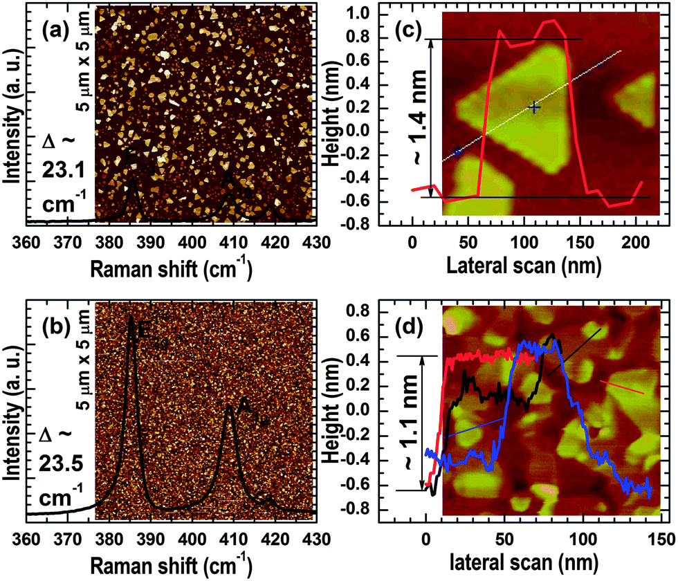 | ||
| Fig. 2 Raman scattering spectra and AFM images. (a) Raman spectrum and AFM image collected from MoS2 by MoO3 sulfurization. (b) Raman spectrum and AFM image collected from MoS2 by Mo sulfurization. (c) and (d) Are the corresponding AFM images with larger magnifications of (a) and (b); the spectra are grain height profiles. | ||
A comparison between the AFM images in Fig. 2(c) and (d) shows that the lateral island/grain size is reduced by using Mo instead MoO3 as the starting material; however, the image comparison between Fig. 2(a) and (b) reveals that the grain density is significantly improved by the Mo sulfurization. It is also found that the grain density of the resultant MoS2 layer can be increased by increasing the thickness of the starting MoO3 layer. Unfortunately, by doing so, the thickness of the resultant MoS2 is also increased, which is undesirable in the growth of 2D materials. In this regard, we focus our growth of 2D Mo1−xWxS2 ternary alloys on sulfurizing Mo1−xWx thin films.
XPS was employed to analyse the chemical compositions of the 2D Mo1−xWxS2 materials grown via Mo1−xWx sulfurization. Fig. 3(a)–(c) show the XPS spectra of S2p, Mo3d, and W4f, respectively. The peak intensities were normalized to S2p while the binding energies were aligned to C1s (285 eV). It can be seen that the core level binding energies of S2p, Mo3d, and W4f measured from the samples with x = 0 and 1 are almost identical to those of MoS2 and WS2 reported in the literature.17,24,25,35,36 It can also be seen that the peak intensities of Mo3d monotonically decrease and the peak intensities of W4f monotonically increase with the increase in the power ratios of W/(Mo + W). Chemical analyses of the 2D Mo1−xWxS2 films are carried out using the Avantage 4.12 software, which reveals that x increases from 0 to 0.25, 0.51, 0.87, and 1 as the power ratio of W/(Mo + W) increases from 0 to 0.19, 0.55, 0.85, and 1. These W contents are plotted in Fig. 3(d) as a function of power ratios of W/(Mo + W). One can see that the W content in Mo1−xWxS2 nearly linearly increases with the increase in the power ratio of W/(Mo + W). It is worth noting that the stoichiometric ratios of S to Mo1−xWx are close to 2 in the atomically thin layers, confirming the growth of Mo1−xWxS2 alloys.
 | ||
| Fig. 3 XPS spectra. (a)–(c) Are the core levels of S2p, Mo3d, and W4f. (d) Plot of W content obtained by XPS vs. power ratios of W/(Mo + W) applied for growing the individual Mo1−xWxS2 samples. | ||
It can also be clearly seen in Fig. 3(a)–(c) that the Mo3d and W4f peaks monotonically shift to lower binding energies while the S2p peak shifts to higher ones as the W content is increased in the 2D Mo1−xWxS2 alloys, although the shifts are quite small (≤0.2 eV) and are non-negligible. Chemically, such a small shift in the binding energy of the core levels can be related to a variation in the strength with which the element attracts an electron to itself; a shift of the core level to lower binding energies implies enhanced electron-attraction strength and a shift to lower binding energies implies reduced electron attraction strength. In this regard, the observed shifts in S2p, Mo3d, and W4f core levels manifest themselves as a weakening in the electron-attraction strength of S and a strengthening in the electron-attraction strength of Mo induced by the incorporation of W in Mo1−xWxS2. This phenomenon is physically expected since the electron affinity of W (0.8163 eV) is larger than that of Mo (0.7473 eV).37,38 The monotonic shifts in the core levels of S2p, Mo3d, and W4f thus suggest that the W atoms were randomly alloyed with MoS2 by substitutionally replacing Mo in the 2D crystal lattice without any phase separations.
Fig. 4 shows the optical absorbance spectra measured from the 2D Mo1−xWxS2 film samples. Two prominent absorption peaks, known as excitons A (the one at lower energy) and B (the one at higher energy),2,17 can be clearly identified in the individual spectra. These resonances have been well established to the direct excitonic transitions at the K point of the first Brillouin zone.2,39 The energy difference between excitons A and B originates from the spin-orbital splitting of the valence band, which can be experimentally derived from the individual absorbance spectra. The inset in Fig. 4 plots the exciton energies of A and B as well as their energy difference as a function of W content. It can be seen that an incorporation of 25% W in Mo1−xWxS2 shifts exciton A to a lower energy and exciton B to a higher energy; a further increase in W incorporation monotonically shifts both excitons A and B to higher energies. However, the energy difference between the A and B transitions nearly linearly increases with the increase in W content from x = 0 to x = 1, indicating that the bowing parameters of excitons A and B are close to each other. These results, as well as the initial red-shift and then blue-shift of exciton A with the increase in W content, are consistent with those observed by Chen et al. in monolayer Mo1−xWxS2 flakes obtained by mechanical exfoliation.31 It is worth to note that Mo and W atoms are randomly mixed in the lattice sites of the 2D Mo1−xWxS2 alloys. We can draw this conclusion because the exciton energy A of WS2 is significantly larger than that of MoS2 (see Fig. 4); if Mo and W formed domains with phase separations, then the convolution exciton energy A of the sample with x = 0.25 should be larger, rather than the observed smaller, than that of MoS2. In fact, the random mixing of Mo and W atoms in the 2D Mo1−xWxS2 alloys is consistent with the theoretical studies by Komsa et al.30 and the experimental work by Dumcenco et al.40
 | ||
| Fig. 4 Optical absorbance spectra. ExA and ExB indicate the excitonic resonances A and B of MoS2. The inset plots the energy and energy difference of excitons A and B vs. W content of the individual Mo1−xWxS2 samples. | ||
In terms of the absorbance in the wavelength range of 460–940 nm (see Fig. 4) the Mo1−xWxS2 films are about one-to-two monolayers in thickness, assuming that the films are uniform and continuous,2 which is consistent with the AFM observations discussed above (see Fig. 2). However, these thicknesses obtained by AFM and absorbance spectroscopy are slightly smaller than those of two-to-four monolayers estimated from the Raman spectra [see Fig. 2(a) and (b)]. Such variations can be due to (i) experimental errors in AFM measurements induced by the surface- and interface-roughness, (ii) reductions in optical absorbance induced by the boundaries/isolations between adjacent grains, and (iii) phonon shifts and thus the frequency difference between E12g and A1g induced by disordering (due to the reduced lateral grain sizes), residual crystal strain, and/or the Mo1−xWxS2/sapphire interface.41
Composition-dependent spectral evolutions of Raman scattering from the 2D Mo1−xWxS2 alloy samples are presented in Fig. 5(a), where the spectral intensities were normalized to A1g located in the range of 405–425 cm−1. It can be seen that when the W content is increased (i) the A1g mode shifts to higher energies accompanied by peak splitting, typically seen at x = 0.51, (ii) the E12g mode of MoS2 shifts to lower energies accompanied by intensity reduction, and (iii) a new mode emerges at about 355 cm−1 and shifts to higher energies towards the E12g mode of WS2, accompanied by increasing intensity. The Raman shifts of the observed phonon modes can be derived by peak-fittings using Lorentzian line shape functions. The results are plotted in Fig. 5(b) as a function of the W content, which exhibit almost linear variation behaviors from x = 0 to 1. In general, there are two sets of E12g–A1g pairs, they are far apart in terms of phonon energy at a certain composition x and degenerate to the modes of the parent binary compound at either x = 0 or x = 1. These nearly linear mode-shift behaviors and the peak intensity evolutions of E12g and A1g clearly indicate that both the in-plane mode E12g and the out-of-plane mode A1g of the 2D Mo1−xWxS2 alloy have a two-mode behavior, i.e., consist of MoS2-like and WS2-like branches. These results are also consistent with those observed in monolayer W1−xMoxS2 flakes obtained by mechanical exfoliation.31
 | ||
| Fig. 5 Raman scattering spectra. (a) Raman spectra collected from the Mo1−xWxS2 samples with different W content. (b) Raman shifts of the phonon mode derived by spectral fittings using Lorentzian line shape functions. | ||
The two-mode behavior of E12g in the 2D Mo1−xWxS2 alloys is readily understandable since it involves both the anion and cation, displacing in-plane and in opposite directions. The anion posses the lightest mass while the cations have a large difference in their masses that allow the alloy lattice to vibrate with two different E12g frequencies.34,42,43 On the contrary, the two-mode behavior of A1g is relatively complicated since only the anion is involved in this out-of-plane vibration mode and thus the frequency of A1g is not affected by the cation mass. However, as we have discussed above, the electron-attraction strength of S in Mo1−xWxS2 is reduced with the increase in W incorporated due to the larger electron affinity of W than that of Mo [see the XPS results in Fig. 3(a)–(c)]. It has also been reported that the bond length in atomically thin WS2 (0.2401 nm) is shorter than that in atomically thin MoS2 (0.2417 nm).44 As a consequence, the covalent bond length of S–Mo is varied via randomly replacing Mo by W in the 2D crystal lattice, which, together with the weak internal electrostatic coupling,33,34,42,43 allows the two A1g branches originating from the WS2- and MoS2-like sublattices.
Finally, to study the uniformity of the 2D Mo1−xWxS2 thin films, we have collected and carried out peak-fittings of the Raman spectra across the 2-inch wafer of the Mo0.49W0.51S2 sample. The mode frequencies of the two A1g branches as well as their FWHM (full-width at half-maximum) and intensity ratios are shown in Fig. 6(a), (b) and (d), respectively. The photograph shown in Fig. 6(c) was recorded using an image scanner. The fringes at the wafer edge were formed due to air trapped between the wafer surface and the scanner glass. It can be seen that the variations in the mode frequencies [Fig. 6(a)] and their line-widths [Fig. 6(b)] are smaller than 0.5 cm−1 and 0.15 cm−1, respectively. The variation in the intensity ratios of MoS2-like A1g to WS2-like A1g across the 2-inch wafer is about 5% [Fig. 6(d)]. These results, together with the smooth and uniform color of the image in Fig. 6(c), provide clear-cut evidence for the high uniformity of the atomically thin Mo1−xWxS2 ternary alloys in wafer scale.
 | ||
| Fig. 6 Phonon features of Raman scattering spectra collected across the 2-inch Mo0.49W0.51S2 sample grown on c-plane sapphire substrate. (a) Raman shifts of the WS2- and MoS2-like A1g. (b) FWHMs of the WS2- and MoS2-like A1g. (c) Photograph obtained by image scanner, the appearance of fringes at the wafer edge is due to air trapped between the wafer surface and the scanner glass. (d) Intensity ratios of MoS2-like A1g to WS2-like A1g. | ||
4. Conclusion
In conclusion, we have grown atomically thin Mo1−xWxS2 ternary compound films with x increased from 0 through 0.19, 0.51, and 0.87 to 1 by sulfurizing Mo1−xWx thin films. The Mo1−xWx thin films were deposited on 2-inch c-plane sapphire substrates at room temperature by employing a co-sputtering technique. The obtained Mo1−xWxS2 thin films consisted of crystallites of ∼50 nm in lateral scale and two-to-four monolayers in thickness. XPS studies showed that the Mo3d and W4f core levels shift (by up to 0.2 eV) to lower binding energies with the increase in W content. On the contrary, the S2p core level shifts to higher binding energies when the W content is increased. Although these core level shifts are small, they are non-negligible and can be related to the larger electron affinity of W than that of Mo. Optical absorbance spectroscopy revealed that the A exciton of Mo1−xWxS2 exhibits a red-shift at lower W contents and turns to a blue-shift with the increase in x over 25%. As a comparison, the B exciton exhibits a monotonic blue-shift from x = 0 to 1. Two-mode behavior for both the E12g and A1g phonon modes of the 2D Mo1−xWxS2 films was observed by Raman scattering. The MoS2-like A1g, WS2-like E12g, and WS2-like A1g increase while the MoS2-like E12g decreases in frequency with the increase in W content. Both the excitons shift and the two-mode behavior are consistent with those recently observed in monolayer Mo1−xWxS2 flakes obtained by mechanical exfoliation, thus exhibiting the great potential of the vapor-phase growth technique for large-scale 2D ternary transition-metal dichalcogenides.Acknowledgements
The authors would like to acknowledge S. Tripathy and S. B. Dolmanan for their help in the Raman scattering set-up. Z. Zhang is acknowledged for his help in XPS data collections.References
- Q. H. Wang, K. Kalantar-Zadeh, A. Kis, J. N. Coleman and M. S. Strano, Electronics and optoelectronics of two-dimensional transition metal dichalcogenides, Nat. Nanotechnol., 2012, 7, 699–712 CrossRef CAS PubMed.
- K. F. Mak, C. Lee, J. Hone, J. Shan and T. F. Heinz, Atomically thin MoS2: A new direct-gap semiconductor, Phys. Rev. Lett., 2010, 105, 136805 CrossRef.
- H. Wang, L. Yu, Y. Lee, Y. Shi, A. Hsu, M. L. Chin, L. Li, M. Dubey, J. Kong and T. Palacios, Integrated circuits based on bilayer MoS2 transistors, Nano Lett., 2012, 12, 4674–4680 CrossRef CAS PubMed.
- B. Radisavljevic, A. Radenovic, J. Brivio, V. Giacometti and A. Kis, Single-layer MoS2 transistors, Nat. Nanotechnol., 2011, 6, 147–150 CrossRef CAS PubMed.
- J. Yoon, W. Park, G. Bae, Y. Kim, H. S. Jang, Y. Hyun, S. K. Lim, Y. H. Kahng, W. Hong, B. H. Lee and H. C. Ko, Highly flexible and transparent multilayer MoS2 transistors with graphene electrodes, Small, 2013, 9, 3295–3300 CAS.
- J. Pu, Y. Yomogida, K. Liu, L. Li, Y. Iwasa and T. Takenobu, Highly flexible MoS2 thin-film transistors with ion gel dielectrics, Nano Lett., 2012, 12, 4013–4017 CrossRef CAS PubMed.
- H. Y. Chang, S. Yang, J. Lee, L. Tao, W. S. Hwang, D. Jena, N. Lu and D. Akinwande, High-performance, high bendable MoS2 transistors with high-k dielectrics for flexible low-power systems, ACS Nano, 2013, 7, 5446–5452 CrossRef CAS PubMed.
- A. Splendiani, L. Sun, Y. Zhang, T. Li, J. Kim, C. Chim, G. Galli and F. Wang, Emerging photoluminescence in monolayer MoS2, Nano Lett., 2010, 10, 1271–1275 CrossRef CAS PubMed.
- R. S. Sundaram, M. Engel, A. Lombardo, R. Krupke, A. C. Ferrari, Ph. Avouris and M. Steiner, Electroluminescence in single layer MoS2, Nano Lett., 2013, 13, 1416–1421 CAS.
- A. K. M. Newaz, D. Prasai, J. I. Ziegler, D. Caudel, S. Robinson, R. F. Haglund, Jr and K. I. Bolotin, Electrical control of optical properties of monolayer MoS2, Solid State Commun., 2013, 155, 49–52 CrossRef CAS PubMed.
- K. F. Mak, K. He, J. Shan and T. F. Heinz, Control of valley polarization in monolayer MoS2 by optical helicity, Nat. Nanotechnol., 2012, 7, 494–498 CrossRef CAS PubMed.
- H. Zeng, J. Dai, W. Yao, D. Xiao and X. Cui, Vally polarization in MoS2 monolayer by optical pumping, Nat. Nanotechnol., 2012, 7, 490–493 CrossRef CAS PubMed.
- S. Wu, J. S. Ross, G. Liu, G. Aivazian, A. Jones, Z. Fei, W. Zhu, D. Xiao, W. Yao, D. Cobden and X. Xu, Electrical tuning of valley magnetic moment through symmetry control in bilayer MoS2, Nat. Phys., 2013, 9, 149–153 CrossRef CAS.
- D. J. Late, B. Liu, H. S. S. R. Matte, V. P. Dravid and C. N. R. Rao, Hysteresis in single-layer MoS2 field effect transistors, ACS Nano, 2012, 6, 5635–5641 CrossRef CAS PubMed.
- K. S. Novoselov, D. Jiang, F. Schedin, T. J. Booth, V. V. Khothevich, S. V. Morozov and A. K. Geim, Two-dimensional atomic layers, Proc. Natl. Acad. Sci. U. S. A., 2005, 102, 10451–10453 CrossRef CAS PubMed.
- J. N. Coleman, M. Lotya, A. O'Neill, S. D. Bergin, P. J. King, U. Khan, K. Young, A. Gaucher, S. De, R. J. Smith, I. V. Shvets, S. K. Arora, G. Stanton, H. Kim, K. Lee, G. T. Kim, G. S. Duesberg, T. Hallam, J. J. Boland, J. J. Wang, J. F. Donegan, J. C. Grunlan, G. Moriarty, A. Shmeliov, R. J. Nicholls, J. M. Perkins, E. M. Grieveson, K. Theuwissen, D. W. McComb, P. D. Nellist and V. Nicolosi, Two-dimensional nanosheets produced by liquid exfoliation of layered materials, Science, 2011, 331, 568–571 CrossRef CAS PubMed.
- G. Eda, H. Yamaguchi, D. Voiry, T. Fujita, M. Chen and M. Chhowalla, Photoluminescence from chemically exfoliated MoS2, Nano Lett., 2011, 11, 5111–5116 CrossRef CAS PubMed.
- V. Nicolosi, M. Chhowalla, M. G. Kanatzidis, M. S. Strano and J. N. Coleman, Liquid exfoliation of layered materials, Science, 2013 DOI:10.1126/science.1226419.
- J. H. Warner, M. H. Rümmeli, A. Bachmatiuk and B. Büchner, Atomic resolution imaging and topography of boron nitride sheets produced by chemical exfoliation, ACS Nano, 2010, 4, 1299–1304 CrossRef CAS PubMed.
- A. Castellanos-Gomez, M. Barkelid, A. M. Goossens, V. E. Calado, H. S. J. van der Zant and G. A. Steele, Laser-thinning of MoS2: On demand generation of a single-layer semiconductor, Nano Lett., 2012, 12, 3187–3192 CrossRef CAS PubMed.
- Y. Huang, J. Wu, X. Xu, Y. Ho, G. Ni, Q. Zou, G. K. W. Koon, W. Zhao, A. H. C. Neto, G. Eda, C. Shen and B. Özyilmaz, An innovative way of etching MoS2: Characterization and mechanistic investigation, Nano Res., 2013, 6, 200–207 CrossRef CAS.
- Y. Lee, X. Zhang, W. Zhang, M. Chang, C. Lin, K. Chang, Y. Yu, J. T. Wang, C. Chang, L. Li and T. Lin, Synthesis of large-area MoS2 atomic layers with chemical vapor deposition, Adv. Mater., 2012, 24, 2320–2325 CrossRef CAS PubMed.
- Y. Zhan, Z. Liu, S. Najmaei, P. M. Ajayan and J. Lou, Large-area vapor-phase growth and characterization of MoS2 atomic layers on a SiO2 substrate, Small, 2012, 8, 966–971 CrossRef CAS PubMed.
- S. Najmaei, Z. Liu, W. Zhou, X. Zou, G. Shi, S. Lei, B. I. Yakobson, J. Idrobo, P. M. Ajayan and J. Lou, Vapor phase growth and grain boundary structure of molybdenum disulphide atomic layers, Nat. Mater., 2013, 12, 754–759 CrossRef CAS PubMed.
- Y. Lin, W. Zhang, J. Huang, K. Liu, Y. Lee, C. Liang, C. Chu and L. Li, Wafer-scale MoS2 thin layers prepared by MoO3 sulfurization, Nanoscale, 2012, 4, 6637–6641 RSC.
- A. L. Elías, N. Perea-López, A. Castro-Beltrán, A. Berkdemir, R. Lv, S. Feng, A. D. Long, T. Hayashi, Y. A. Kim, M. Endo, H. R. Gutiérrez, N. R. Pradhan, L. Balicas, T. E. Mallouk, F. López-Urías, H. Terrones and M. Terrones, Controlled synthesis and transfer of large-area WS2 sheets: From single layer to few layers, ACS Nano, 2013, 7, 5235–5242 CrossRef PubMed.
- W. Wu, D. De, S. Chang, Y. Wang, H. Peng, J. Bao and S. Pei, High mobility and high on/off ratio field-effect transistors based on chemical vapor deposited single-crystal MoS2 grains, Appl. Phys. Lett., 2013, 102, 142106 CrossRef.
- A. M. van der Zande, P. Y. Huang, D. A. Chenet, T. C. Berkelbach, Y. You, G. Lee, T. F. Heinz, D. R. Reichman, D. A. Muller and J. C. Hone, Grains and grain boundaries in highly crystalline monolayer molybdenum disulphide, Nat. Mater., 2013, 12, 554–561 CrossRef CAS PubMed.
- A. Berkdemir, H. R. Gutiérrez, A. R. Botello-Méndez, N. Perea-López, A. L. Elías, C. Chia, B. Wang, V. H. Crespi, F. López-Urías, J. Charlier, H. Terrones and M. Terrones, Indentification of individual and few layers of WS2 using Raman spectroscopy, Sci. Rep., 2013, 3, 1755 CrossRef PubMed.
- H. Komsa and A. V. Krasheninnikov, Two-dimensional transition metal dichalcogenide alloys: Stability and electronic properties, J. Phys. Chem. Lett., 2012, 3, 3652–3656 CrossRef CAS.
- Y. Chen, J. Xi, D. O. Dumcenco, Z. Liu, K. Suenaga, D. Wang, Z. Shuai, Y. Huang and L. Xie, Tunable band gap photoluminescence from atomically thin transition-metal dichalcogenide alloys, ACS Nano, 2013, 7, 4610–4616 CrossRef CAS PubMed.
- H. F. Liu and D. Z. Chi, Magnetron-sputter deposition of Fe3S4 thin films and their conversion into pyrite (FeS2) by thermal sulfurization for photovoltaic applications, J. Vac. Sci. Technol., A, 2012, 30, 04D102 Search PubMed.
- C. Lee, H. Yan, L. E. Brus, T. F. Heinz, J. Hone and S. Ryu, Anomalous lattice vibrations of single- and few-layer MoS2, ACS Nano, 2010, 4, 2695–2700 CrossRef CAS PubMed.
- A. Molina-Sánchez and L. Wirtz, Phonons in single-layer and few-layer MoS2 and WS2, Phys. Rev. B: Condens. Matter Mater. Phys., 2011, 84, 155413 CrossRef.
- A. P. Shpak, A. M. Korduban, L. M. Kulikov, T. V. Kryshchuk, N. B. Konig and V. O. Kandyba, XPS studies of the surface of nanocrystalline tungsten disulfide, J. Electron Spectrosc. Relat. Phenom., 2010, 181, 234–238 CrossRef CAS PubMed.
- H. G. Füchtbauer, A. K. Tuxen, P. G. Moses, H. Topsøe, F. Besenbacher and J. V. Lauritsen, Morphology and atomic-scale structure of single-layer WS2 nanoclusters, Phys. Chem. Chem. Phys., 2013, 15, 15971–15980 RSC.
- A. O. Lindahl, P. Andersson, C. Diehl, O. Forstner, P. Klason and D. Hanstorp, The electron affinity of tungsten, Eur. Phys. J. D, 2010, 60, 219–222 CrossRef CAS.
- R. C. Bilodeau, M. Scheer and H. K. Haugen, Infrared laser photodetachment of transition metal negative ions: studies on Cr−, Mo−, Cu−, and Ag−, J. Phys. B: At., Mol. Opt. Phys., 1998, 31, 3885–3891 CrossRef CAS.
- A. Ramasubramaniam, Large excitonic effects in monolayers of molybdenum and tungsten dichalcogenides, Phys. Rev. B: Condens. Matter Mater. Phys., 2012, 86, 115409 CrossRef.
- D. O. Dumcenco, H. Kobayashi, Z. Liu, Y. S. Huang and K. Suenaga, Visualization and quantification of transition metal atomic mixing in Mo1−xWxS2 single layers, Nat. Commun., 2013, 4, 1–5 CrossRef PubMed.
- H. J. Conley, B. Wang, J. I. Ziegler, Jr, R. F. Haglund, S. T. Pantelides and K. I. Bolotin, Bandgap engineering of strained monolayer and bilayer MoS2, Nano Lett., 2013, 13, 3626–3630 CrossRef CAS PubMed.
- I. F. Chang and S. S. Mitra, Application of a modified random-element-isodisplacement model to long-wavelength optical phonons of mixed crystals, Phys. Rev., 1968, 172, 924–933 CrossRef CAS.
- H. Grille, Ch. Schnittler and F. Bechstedt, Phonons in ternary group-III nitride alloys, Phys. Rev. B: Condens. Matter Mater. Phys., 2000, 61, 6091–6105 CrossRef CAS.
- H. Terrones, F. López-Urías and M. Terrones, Novel hetero-layered materials with tunable direct band gaps by sandwiching different metal disulfides and diselenides, Sci. Rep., 2013, 3, 1549 CrossRef PubMed.
| This journal is © The Royal Society of Chemistry 2014 |