DOI:
10.1039/C3NR03896C
(Paper)
Nanoscale, 2014,
6, 424-432
β-Sialon nanowires, nanobelts and hierarchical nanostructures: morphology control, growth mechanism and cathodoluminescence properties†
Received
27th July 2013
, Accepted 1st October 2013
First published on 7th October 2013
Abstract
Morphology control of one dimension (1D) nanomaterials is a pivotal issue in the field of nanoscience research to exploit their novel properties. Herein, we report the morphology controlled synthesis of 1D β-Sialon nanowires, nanobelts and hierarchical nanostructures via a thermal-chemical vapour deposition process using an appropriately selected catalyst and optimized temperature schedule. Vapour–solid (VS), a combination of vapour–liquid–solid (VLS)-based and VS-tip, and a combination of VS for one-generation nanowires with nucleation, growth and coalescence of two-generation nanobranches (NGCB) are used to explain the growth of β-Sialon nanowires, nanobelts and hierarchical nanostructures, respectively. Cathodoluminescence measurements show that the individual β-Sialon 1D nanostructures with different morphologies have different luminescent properties. All nanostructures exhibit two distinct emission peaks, the violet/blue emission centered at ∼390 nm (3.18 eV), attributable to the near band edge (NBE) emission, and the red emission centered at ∼728 nm (1.70 eV), assigned to the deep level (DL) emission. However, the DL emission is the ruling emission in the case of an individual β-Sialon nanowire, whereas the NBE emission becomes dominant in the case of an individual nanobelt as well as a hierarchical nanostructure due to the size and surface effects. The as-synthesized β-Sialon with controlled nanostructures and various morphologies can find potential applications in future nanodevices with tailorable or tunable photoelectric properties.
1. Introduction
One-dimensional (1D) nanostructured materials such as nanotubes, nanorods, nanowires and nanobelts have stimulated intense worldwide interest since the discovery of carbon nanotubes.1,2 To date, they have been successfully synthesized in different material systems, such as metal substances,3 binary oxides,4 sulfides,5 carbides,6 nitrides7 and multiple components.8 Their unique geometries and excellent properties make them useful for promising applications ranging from nanoelectronics,2b,c energy conversion and storage,2d and lasers7a to light/field emission devices.5a,6a,7b Pivotal to realizing their versatile applications is to rationally tailor the vital parameters of nanomaterials (e.g. chemical composition, structure, size and morphology).9 The past few years have witnessed significant advances in the morphology controlled synthesis of 1D nanomaterials including ZnO, Al2O3, InN and In2Ge2O7.9,10
β-Sialons are one type of solid solutions of β-Si3N4, represented by the formula Si6−zAlzOzN8−z (0 < z ≤ 4.2) where Si4+ and N3− are partially replaced by Al3+ and O2−, respectively. The substitutions only increase their crystal unit sizes instead of changing the crystal structures.11 β-Sialons exhibit excellent properties such as high strength and hardness, good corrosion and oxidation resistances, and hence, their bulk materials have attracted considerable attention for engineering applications such as use as refractories, cutting materials, high performance ceramics, oxidation and corrosion resistant materials at high temperature in aerospace.11,12 Similar to the III-N compounds, β-Sialons also can be excellent host materials because of their high dopant concentration, good mechanical/thermal properties and chemical stability, and consequently, their nanostructures could be potentially used to build smart nanodevices used in high-temperature and radiation environments.13 In recent years, considerable efforts have been made to synthesize 1D β-Sialon nanostructures, such as nanowires,14 nanotubes15 and nanobelts.13a,16 However, to our knowledge, the controlled growth of β-Sialon nanostructures with variable morphologies has not been achieved until now. According to the classical optical waveguide theory, waveguides of the nanostructures with different cross sections will display different transverse optical (TO) modes.17 Therefore, it is necessary to characterize the luminescence properties of individual β-Sialon nanostructures.
In this work, the morphology-controlled growth of β-Sialon nanostructures, including nanowires, ultra-long nanobelts and hierarchical nanostructures, have been successfully achieved by a thermal-chemical vapour deposition (CVD) reaction of Si, Al, and Al2O3 powders. Proper selections and optimization of the growth conditions (catalyst, temperature schedule) were the key factors in the morphology control. In most cases, the growth of 1D nanostructures at high temperatures could be best explained by vapour–liquid–solid (VLS) and vapour–solid (VS) mechanisms. Herein, apart from these two mechanisms for explaining the growth of β-Sialon nanowires and nanobelts, we propose a new mechanism, namely, the nucleation, growth and coalescence of nanobranches for explaining the growth of β-Sialon hierarchical nanostructures. The detailed growth mechanisms for the various β-Sialon nanostructures were discussed. Cathodoluminescence (CL) is one of the most widely used techniques to investigate optical properties of individual nanostructures because of its high spatial resolution and surface sensitivity.18 So it was used to examine optical properties of various individual β-Sialon nanostructures, which are of benefit not only for understanding the relationships among morphology, structure and luminescence properties of β-Sialon, but also for developing new generation nanodevices with tailorable or tunable photoelectric properties.
2. Experimental procedures
The syntheses of β-Sialon nanowires, nanobelts, and hierarchical nanostructures were based on the thermal CVD reaction of Si, Al, and Al2O3 powders in a conventional horizontal tube furnace (the experimental setup is shown in Fig. 1). The raw material powders were weighed according to the composition of β-Sialon (Si6−zAlzOzN8−z) with z = 2, and mixed and milled for 1 h in a ball mill. In each run of the tests, 2 g of the mixed batch was loaded in a corundum boat placed in the centre of a long horizontal corundum tube inserted in an electric furnace. Morphology control of the nanostructures was realized by properly selecting the growth conditions shown in Fig. 1 and described in detail as follows. In a typical synthesis procedure of β-Sialon nanowire (Route 1 in Fig. 1), a graphite felt without any catalyst was used to cover the corundum boat, about 1 cm away from the raw materials. The tube was purged 5 times with N2 to remove the air, and then heated from room temperature to 1450 °C at 2 °C min−1 and held for 3 h in flowing N2 (purity 99.999%). The fired samples were allowed to furnace-cool to room temperature at 3 °C min−1. For the β-Sialon nanobelts synthesis (Route 2 in Fig. 1), while keeping other experimental conditions invariant, a graphite felt coated with a 0.1 g L−1 nickel nitrate solution and dried in an oven at 100 °C was used to cover the corundum boat for the growth of products. Regarding the synthesis of hierarchical nanostructures, this was achieved by changing the firing schedules (Route 3 in Fig. 1), i.e., initially firing the samples from ambient temperature to 1450 °C at a rate of 2 °C min−1, holding for 1 h, and then raising the temperature to 1500 °C at 2 °C min−1 and holding for 2 h.
 |
| | Fig. 1 A schematic experimental setup for 1D β-Sialon nanostructures synthesis by three comparative routes. Route 1 for generating nanowires: graphite felt without catalyst heated at 1450 °C for 3 h; Route 2 for growing nanobelts: graphite felt coated with Ni(NO3)2; Route 3 for forming hierarchical nanostructures: graphite felt without catalyst heated initially at 1450 °C for 1 h and then at 1500 °C for 2 h. | |
Phases in the products were identified using X-ray diffraction (XRD) (D8 Advance, Bruker-AXS, Germany). Their morphologies and microstructures were characterized using scanning electron microscopy (SEM, JEOL JSM-7001F, Japan) and high-resolution transmission electron microscopy (HRTEM, FEI-Tecnai-G2-F20, Philips, Netherlands). The energy dispersive X-ray spectroscopies (EDS, INCA) linked with the SEM and the HRTEM, along with selected area electron diffraction (SAED), were employed to assist the phase identification. After the phase and structure examinations, cathodoluminescence (CL) spectra from individual β-Sialon nanostructures were collected with a high-resolution CL system at an accelerating voltage of 20 kV and a current of 130 μA by using an ultrahigh vacuum scanning electron microscope (UHV-SEM) equipped with a Gemini electron gun (Omicron, Germany) and a CL detector (Gatan mono 3 plus). The pressure in the specimen chamber was 10−3 Pa. All CL images and spectra were collected at room temperature under the same conditions to ensure a convincing comparison can be made.
3. Results and discussion
3.1. β-Sialon nanowire growth
After 3 h reaction at 1450 °C, a white layer of product was visually seen on the graphite cover without any catalyst. The product was identified by XRD as hexagonal structured Si4Al2O2N6 with lattice constants of a = 7.643 Å and c = 2.945 Å (Fig. 2), consistent with the JCPDS card no. 76-0599, space group P63/m (no. 176). It is worth mentioning that the nanobelts and hierarchical nanostructures introduced later in this paper were all identified by XRD as the same hexagonal β-Sialon crystal phase. As-synthesized products displayed 1D-like structures (Fig. 3a), typically several hundred micrometres in length. Magnified SEM images (Fig. 3b and c) further reveal that they actually were nanowires with circular cross sections (inset in Fig. 3b) of 80–200 nm in diameter. They were composed of 30.5% Si, 15.2% Al, 13.7% O and 40.6% N (atomic ratio) as revealed by EDS (Fig. 3d), corresponding to the stoichiometric composition of Si4Al2O2N6.
 |
| | Fig. 2 XRD pattern of the as-synthesized product with the Miller indices above the corresponding peaks, revealing that it consisted of Si4Al2O2N6 with a hexagonal structure (a = 7.643 and c = 2.945). | |
 |
| | Fig. 3 (a–c) SEM images and (d) EDS pattern of the products on the underside of the graphite cover without catalyst coated, indicating the formation of Sialon nanowires. | |
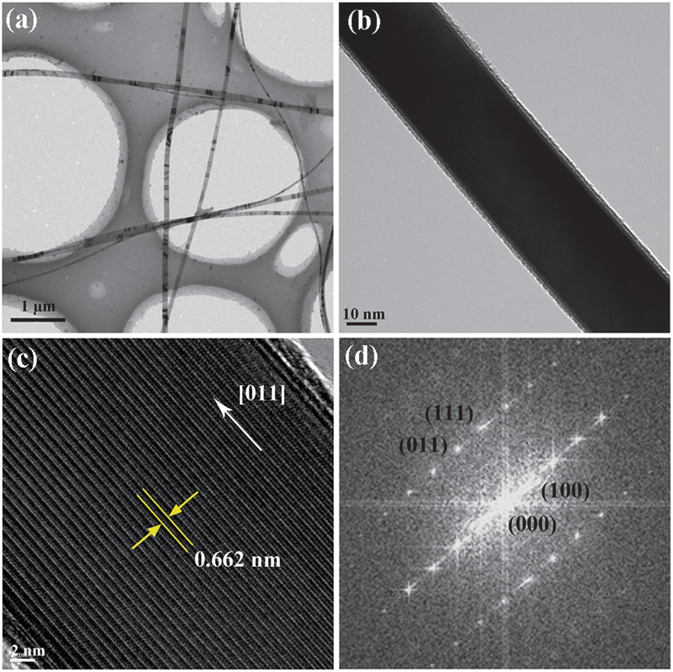
Fig. 4a and b are typical low magnification TEM images, showing the typical wire-like geometry of β-Sialon with a uniform width along its entire length. The ripple-like contrast in some nanowires is due to the residual stress, which is normally observed in TEM studies.19 An HRTEM lattice image of a typical β-Sialon nanowire (depicted in Fig. 4c) reveals that the marked interplanar d-spacing was of ca. 0.662 nm, which corresponds to the (100) lattice plane of β-Sialon. The SAED pattern by inverse fast Fourier transform (FFT) (Fig. 4d) from the nanowire reveals its single crystalline nature and the growth direction close to the [011] direction.
 |
| | Fig. 4 (a and b) TEM images, (c) HRTEM image of nanowires and (d) SAED pattern by inverse fast Fourier transform. | |
3.2. β-Sialon nanobelts growth
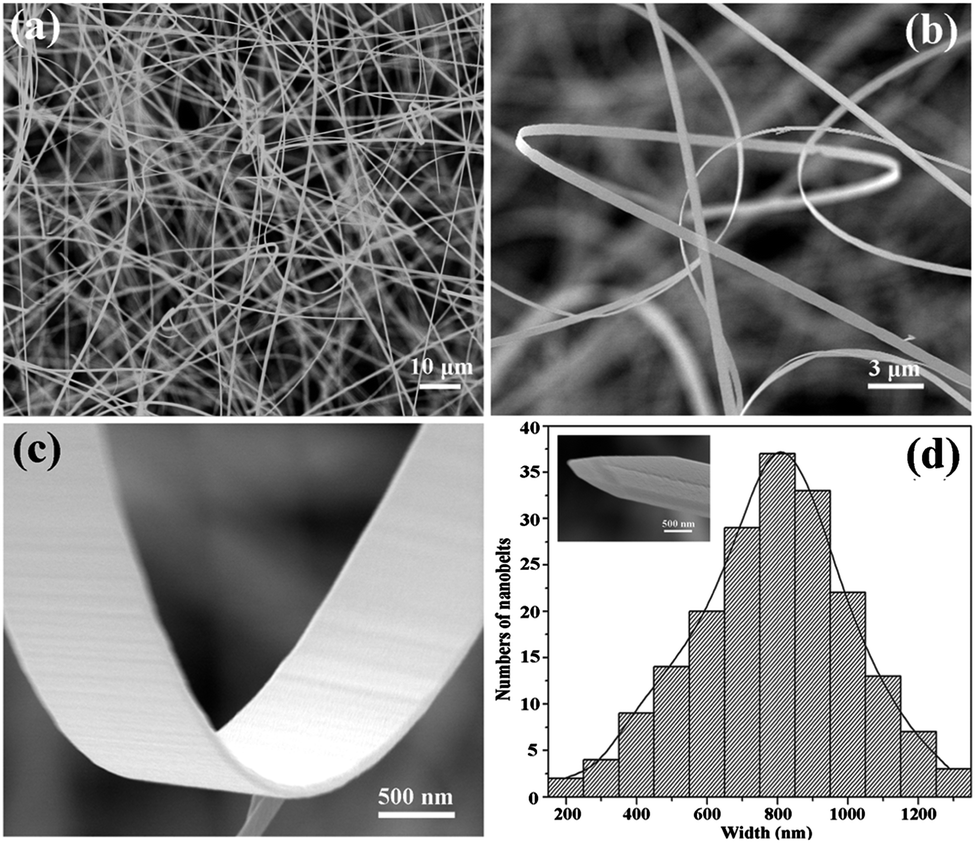
While β-Sialon nanowires were synthesized on a graphite felt without using a catalyst, nanobelts were successfully obtained on a graphite felt coated with a 0.1 g L−1 nickel nitrate solution. Several millimetres-thick white fluffy layers extending from the graphite felt surface were visually seen. A relatively low-magnification SEM image (Fig. 5a) reveals that the product exhibited 1D-like structures and most of them were a few hundred microns long. High-magnification SEM images (Fig. 5b and c) further reveal that they were nanobelts with rectangular bodies and triangular tips (inset in Fig. 5d). Statistical measurements (Fig. 5d) based on the SEM images show that the as-synthesized nanobelts had widths ranging from 200 to 1300 nm (width/thickness ratios vary from 4 to 12) and presented a unimodal distribution with a peak range of 700–900 nm.
 |
| | Fig. 5 (a) Low magnification SEM image, (b and c) high magnification SEM images of the Sialon nanobelts and (d) size distribution of as-synthesized Sialon nanobelts. Inset in (d) shows the nanobelt had a triangle tip. | |
Further details about the morphologies and crystal structures of the synthesized Sialon nanobelts can be provided by TEM and HRTEM, along with SAED. Fig. 6a and b show the typical belt-like geometry of the products, and each nanobelt had a uniform width along its length and a triangle tip at its growth front (inset in Fig. 6a). The HRTEM lattice image (Fig. 6c) reveals that the nanobelt possessed a perfect crystal structure with few defects, and the corresponding selected area electron diffraction (SAED) pattern (Fig. 6d) further verifies its hexagonal single crystal structure. The marked lattice fringe d-spacing of 0.662 nm was in agreement with (100) plane of β-Sialon. The lattice fringe, along with the SAED pattern, suggest that [201] was the growth direction of the β-Sialon nanobelt.
 |
| | Fig. 6 (a and b) TEM images of the nanobelts, (c) lattice-resolved HRTEM image and (d) SAED pattern of a nanobelt. Inset in (a) is the triangle front of nanobelt. | |
By comparing the test results of the above two sections, it is notable that the products grown on the graphite felt without catalyst were β-Sialon nanowire-like structures (Fig. 3), whereas those grown on the nickel nitrate deposited graphite felt were β-Sialon nanobelts (Fig. 5). This reveals that the nickel nitrate played a critical role in the growth process of the β-Sialon nanobelts. Fig. 7a shows the catalyst particles formed on the graphite felt which was originally coated with nickel nitrate solution and then heated at 1450 °C for 5 min. In order to further identify the effect of catalyst, some short β-Sialon nanobelts which are believed to have just started to grow from the underside of the graphite felt were characterized. As shown in Fig. 7b, β-Sialon nanobelts nucleated and grew in bunches on the graphite felt seemingly in a “weed growth” mode. EDS (Fig. 7d–i) finds that their main bodies and tips contained only Si, Al, O and N but did not contain any Ni, suggesting that the overall growth process of β-Sialon nanobelts may not have been governed by the well documented vapour–liquid–solid (VLS) tip-growth mechanism.20 Interestingly, around the roots of the short nanobelts (marked by the dotted ring in Fig. 7c), Ni was detected (Fig. 7d-ii), implying that Ni provided a site for the initial nucleation and successive growth of β-Sialon nanobelts. The involved new growth mechanisms will be discussed in detail later.
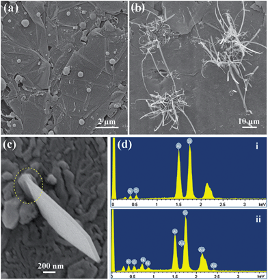 |
| | Fig. 7 SEM images of (a) the graphite felt coated with Ni(NO3)2 solution after heating at 1450 °C for 5 min, (b and c) some short β-Sialon nanobelts grown from the Ni(NO3)2-coated graphite felt in the initial stage, (d) EDS patterns of the tip (i) and root (ii) of the β-Sialon nanobelt detected in (c). | |
3.3. β-Sialon hierarchical nanostructures growth
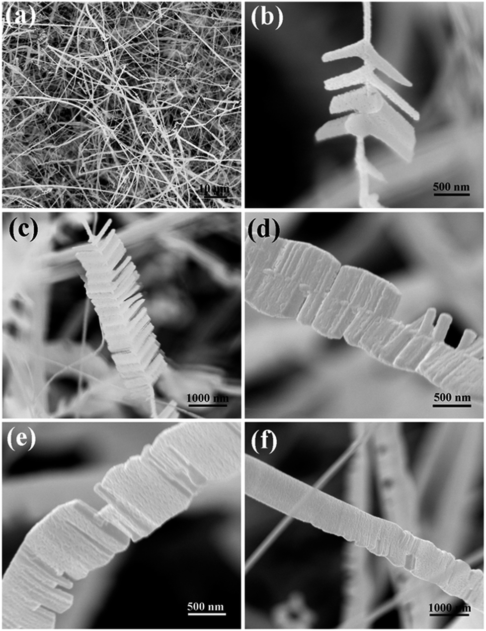
An even more interesting thing is that the two-generation hierarchical nanostructures could be produced without using a catalyst by only controlling the heating scheme, i.e., initially at 1450 °C for 1 h and then at 1500 °C for 2 h. Fig. 8a shows an SEM image of the products. Large amounts of wire-like features of several tens to hundreds microns in length were observed. A close examination of the SEM images reveals that the wire-like features were composed of two-generation hierarchical nanowires and nanobelts (ESI, Fig. S1a and b†). Upon closer inspection, several kinds of morphologies at various growth stages can be found among these β-Sialon hierarchical nanostructures (Fig. 8b–f). A dendrite-like nanostructure was composed of a first generation (1G) nanowire stem with numerous second-generation (2G) nanobranches on two opposite sides of the stem (Fig. 8b and c). The 2G nanobranches grew almost perpendicularly on the 1G nanowires and exhibited an aligned growth along the longitudinal axis. They grew along the axial direction of the stem and met with each other forming boundaries (Fig. 8d and e). The number of such boundaries was gradually reduced, suggesting the merging of different nanobranches, and finally a belt-like hierarchical nanostructure was formed (Fig. 8f). The growth manner depicted in Fig. 8 is very interesting. The structures with nanobranches have been observed previously in many material systems,21 in which the branches always grew longer along the direction perpendicular to the length direction of the stem to form a feather-like morphology. In contrast, the nanobranches in the current study grew initially perpendicularly but subsequently parallel to the length direction of the stem. The belt-like hierarchical nanostructures reported here were formed by the growth and merging of nanobranches rather than by the epitaxial growth of nuclei discussed above and reported previously.2a,7,13
 |
| | Fig. 8 (a) Low magnification SEM image of the products and (b–f) representative high magnification SEM images of the Sialon hierarchical nanostructures at various growth stages. | |
To further understand these issues, detailed analysis of the β-Sialon hierarchical nanostructures was carried out by TEM and HRTEM (Fig. 9). TEM images indicate that 1G nanowires (as shown by the yellow dotted arrows) penetrated through nanobranches or nanobelts (Fig. 9a–d). HRTEM images of Fig. 9b and c are recorded from the areas that connected the stem and the nanobranches (areas b and c marked in Fig. 9a). The darker contrast of the stem suggested that it was much thicker than the nanobranches. Upon very close observation, the lattice fringes with d-spacing of 0.276 nm corresponding to the (101) lattice planes in the bilateral branches were nearly the same as those in stems though the crystalline extent in the stems was higher than that in the branches. Fig. 9e and f are the HRTEM images of areas (e and f) marked in Fig. 9d, indicating that the nanobranches formed in the early stage subsequently joined together along the stem growth direction leaving boundaries and notches. The marked interplanar d-spacings almost matched among the conjoined branches, which were ca. 0.662 nm corresponding to the (100) lattice planes. Both these lattice fringes and inverse FFT patterns reveal that the growth direction of the stem was along [100]. And the nanobranches formed on ±(001) surfaces of the stem, initially grew along [001] and subsequently along [100], i.e., parallel to the axial direction of the stem, leading to the widening growth of the nanobranches. EDS results (ESI, Figs. S1b and c†) reveal that the nanobranch and the stem possessed a homogeneous nucleation. Based on the analysis above, the formation of β-Sialon hierarchical nanostructures could be regarded as the two-dimensional nucleation and atom stacking along certain crystallographic directions. Their formation mechanism will be discussed later.
 |
| | Fig. 9 (a) and (d) TEM of β-Sialon hierarchical nanostructures, (b) and (c) HRTEM images of areas b and c marked in (a), respectively, (e and f) HRTEM images of areas e and f marked in (d), respectively. Insets in (e and f) are the Fast Fourier transforms (FFTs) of the relevant HRTEM images. | |
3.4. Growth mechanism
In the growth mechanisms of 1D nanostructures prepared by thermal-CVD method explained previously, the involvement of vapour phase was necessary and played an important role in their formation process. In this work, although the growth conditions of three samples were distinct, the vapour phases involved should be generated from the raw materials of Si, Al and Al2O3via the same following reactions:22| | | 2Si(s) + Al2O3(s) → 2SiO(g) + Al2O(g) | (1) |
| | | 4Al(l) + Al2O3(s) → 3Al2O(g) | (2) |
However, the growth mechanisms of as-synthesized β-Sialon nanowires, nanobelts and hierarchical nanostructures should be diverse depending on different growth conditions, which could be schematically illustrated in Fig. 10 and discussed in the following sections.
 |
| | Fig. 10 Simplified growth models of β-Sialon (I) nanowires; (II) nanobelts; and (III) hierarchical nanostructures. I: (a) formation of vapours, (b) nucleation of a β-Sialon seed and (c) VS growth for the β-Sialon nanowire; II: (a) the decomposition and reduction of Ni(NO3)2 to form a Ni particle, (b) Ni–Si–Al–O–N transition liquid drop, (c) nucleation of Sialon, (d) VLS-base growth for the Sialon proto-nanobelt, (e) VS-tip growth and VLS base-growth for the Sialon nanobelt and (f) final long Sialon nanobelt; III: (a) nanobranches nucleation and growth, (b) branches widening and coalescing and (c) coalescence nearly finished, leaving boundaries and notches. | |
VS mechanism for the as-synthesized β-Sialon nanowires.
For the as-synthesized Sialon nanowires formed at 1450 °C without catalyst assistance, the formation process was governed by the so-called VS mechanism. Firstly, the raw materials were reacted or vapourized into gaseous phases (eqn (1)–(3), Fig. 10Ia), then the gaseous phases were transported and condensed on the graphite felt to nucleate the β-Sialon seeds (eqn (4), Fig. 10Ib) which grew continuously and finally formed the β-Sialon nanowires (Fig. 10Ic).| | | SiO(g) + Al2O(g) + 3Si(g) + 3N2(g) → Si4Al2O2N6(s)(seed) | (4) |
VLS-base and VS-tip mechanisms for the as-synthesized β-Sialon nanobelts.
The results and analysis in Section 3.2 reveal that the deposition of Ni(NO3)2 was crucial in the β-Sialon nanobelt growth process. Upon heating to 260 °C, Ni(NO3)2 would start to decompose and form NiO particles on the graphite felt (eqn (5)).23 With further heating, the formed NiO particles would be reduced to small Ni particles by carbon from the graphite felt surface (eqn (6), Fig. 7a and 10IIa), which would offer catalytically active sites for the subsequent nucleation and growth of the β-Sialon nanobelts.| | | 2Ni(NO3)2 → 2NiO + 4NO2 + O2 | (5) |
At the test temperature (1450 °C), the generated vapour phases from the reactions (1)–(3) could interact with nitrogen and the Ni particles, forming eutectic Ni–Si–Al–O–N liquid droplets (Fig. 10IIb). When the composition of Si–Al–O–N in droplets became supersaturated, the nucleation would start, and would then followed by the formation of proto-nanobelts of β-Sialon (eqn (7), Fig. 10IIc). To form these proto-nanobelts instead of nanowires, the initial growth along the width direction should be quicker than in the thickness direction, but the growth in the two directions would stop after some time due to the limited-size constraint of the liquid droplets.24 Thus, after the formation of the nanobelt-templates, the successive growth only along the length direction would be favored. In this case, the growth would be sustained by the continuous dissolution of Si, Al, O and N into the liquid droplets. Such a VLS base-growth mechanism instead of the VLS tip-growth mechanism is supported by the presence of nickel detected in the roots of the nanobelts rather than in their tips (Fig. 7c,d and 10IId). For the VLS base-growth mechanism to function, strong bonding between the catalyst and the substrate is required.25 In the present case, Although the interaction between Ni and the graphite felt was not fully understood, the bonding between them should be strong, considering the good wettability of liquid Ni on graphite (with a contact angle of 45°)26 and the good connection between the β-Sialon nanobelt root and the graphite felt (Fig. 7c). In addition, considering the triangular tips of the nanobelts (Fig. 5d and 7c), the VS-tip mechanism also could have contributed to the growth of the long β-Sialon nanobelts, after they had grown out from the droplets (Fig. 10IId). In this, those gaseous phases and N2 diffused directly to the tips and react to form in situ β-Sialon there (eqn (8)), which additionally contributes to the accelerated growth of the β-Sialon nanobelts along its length direction. In brief, the combined VLS-base growth and VS tip-growth mechanisms are responsible for the growth of the long single crystal Sialon nanobelts in the present work (Fig. 10IIe).
| | | [SiO](l) + [Al2O](l) + 3[Si](l) + 6[N](l) → Si4Al2O2N6(s)(base-growth) | (7) |
| | | SiO(g) + Al2O(g) + 3Si(g) + 3N2(g) → Si4Al2O2N6(s)(tip-growth) | (8) |
VS and NGCB mechanisms for the as-synthesized β-Sialon hierarchical nanostructures.
Based on the analysis in Section 3.3, the β-Sialon hierarchical nanostructures could be obtained without using any catalyst by only controlling the heating scheme. The mechanisms governing the formation process will now be discussed. Previous theory and investigations have shown empirically that the possibility of two-dimensional (2D) nucleation on a whisker/wire surface is related to the surface energy of the crystal, temperature, and supersaturated ratio of vapour, expressed by the following equation:27| |  | (9) |
where PN is the nucleation probability, B a constant, σ the surface energy of the whisker, k the Boltzmann constant, T the absolute temperature and α the supersaturation ratio defined by α = p/p0 (usually α > 1), where p is the actual vapour pressure, and p0 the equilibrium vapour pressure corresponding to temperature T. According to eqn (9), a lower surface energy implies a greater probability for the 2D nucleation. In other words, the surface areas of the low energy surfaces tend to increase in order to minimize the total surface energy. In the present work, although the exact surface energies of β-Sialon in the different crystal planes are unknown, their relative values should be similar to those of β-Si3N4 because of their same crystal structures. Generally, β-Si3N4 has a higher surface energy along the (001) than along the (100), thus, the material preferably grows along the [001] direction to minimize the total energy by minimizing the total surface area of the (001) plane.28 Therefore, the (001) theoretically is the preferred plane for 2D nucleation of the β-Sialon nanobranches. On the other hand, as indicated by eqn (9), a lower temperature and smaller supersaturation ratio facilitate the growth of wire-like structures. In contrast, a higher temperature and larger supersaturation ratio promote the 2D nucleation, leading to the formation of sheet-like structures.24 Therefore, after comparing the results in Section 3.1 with Section 3.3, we here advance an explanation for the growth of as-synthesized β-Sialon hierarchical nanostructures, i.e., the one-generation (1G) nanowires (stems) should initially generate at the lower temperature of 1450 °C for 1 h, then the two-generation (2G) nanobranches might nucleate and grow on the 1G stems at the elevated temperature of 1500 °C for 2 h.
Hence, we propose the growth of the β-Sialon hierarchical nanostructures could be separated into two stages. The first stage was a fast growth of β-Sialon 1G nanowires (stems) at 1450 °C by VS mechanism, as already stated above (Fig. 10I). The second stage was the nucleation, growth and coalescence of β-Sialon 2G nanobranches (NGCB) at a higher temperature of 1500 °C, as shown in Fig. 10III. To begin with, the 2G nanobranches would nucleate and grow via the aggregation of nitrogen and vapours generated from reaction (1)–(3) onto the (001) surface of the trunk β-Sialon nanowires (Fig. 8b,c and 10IIIa). Then those nanobranches grew parallel along the axial direction of the stem, resulting in the widening growth of the nanobranches (Fig. 8d, 9a and 10IIIb). Last, when the widened branches met each other, the geometrical coalescence between two neighbored branches would occur, leaving boundaries and notches (Figs. 8e, 9d–f and 10IIIc). These combined VS and NGCB mechanisms could be used to explain the formation of the long β-Sialon hierarchical nanostructures and verify the novelty of the technique developed in this work.
3.5. Cathodoluminescence properties
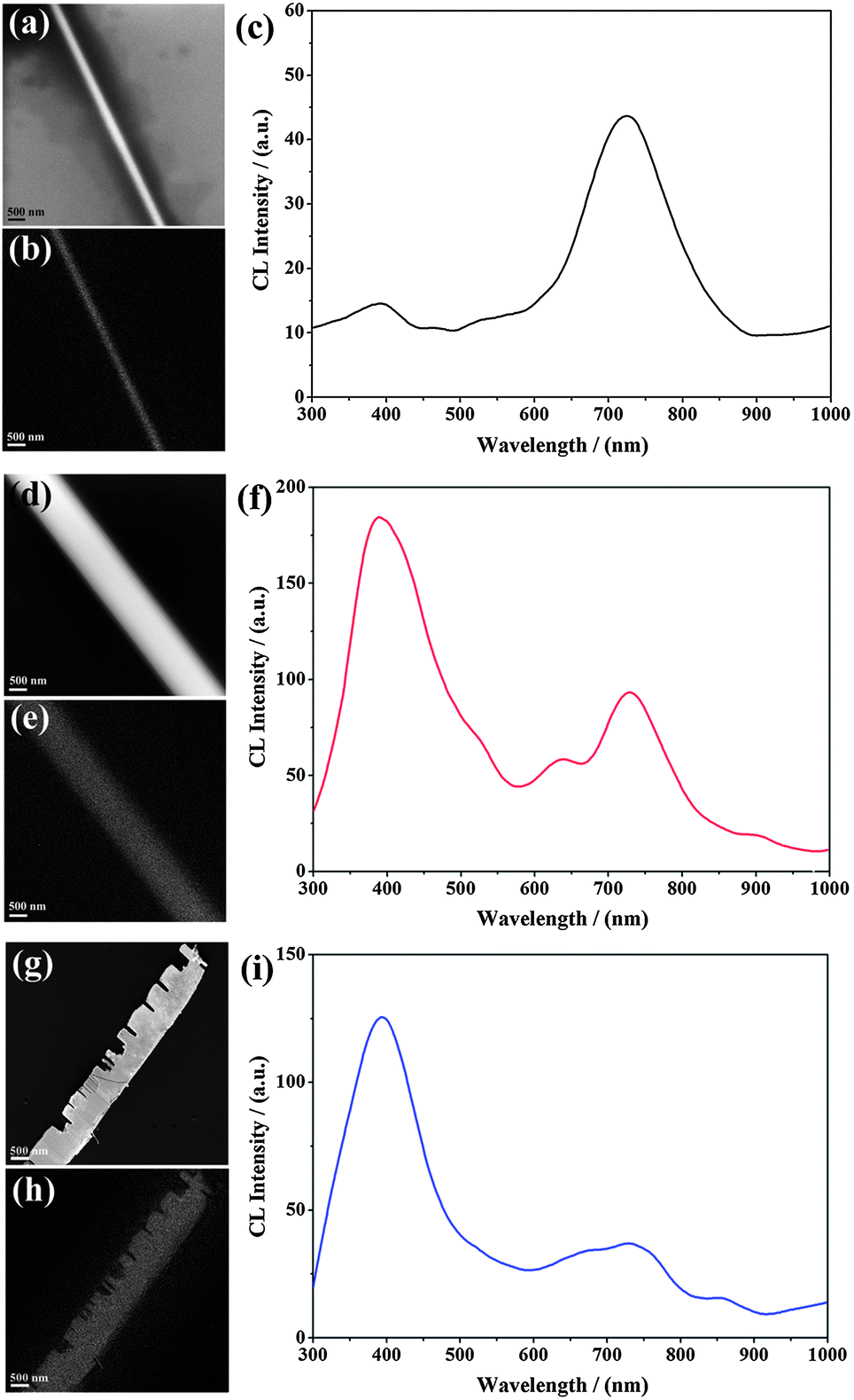
In order to investigate the optical properties of individual Sialon nanowires, nanobelts and hierarchical nanostructures, their CL spectra were recorded at room temperature. Fig. 11 presents their SEM images, CL images and spectra. All of the Sialon nanostructures demonstrated a violet/blue emission centered at ∼390 nm (3.18 eV) and a red emission centered at ∼728 nm (1.70 eV). Ching et al.29 previously made the first principles band structure calculations of β-Sialon. They pointed out that substituting Al–O for Si–N resulted in the formation of impurity-like states in the upper portion of the band-gap, which brought β-Sialons with different solute concentrations a significant decrease in the band-gap from 4.2 eV (z = 0) to 1.3 eV (z = 4). When a pair of (Al, O) atoms is substituted for a pair of (Si, N) atoms, the electron density of states becomes more complex due to the introduction of the Al–N, Al–O and Si–O bonds, which affects the lowest conduction band, and is responsible for the reduction in the band gap.28 Herein, the emission centered at ∼390 nm of β-Sialon with z ≈ 2 should be ascribed to the near band edge (NBE) emission, while the emission centered at ∼728 nm could be assigned to the deep level (DL) emission, which is related to structural defects and impurities. Such different DL/NBE luminescent mechanisms responsible for different emission ranges are not limited to Sialon in this study, but are also applicable to the cases of other nanostructures such as ZnO and CdS nanostructures, as discussed previously.18a,c,30
 |
| | Fig. 11 SEM images, CL images and room-temperature CL spectra of (a–c) individual Sialon nanowires, (d–f) nanobelts and (g–i) hierarchical nanostructures obtained with a focused electron beam at an accelerating voltage of 20 kV. All of the Sialon nanostructures exhibited violet/blue emission centered at ∼390 nm (3.18 eV) and red emission centered at ∼728 nm (1.70 eV). | |
The interesting thing is that the CL intensity of the β-Sialon nanowire was lower than that of the β-Sialon nanobelt or hierarchical nanostructure. In our CL measurements, the penetration depth of the injected electrons could reach hundreds of nanometres, or even several micrometres, under an accelerating voltage of 20 kV. Thus, the β-Sialon nanobelt and hierarchical nanostructure with bigger surfaces indicated higher intensity than the nanowires. An even more exciting thing is that the red emission band was the predominant emission in the β-Sialon nanowire with the intensity ratio of deep level to near band edge emission (IDL/INBE) of ∼2.91, whereas the relative intensity of the two emission bands varied greatly, and the violet/blue emission band came to dominate the emission with the ratio of IDL/INBE of ∼0.50 for the nanobelt, and of ∼0.30 for the hierarchical nanostructure. The different luminescent properties of the three nanostructures are understandable. A similar phenomenon has been observed before for the ZnO nanostructures by Shalish et al.30a In that case, the ratio of IDL/INBE decreased with increasing the size of the ZnO nanostructures. In this case, it should be attributed to the size and surface effects, i.e., the DL emission is the primary emission in the small size/surface nanowires, while the NBE emission becomes dominant in large size/surface nanobelts and hierarchical nanostructures.
4. Conclusion
Morphology controlled 1D β-Sialon nanowires, nanobelts and hierarchical nanostructures were synthesized by properly selecting and optimizing the growth conditions (e.g., catalyst, temperature schedule) via a thermal-chemical vapour deposition method. When a catalyst was absent, only the β-Sialon nanowires grew on the graphite felt at 1450 °C for 3 h. On the other hand, when a nickel nitrate catalyst was present, β-Sialon nanobelts instead would grow on the graphite felt under identical firing conditions. In addition, two-generation β-Sialon hierarchical nanostructures could be produced without using a catalyst by only controlling the heating scheme, i.e., initially 1450 °C for 1 h and then at a higher temperature of 1500 °C for 2 h. The β-Sialon nanowires, nanobelts, and hierarchical nanostructures grew via VS, a combination of VLS-based and VS-tip, and a combined mechanism of VS for 1G nanowires along with subsequent nucleation, growth and coalescence of 2G nanobranches (NGCB) mechanisms, respectively. The cathodoluminescence technique was used to characterize the luminescence properties of an individual β-Sialon nanowire, nanobelt and hierarchical nanostructure. All nanostructures showed two distinct emission peaks, i.e., the violet/blue emission centered at ∼390 nm (3.18 eV) and the red emission centered at ∼728 nm (1.70 eV). The former could be ascribed to the near band edge (NBE) emission, and the latter could be assigned to the deep level (DL) emission. The DL emission was the primary emission in the individual β-Sialon nanowire, while the NBE emission became dominant in individual nanobelt and hierarchical nanostructures as a result of the size and surface effects. The as-synthesized controlled β-Sialon nanostructures could find potential applications in future optoelectronic nanodevices because of their interesting optical properties.
Acknowledgements
This work was financially supported by National Natural Science Foundation of China (Grant no. 51032007), Y. G. Liu also thanks the Program for New Century Excellent Talents in University (Grant no. NCET-12-0951) and New Star Technology Plan of Beijing (Grant no. 2007A080).
Notes and references
- S. Iijima, Nature, 1991, 345, 56 CrossRef.
-
(a) Z. W. Pan, Z. R. Dai and Z. L. Wang, Science, 2001, 291, 1947 CrossRef CAS PubMed;
(b) Y. Huang, X. F. Duan, Y. Cui, L. J. Lauhon, K.-H. Kim and C. M. Lieber, Science, 2001, 294, 1313 CrossRef CAS PubMed;
(c) J. Y. Tang, Z. Y. Huo, S. Brittman, H. W. Gao and P. D. Yang, Nat. Nanotechnol., 2011, 6, 568 CrossRef CAS PubMed;
(d) B. K. Guo, X. P. Fang, B. Li, Y. F. Shi, C. Y. Ouyang, Y.-S. Hu, Z. X. Wang, G. D. Stucky and L. Q. Chen, Chem. Mater., 2012, 24, 457 CrossRef CAS;
(e) Y. Shen, J. H. Zhou, T. R. Liu, Y. T. Tao, R. B. Jiang, M. X. Liu, G. H. Xiao, J. H. Zhu, Z.-K. Zhou, X. H. Wang, C. J. Jin and J. F. Wang, Nat. Commun., 2013, 4, 2381 Search PubMed.
-
(a) H. J. Zhu, H. J. Chen, J. F. Wang and Q. Li, Nanoscale, 2013, 5, 3742 RSC;
(b) T.-Y. Kim, W.-J. Kim, S.-H. Hong, J.-E. Kim and K.-S. Suh, Angew. Chem., Int. Ed., 2009, 48, 3806 CrossRef CAS PubMed;
(c) E. B. Guidez and C. M. Aikens, Nanoscale, 2012, 4, 4190 RSC.
-
(a) L. C. Yang, L. L. Liu, Y. S. Zhu, X. J. Wang and Y. P. Wu, J. Mater. Chem., 2012, 22, 13148 RSC;
(b) A. C. Santulli, M. Feygenson, F. E. Camino, M. C. Aronson and S. S. Wong, Chem. Mater., 2011, 23, 1000 CrossRef CAS;
(c) D. Chen, Z. Liu, B. Liang, X. F. Wang and G. Z. Shen, Nanoscale, 2012, 4, 3001 RSC.
-
(a) T. Y. Zhai, X. S. Fang, Y. Bando, B. Dierre, B. D. Liu, H. B. Zeng, X. J. Xu, Y. Huang, X. L. Yuan, T. Sekiguchi and D. Golberg, Adv. Funct. Mater., 2009, 19, 2423 CrossRef CAS;
(b) A. Datta, G. Sinha, S. K. Panda and A. Patra, Cryst. Growth Des., 2009, 9, 427 CrossRef CAS;
(c) X. L. Xu, J. X. Wang, G. Y. Jing, Z. X. Shen, B. S. Zou, H. M. Fan and M. Olivo, Nanoscale, 2012, 4, 5665 RSC.
-
(a) Y. Sun, H. Cui, L. Gong, J. Chen, P. K. Shen and C. X. Wang, Nanoscale, 2011, 3, 2978 RSC;
(b) W. Xie, G. Möbus and S. W. Zhang, J. Mater. Chem., 2011, 21, 18325 RSC;
(c) L. Q. Xu, S. L. Li, Y. X. Zhang and Y. J. Zhai, Nanoscale, 2012, 4, 4900 RSC.
-
(a) M.-S. Hu, G.-M. Hsu, K.-H. Chen, C.-J. Yu, H.-C. Hsu, L.-C. Chen, J.-S. Hwang, L.-S. Hong and Y.-F. Chen, Appl. Phys. Lett., 2007, 90, 123109 CrossRef;
(b) M.-S. Hu, W.-M. Wang, T. T. Chen, L.-S. Hong, C.-W. Chen, C.-C. Chen, Y.-F. Chen, K.-H. Chen and L.-C. Chen, Adv. Funct. Mater., 2006, 16, 537 CrossRef CAS;
(c) J. T. Huang, S. W. Zhang, Z. H. Huang, Y. Wen, M. H. Fang and Y. G. Liu, CrystEngComm, 2012, 14, 7301 RSC.
-
(a) Y. Cui, G. Wang and D. C. Pan, J. Mater. Chem., 2012, 22, 12471 RSC;
(b) X. K. Zhang, S. L. Tang, J. Y. Yu, L. Zhai, Y. G. Shi and Y. W. Du, Cryst. Growth Des., 2009, 9, 2971 CrossRef CAS;
(c) L. Q. Mai, F. Yang, Y.-L. Zhao, X. Xu, L. Xu and Y.-Z. Luo, Nat. Commun., 2011, 2, 381 CrossRef PubMed;
(d) Y. Hou, X.-Y. Li, Q.-D. Zhao, X. Quan and G.-H. Chen, Adv. Funct. Mater., 2010, 20, 2165 CrossRef CAS.
- C. Y. Yan, N. D. Singh and P. S. Lee, Cryst. Growth Des., 2009, 9, 3697 CAS.
-
(a) L. P. Xu, Y.-L. Hu, C. Pelligra, C.-H. Chen, L. Jin, H. Huang, S. Sithambaram, M. Aindow, R. Joesten and S. L. Suib, Chem. Mater., 2009, 21, 2875 CrossRef CAS;
(b) K. D. Sardar, F. L. Deepak, A. G. Raj, M. M. Seikh and C. N. R. Rao, Small, 2005, 1, 91 CrossRef CAS PubMed;
(c) D. Wu, J. Liu, X. N. Zhao, A. D. Li, Y. F. Chen and N. B. Ming, Chem. Mater., 2006, 18, 547 CrossRef CAS;
(d) Y. Zhang, R. Y. Li, X. R. Zhou, M. Cai and X. L. Sun, Cryst. Growth Des., 2009, 9, 4230 CrossRef CAS.
- V. A. Izhevskiy, L. A. Genova, J. C. Bressiani and F. Aldinger, J. Eur. Ceram. Soc., 2000, 20, 2275 CrossRef CAS.
-
(a) F. L. Riley, J. Am. Ceram. Soc., 2000, 83, 245 CrossRef CAS;
(b) Z. H. Huang, J. Z. Yang, Y. G. Liu, M. H. Fang, J. T. Huang, H. R. Sun and S. F. Huang, J. Am. Ceram. Soc., 2012, 95, 859 CAS;
(c) J. Z. Yang, Z. H. Huang, M. H. Fang, Y. G. Liu, J. T. Huang and J. H. Hu, Scr. Mater., 2009, 61, 632 CrossRef CAS PubMed.
-
(a) C. L. Qin, G. W. Wen, X. Y. Wang, L. Song and X. X. Huang, J. Mater. Chem., 2011, 21, 5985 RSC;
(b) T.-C. Liu, B.-M. Cheng, S.-F. Hu and R.-S. Liu, Chem. Mater., 2011, 23, 3698 CrossRef CAS.
-
(a) D. H. L. Ng, T. L. Y. Cheung, F. L. Kwong, Y.-F. Lib and R. Yang, Mater. Lett., 2008, 62, 1349 CrossRef CAS PubMed;
(b) X. M. Hou, Z. Y. Yu, Z. Y. Chen, B. J. Zhao and K.-C. Chou, Dalton Trans., 2012, 41, 7127 RSC.
- G. H. Liu, K. X. Chen and J. T. Li, CrystEngComm, 2012, 14, 5585 RSC.
- J. T. Huang, Y. G. Liu, Z. H. Huang, M. H. Fang, S. W. Zhang, W. Xie, J. Z. Yang, S. F. Huang and Y. G. Xu, Cryst. Growth Des., 2013, 13, 10 CAS.
-
K. Okamoto, Fundamentals of Optical Waveguides, Academic, San Diego, CA, 2000 Search PubMed.
-
(a) T. Y. Zhai, X. S. Fang, Y. Bando, B. Dierre, B. D. Liu, H. B. Zeng, X. J. Xu, Y. Huang, X. L. Yuan, T. Sekiguchi and D. Golberg, Adv. Funct. Mater., 2009, 19, 2423 CrossRef CAS;
(b) J. Q. Hu, Y. Bando, T. Sekiguchi, F. F. Xu and J. H. Zhan, Appl. Phys. Lett., 2004, 84, 804 CrossRef CAS;
(c) U. K. Gautam, L. S. Panchakarla, B. Dierre, X. S. Fang, Y. Bando, T. Sekiguchi, A. Govindaraj, D. Golberg and C. N. R. Rao, Adv. Funct. Mater., 2009, 19, 131 CrossRef CAS.
-
(a) F. M. Gao, W. Y. Yang, H. T. Wang, Y. Fan, Z. P. Xie and L. N. An, Cryst. Growth Des., 2008, 8, 1461 CrossRef CAS;
(b) D. Banerjee, J. Y. Lao, D. Z. Wang, J. Y. Huang, Z. F. Ren, D. Steeves, B. Kimball and M. Sennett, Appl. Phys. Lett., 2003, 83, 2061 CrossRef CAS.
-
(a) R. S. Wagner and W. C. Ellis, Appl. Phys. Lett., 1964, 4, 89 CrossRef CAS;
(b) S. F. Huang, Z. H. Huang, M. H. Fang, Y. G. Liu, J. T. Huang and J. Z. Yang, Cryst. Growth Des., 2010, 10, 2439 CrossRef CAS.
-
(a) Z. L. Wang, X. Y. Kong and J. M. Zuo, Phys. Rev. Lett., 2003, 91, 185502 CrossRef CAS;
(b) D. B. Kuang, A. W. Xu, Y. P. Fang, H. Q. Liu, C. Frommen and D. Fenske, Adv. Mater., 2003, 15, 1747 CrossRef CAS;
(c) X. M. Wang and Y. H. Ni, RSC Adv., 2012, 2, 2340 RSC.
-
(a) M. Ksiazek, N. Sobczak, B. Mikulowski, W. Radziwill and I. Surowiak, Mater. Sci. Eng., A, 2002, 324, 162 CrossRef;
(b) X. S. Fang, C. H. Ye, L. D. Zhang and T. Xie, Adv. Mater., 2005, 17, 1661 CrossRef CAS;
(c) P. L. Dong, X. D. Wang, M. Zhang, M. Guo and S. Seetharaman, J. Nanomater., 2008, 2008, 282187 CrossRef PubMed.
- T. Y. Kim, S. H. Lee, Y. H. Mo, K. S. Nahm, J. Y. Kim, E. K. Sun and M. Kim, Korean J. Chem. Eng., 2004, 21, 733 CrossRef CAS.
-
(a) B. S. Xu, D. Yang, F. Wang, J. Liang and S. F. Ma, Appl. Phys. Lett., 2006, 89, 074106 CrossRef;
(b) W. Lu, P. Xie and C. M. Lieber, IEEE Trans. Electron Devices, 2008, 55, 2859 CrossRef CAS.
- M. Kumar and Y. Ando, J. Nanosci. Nanotechnol., 2010, 10, 3739 CrossRef CAS PubMed.
- M. Bozack, L. Swanson and A. Bell, J. Mater. Sci., 1987, 22, 2421 CrossRef CAS.
-
(a) Z. R. Dai, Z. W. Pan and Z. L. Wang, Adv. Funct. Mater., 2003, 13, 9 CrossRef CAS;
(b) Y. Zhang, R. Y. Li, X. R. Zhou, M. Cai and X. L. Sun, Cryst. Growth Des., 2009, 9, 4230 CrossRef CAS.
- J. C. Idrobo, H. Iddir, S. Öğüt, A. Ziegler, N. D. Browning and R. O. Ritchie, Appl. Phys. B, 2005, 72, 241301 Search PubMed.
- W.-Y. Ching, M.-Z. Huang and S.-D. Mo, J. Am. Ceram. Soc., 2000, 83, 780 CrossRef CAS.
-
(a) I. Shalish, H. Temkin and V. Narayamuri, Phys. Rev. B: Condens. Matter Mater. Phys., 2004, 69, 245401 CrossRef;
(b) M. Zhang, T. Y. Zhai, X. Wang, Q. Liao, Y. Ma and J. N. Yao, J. Solid State Chem., 2009, 182, 3188 CrossRef CAS PubMed.
Footnote |
| † Electronic supplementary information (ESI) available. See DOI: 10.1039/c3nr03896c |
|
| This journal is © The Royal Society of Chemistry 2014 |
Click here to see how this site uses Cookies. View our privacy policy here.