Low-frequency noise in multilayer MoS2 field-effect transistors: the effect of high-k passivation†
Junhong
Na
a,
Min-Kyu
Joo
ab,
Minju
Shin
ab,
Junghwan
Huh
c,
Jae-Sung
Kim
a,
Mingxing
Piao
a,
Jun-Eon
Jin
a,
Ho-Kyun
Jang
a,
Hyung Jong
Choi
d,
Joon Hyung
Shim
d and
Gyu-Tae
Kim
*a
aSchool of Electrical Engineering, Korea University, Seoul 136-713, South Korea. E-mail: gtkim@korea.ac.kr
bIMEP-LAHC, Grenoble INP-MINATEC, 3 Parvis Louis Neel, 38016 Grenoble, France
cDepartment of Electronics and Telecommunications, Norwegian University of Science and Technology, NO-7491 Trondheim, Norway
dSchool of Mechanical Engineering, Korea University, Seoul 136-713, South Korea
First published on 9th October 2013
Abstract
Diagnosing of the interface quality and the interactions between insulators and semiconductors is significant to achieve the high performance of nanodevices. Herein, low-frequency noise (LFN) in mechanically exfoliated multilayer molybdenum disulfide (MoS2) (∼11.3 nm-thick) field-effect transistors with back-gate control was characterized with and without an Al2O3 high-k passivation layer. The carrier number fluctuation (CNF) model associated with trapping/detrapping the charge carriers at the interface nicely described the noise behavior in the strong accumulation regime both with and without the Al2O3 passivation layer. The interface trap density at the MoS2–SiO2 interface was extracted from the LFN analysis, and estimated to be Nit ∼ 1010 eV−1 cm−2 without and with the passivation layer. This suggested that the accumulation channel induced by the back-gate was not significantly influenced by the passivation layer. The Hooge mobility fluctuation (HMF) model implying the bulk conduction was found to describe the drain current fluctuations in the subthreshold regime, which is rarely observed in other nanodevices, attributed to those extremely thin channel sizes. In the case of the thick-MoS2 (∼40 nm-thick) without the passivation, the HMF model was clearly observed all over the operation regime, ensuring the existence of the bulk conduction in multilayer MoS2. With the Al2O3 passivation layer, the change in the noise behavior was explained from the point of formation of the additional top channel in the MoS2 because of the fixed charges in the Al2O3. The interface trap density from the additional CNF model was Nit = 1.8 × 10¹² eV−1 cm−2 at the MoS2–Al2O3 interface.
Introduction
Two-dimensional (2-D) nanostructures have attracted considerable interest because of their unique properties and the easiness in fabricating the complex structures compared with three- or one-dimensional nanostructures. Among those 2-D nanostructures, graphene has drawn particular interest in recent years owing to extremely large charge carrier mobility.1 However, because of the absence of a band gap, device operation suitable for logic applications is not straightforward.2–4 Layered transition-metal dichalcogenides (TMDs) such as MoS2 have finite band gaps, and so are more appropriate for logic devices.5An electron mobility of 217 cm2 V−1 s−1 has been reported in monolayer MoS2 passivated with a high-k dielectric.6 This is a substantial improvement over the value of 3 cm2 V−1 s−1 that was reported previously.7 The large mobility of monolayer MoS2 may be an overestimate due to the wrong choice of the gate capacitance used in the dual-gate measurement system.8,9 Significant mobility improvement due to the effect of the high-k dielectrics on the MoS2 may not be as large as the initial report suggested; however, further works are required to explain the effects of the high-k dielectric on the charge carrier mobility, as well as the device characteristics of MoS2 transistors.9
Multilayer MoS2 has a comparable band gap (Eg = 1.2 eV) to that of silicon (where Eg = 1.1 eV), and a lower band gap than monolayer MoS2 (where Eg = 1.8 eV). There is therefore greater potential for multilayer MoS2 applications in wide spectral response photodetectors compared with monolayer MoS2.10 In addition, it has a relatively high electron mobility compared with either amorphous Si, low-temperature polycrystalline Si, or amorphous metal oxide semiconductors in view of thin-film transistors.10,11 The film thickness can be controlled, and very thin films, including monolayers, can be obtained from the top-down processes,12–14 which are more flexible for customizing the nanodevices.
High-k materials and semiconductors are inseparable in the nanodevice applications, particularly field-effect transistors (FETs). The high-k materials must be used for the gate dielectrics to achieve the ultimate field effect and the lower gate leakage current. Due to the fixed charges and the interface states from the high-k dielectrics, it is difficult to use the high-k for the gate insulators in the FETs. It is important not only to reduce those flaws, but also to diagnose them exactly. However, there are few works for diagnosing the interactions between the high-k and the MoS2.11,15 Therefore, in order to apply the multilayer MoS2 to the nanodevices, the effects of a high-k dielectric to the MoS2 should be understood.
The low-frequency noise (LFN) characteristics of FETs have been used to provide information relating to the interface quality between the Si channel and the gate dielectric in Si metal–oxide–semiconductor field-effect transistors (MOSFETs).16–19 As the channel length of MOSFETs continues to be reduced by the scaling of device dimensions, fluctuations in the drain current become increasingly significant, and so the importance of LFN analysis has also grown. However, very little LFN analysis of MoS2 FETs has been carried out to date.
In this article, passivation of MoS2 using high-k dielectrics such as Al2O3 and the effects on the electrical properties of multilayer MoS2 were characterized using LFN measurements.
Experimental
Bulk MoS2 crystals (SPI Supplies, USA) were mechanically exfoliated directly onto a p++ Si substrate, which was thermally grown using a 300 nm-thick SiO2 layer. Fig. 1(a) (left image) shows the as-exfoliated multilayer MoS2 on the 300 nm-thick SiO2 substrate. We can estimate the thickness of MoS2 from the optical image.20,21 The channel length (0.28 μm) and width (2.3 μm) were defined using electron beam lithography. A 10 nm-thick Ti adhesion layer followed by a 100 nm-thick Au layer was deposited using electron beam evaporation, and electric contacts were defined using a lift-off process with acetone. Fig. 1(a) (right image) shows an optical image after metallization. In Fig. 1(b), atomic force microscopy (AFM) measurements confirmed that the thickness of the multilayer MoS2 was 11.3 nm. MoS2 is a multilayered structure with an interlayer distance of ∼0.65 nm, which is consistent with the images shown in Fig. 1(c). We can therefore determine the number of layers in the structure: an 11.3 nm-thick MoS2 film contains approximately 17 layers. A schematic of the multilayer MoS2 FET is shown in Fig. 1(d) before depositing the Al2O3 passivation layer. | ||
| Fig. 1 (a) Optical images before and after the formation of source/drain metal contacts on the multilayer MoS2. The scale bar is 5 μm long. (b) AFM images of the multilayer MoS2 with the source/drain metal contacts. The inset shows that the thickness of MoS2 layer was approximately 11.3 nm. The scale bar is 2 μm long. (c) Schematic image of multilayer MoS2. The gap between monolayers is 0.65 nm. (d) Schematic image of a back-gated multilayer MoS2 FET. The source/drain contacts are Ti/Au. The back-gate is p++ Si and the gate dielectric is SiO2. | ||
The electrical properties of the FET were characterized using a Keithley 4200 semiconductor analyzer. LFN measurements were carried out using our custom LFN characterization system,22 which was configured using a data acquisition (DAQ) module. All direct current (DC) and alternating current (AC) electrical measurements were carried out in ambient air at room temperature.
A 30 nm-thick Al2O3 passivation layer was deposited on the MoS2 at 220 °C using atomic layer deposition (ALD) (Atomic Classic, CN-1 Corporation). The duration of the growth was 10 hours (300 cycles with a growth rate of 1 Å per cycle). Trimethylaluminum (TMA) (UP Chemical Co., Ltd.) and deionized (DI) water were used as precursors. Ultra-pure N2 (99.999%) was used as a carrier and purging gas. The sequence of the ALD cycle was H2O (1 s)/N2 (60 s)/TMA (1 s)/N2 (60 s). The initial pressure of the growth chamber was ∼5 × 10⁻² Torr, and it was maintained at ∼1 Torr during the deposition.
In order to ensure that thermal annealing during the ALD process did not affect the comparison between devices with and without an Al2O3 layer, a thermal annealing process with the same conditions as the ALD growth process (i.e. 220 °C, 10 hours, ∼7 × 10⁻² Torr, but with no precursors) was applied to those devices without an Al2O3 passivation layer (see the ESI for further details†). From Fig. S1,† the as-fabricated MoS2 transistor showed Schottky-like behavior in its output characteristics; however, following the thermal annealing process, ohmic-like behavior was observed. Even these relatively low-temperature thermal anneals appear to be sufficient to achieve ohmic-like behavior to MoS2 devices.
Typically, a significant increase in drain current, which was observed here following the thermal anneal, is attributed to a decrease in the contact resistance. There may be a number of reasons for this. First, remnant polymer residues, which may come from the scotch tape or the electron beam resist between the channel and the contact, may be removed during the thermal annealing process to improve the effective junction area.23 These residues can also act like an interfacial layer between the MoS2 and the metal layer and be removed by the thermal annealing.24 Another possible reason for the increase in the current is that gas molecules such as oxygen and water can be desorbed from the MoS2 surface during the annealing process. Typically, oxygen and water adsorbed onto the surface can capture electrons from the MoS2 and decrease the carrier concentration.25–28 If those molecules are desorbed from the surface, especially near the contact, it can result in a decrease of the depletion layer width in the MoS2–metal Schottky junction, followed by a decrease of the contact resistance. In order to do the precise static and LFN analysis by obtaining the linear I–V shape, therefore, the thermal annealing process should be required.
Results and discussion
Fig. 2(a) shows the typical transfer characteristics of the multilayer MoS2 transistors with and without the Al2O3 passivation. We can confirm that the MoS2 FET operates as an n-channel device. Important electrical parameters such as the field-effect mobility, μFE, the threshold voltage, Vth, and the on/off ratio are shown in Fig. 2(b) with and without the Al2O3 passivation layer. Interestingly, the on/off ratio decreased from ∼ 105 to ∼ 103 when the Al2O3 passivation layer was included, resulting from an increase in the off-current from ∼10−13 A to ∼10−10 A. In Fig. S2,† all other MoS2 transistors that we measured showed the same results, which is the off-current increase after the Al2O3 passivation. This can be explained by considering that an additional channel is induced by the Al2O3 passivation (as discussed later in the paper). If an additional channel is induced near the top of the multilayer MoS2 in parallel with the MoS2 channel, it will be difficult to deplete the additional channel by controlling the back-gate voltage because of the geometry of the gate (i.e. there is poor gate-coupling). This off-current increase due to the Al2O3 deposition is not good news for electronic device applications, but we believe that these phenomena can be reduced and removed by staking the top-gate metal on the Al2O3 high-k dielectric.29 Choosing the work function of the gate metal can naturally deplete the electrons in the channel due to the work function difference.30 Also, by controlling the top-gate bias, the electrons in the additional top channel of MoS2 can be easily modulated due to the enhancement of the gate-coupling. | ||
| Fig. 2 Changes in the DC electrical characteristics of the multilayer MoS2 FETs with and without the Al2O3 passivation. (a) Transfer characteristics without (black line) and with (red line) the Al2O3 passivation. The inset shows a logarithmic plot of the transfer characteristics. (b) On and off-current with and without the Al2O3 passivation layer, as well as the on/off ratios. The table in the inset shows the threshold voltages and μFE. | ||
The threshold voltage shifted from 11.1 V to −20.5 V by including the Al2O3 passivation. Although most of the gas molecules on the MoS2 surface – such as oxygen and water – were removed during the thermal annealing process, whatever molecules remain may be adsorbed on the MoS2 surface and can be removed during the ALD process. In addition, the overall effect of doping due to the Al2O3 layer may explain why Vth shifted. A slight increase in μFE from 8.4 to 9.9 cm2 V−1 s−1 was observed with the Al2O3 passivation layer; μFE was 17.9% larger with the high-k dielectric. These charge carrier mobilities were extracted without considering the fringing fields and the dielectric constant of the Al2O3. When these factors are taken into consideration, the capacitance was 19.2% larger for the device with the Al2O3 passivation layer (see the ESI for details of the numerical calculation of the gate capacitance†). This variation between the gate capacitance values can be compensated between the μFE values for devices without and with the Al2O3 passivation. The effects of the high-k dielectric and the thermal annealing should be separated, especially when extracting μFE. The field-effect mobility includes the effects of the contact resistance between the metal contact layer and the semiconductor channel. The suppression of Coulomb scattering in the high-k environment is one possible mechanism for an increase of μFE of MoS2,6,9,15,31 however, it is important to consider that the decrease of the contact resistance following the ALD process may occur.8,9 We have already established that the thermal annealing effects of the ALD result in a reduction in the contact resistance. An anomalous effect of the high-k dielectric on μFE was not observed in our devices. High mobility of MoS2 FETs, however, is absolutely necessary to the device applications. Using a low work function metal such as scandium for the contacts could raise the mobility value,32 and decreasing of the substrate interactions might be a way of getting the higher mobility.33 The selection of the proper number of layers might be another way to improve the mobility value.34
Fig. 3(a) and (b) show the normalized drain current spectral density (SI/Ids2) as a function of frequency (f) at different gate voltages with and without the Al2O3 passivation, respectively. In both cases, a 1/f dependence of the noise was observed. The normalized drain current spectral densities decreased as the gate voltages increased, which can be explained by considering that the noise sources were almost constant; however, as Vgs increased, the drain current also increased, resulting in a larger signal-to-noise ratio. It appears that these multilayer MoS2 transistors follow the conventional 1/f noise characteristics that have been reported for numerous nanoscale devices, including graphene,35–37 carbon nanotubes,38,39 ZnO nanowires,40,41 SnO2 nanowires,42–44 Bi2Se3 thin films.45
 | ||
| Fig. 3 LFN characteristics of the multilayer MoS2 FETs. The normalized drain current spectral density as a function of the frequency at various gate voltages is shown (a) without and (b) with the Al2O3 passivation layer. The dashed lines in the curves show the 1/f dependence. (c) The mean normalized drain current spectral density as a function of the drain current for frequencies of 10, 12, 14, 16, 18, and 20 Hz, both without (black) and with (red) the Al2O3 passivation layer. | ||
In order to directly compare the noise characteristics at a given same drain current, we plot the normalized drain current spectral density, SI/Ids2, as a function of the drain current, Ids. These data are shown in Fig. 3(c) both with and without the Al2O3 passivation. At relatively large currents, in the strong accumulation regime, the noise levels were very similar. However, at relatively low current levels, i.e. in the subthreshold regime, the noise level was higher with the Al2O3 passivation layer. It follows that the Al2O3 layer resulted in an additional noise source that could be observed at the low currents.
Two models exist to describe the LFN in conventional Si MOSFETs.16 The Hooge mobility fluctuation (HMF) model describes fluctuations of the carrier mobility due to fluctuations of the mean free-path of electrons, which leads to fluctuations in the charge carrier mobility. The carrier number fluctuation (CNF) model describes fluctuations in the charge carrier density due to charges localized at the trap sites near the channel–oxide interface.
To investigate which noise model best describes the observed behavior of the multilayer MoS2 FETs, we plotted SI/Ids2 as a function of the drain current, Ids, without (Fig. 4(a)) and with (Fig. 4(b)) the Al2O3 passivation layer. According to the CNF model, the normalized drain current spectral density can be expressed as:16
 | (1) |
 | (2) |
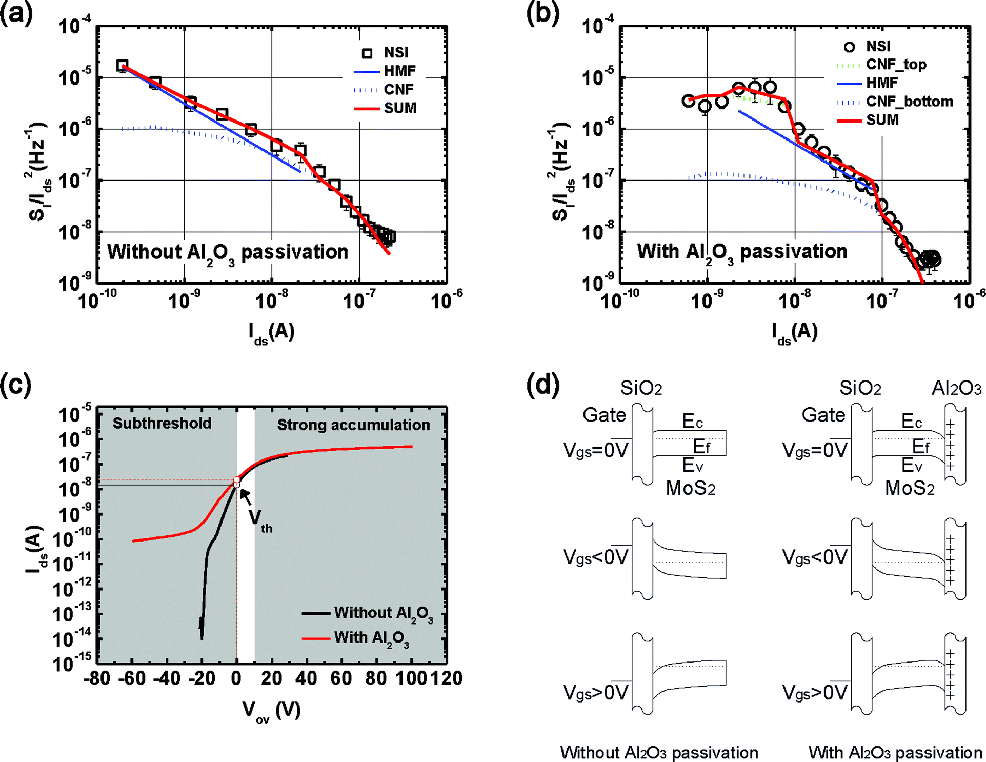 | ||
| Fig. 4 LFN, transfer characteristics, and band diagrams with and without the Al2O3 passivation layer. Normalized drain current spectral density (NSI) from the noise spectra as a function of the drain current (a) without and (b) with the Al2O3 passivation layer. The HMF and CNF models were fitted to the raw data. CNF_top and CNF_bottom refer to the fitted carrier number fluctuation models for the top (near the Al2O3) and the bottom (near the SiO2) surfaces of the channel. The fitting data for the summation of the HMF and CNF models are denoted by “SUM”. (c) Drain current as a function of the gate overdrive voltage, Vov = Vgs − Vth, both with and without the Al2O3 passivation layer. The subthreshold and the strong accumulation regimes are indicated by the gray region. (d) Simplified band diagrams without (left) and with (right) the Al2O3 passivation. The band diagrams at the top, middle, and bottom indicate when the device is as fabricated, with an applied negative gate voltage, and with an applied positive gate voltage, respectively. The conduction and valence band edges of SiO2 and Al2O3 have been omitted for clarity. | ||
At small currents, i.e. the subthreshold regime, there were large discrepancies between the CNF model and the measured SI/Ids2 data shown in Fig. 4(a) and (b). The subthreshold regimes are represented as the transfer characteristics in Fig. 4(c), and as band diagrams in Fig. 4(d). Considering that multilayer MoS2 FETs operate as accumulation-mode transistors, since MoS2 is a natural n-type semiconductor, and that the devices are junctionless transistors, i.e. they have the same doping concentrations in the source, drain, and channel regions, we can expect that the threshold voltages should be less than or equal to the flat-band voltages.46 The enlarged section of the transfer characteristic curve below the threshold voltage without the Al2O3 passivation layer, shown in Fig. 4(c), is consistent with FETs that operate in accumulation-mode and are junctionless. These kinds of “stretched-out” transfer characteristics are typically observed in accumulation-mode and junctionless transistors, and are regarded as the bulk conduction portions.47,48 However, the threshold voltages extracted from the transfer characteristics in this study were larger than the flat band voltages.32 Due to the very small contribution of bulk conduction to the total current, this stretched-out part of the transfer characteristics can be ignored, and the surface conduction channel is important in determining the threshold voltages. If the doping density or the effective channel size of the multilayer MoS2 is small enough, the bulk conduction channel is hard to observe in the transfer characteristics. In this study, the transfer curve shown in Fig. 4(c) suggests a relatively small bulk conduction portion. When the bulk conduction is the dominant current pathway (in the subthreshold regime), there is a possibility that the CNF model may not be appropriate, and that instead, the HMF model may better describe the noise characteristics of the subthreshold regime.
According to the HMF model, the normalized drain current spectral density can be expressed as:16
 | (3) |
 | (4) |
In many reports of noise analyses, it is unclear whether the noise characteristics follow the HMF or CNF model. The HMF model has rarely been introduced to explain the noise characteristics, even in Si MOSFETs. Particularly, the HMF model has been used to describe the noise characteristics of p-MOS buried-channel structures,51 and more recently, Persson et al.52 showed that the HMF and the CNF models could be used to describe the noise properties in the vertical wrap-gated Sn-doped InAs nanowire FETs with the core channel and the surface channel, respectively. In the case of the multilayer MoS2 FET, however, the HMF model is relatively easily observed without the buried-channel structures or any intentional doping and the gate-all-around structures. Even in the case of the relatively thick-multilayer (∼40 nm) MoS2 FET, we confirmed that only the HMF model was fitted all over the operation regime as in Fig. 5. This implies that the influence of the traps in the gate insulator to the conduction is very weak. Recently, Das et al.53 suggested the resistor network model to describe the current distribution in multilayer MoS2 FET based on Thomas–Fermi charge screening and interlayer coupling. According to those results, accumulation charges induced by the back gate bias can be distributed deeply along to the multilayer MoS2 due to the high T–F charge screening length (λ ∼ 7 nm) and the interlayer resistance (Rint) has high value, so the dominant current flow may not occur though the lowest layer of the multilayer MoS2. Once the dominant conduction is far from the gate insulator, the probability arising from the carrier trapping/detrapping in the oxide traps in the gate insulator can be reduced, which is already confirmed by other studies that we have referred to above.51,52 This might be a reason why the HMF model is well fitted instead of the CNF model in the thick-multilayer (∼40 nm) MoS2 FETs in the entire regime. In the case of the 11.3 nm thick-multilayer MoS2 FET, the CNF model could be introduced to describe the noise properties in Fig. 4(a) because the thickness of the MoS2 is relatively small, although the dominant current flow does not occur through the lowest layer. If then, there is still a possibility to introduce the CNF model in the strong accumulation regime. Our results can describe Das et al.'s work,53 but more specific theory about the current flow in 2-D nanomaterials should be studied. Also, using the relatively well-described Si accumulation-mode or junctionless transistor theory to describe the electrical properties of MoS2 FETs should be accompanied.
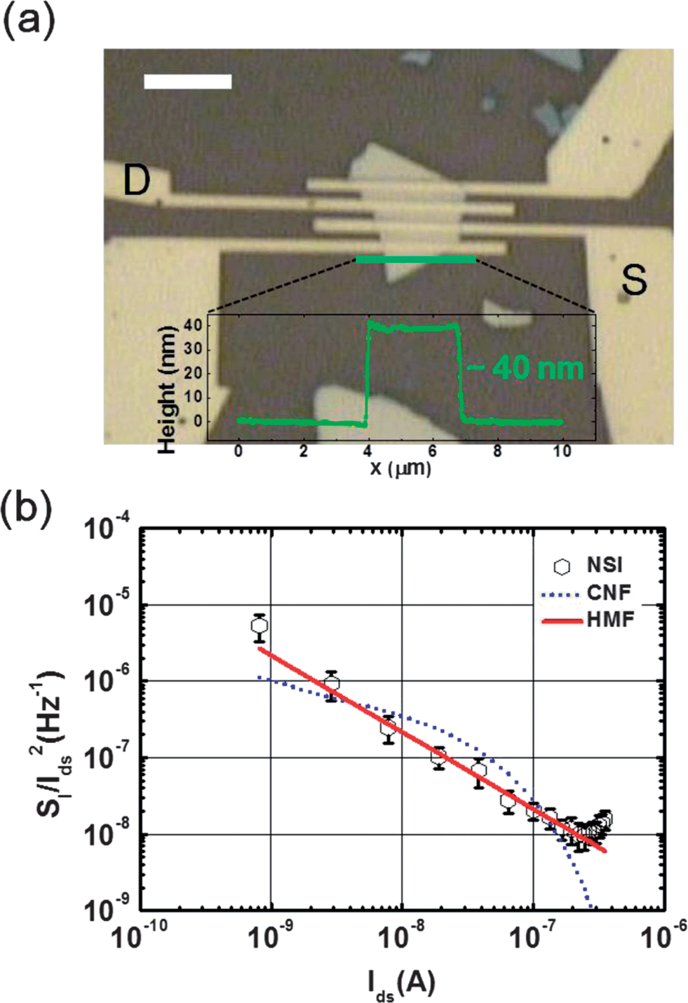 | ||
| Fig. 5 (a) Optical images after the formation of source/drain metal contact on the thick-multilayer MoS2. ‘D’ and ‘S’ represent the drain and the source contact, respectively. Other electrodes were intended for the four probe measurements but were not used in the noise measurements. The scale bar is 5 μm long. The inset shows that the thickness of the MoS2 layer was approximately 40 nm by AFM. (b) Normalized drain current spectral density (NSI) from the noise spectra as a function of the drain current without the Al2O3 passivation layer. Only the HMF model (HMF) was fitted to the raw data. | ||
In the device with the Al2O3 passivation layer (Fig. 4(b)), the HMF model does not adequately fit the SI/Ids2 behavior. In the subthreshold regime, the surface channel near the SiO2 was not the dominant pathway, and instead, bulk conduction and other surface current pathways induced by the Al2O3 passivation were dominant in the noise characteristics. Fig. 4(d) shows the band diagrams with the Al2O3 layer; this indicates the possibility of additional surface channels near the MoS2–Al2O3 interface. By introducing the additional CNF model to fit the data in the subthreshold regime, a good fit was obtained, as shown in Fig. 4(b). This distinct difference between the devices with and without the Al2O3 passivation layer is consistent with the bump in the curve shown in Fig. 3(c), which was attributed to additional surface channels induced by the Al2O3 passivation layer. Considering the high value of the interlayer resistance (Rint),53 the existence of the additional top surface channel induced by the Al2O3 passivation is very convincing. When both of the charges induced by Al2O3 on the topmost layer of the MoS2 and the Rint are high, the conditions are sufficiently satisfied so that the dominant current flow can occur through the topmost layer in the deep subthreshold regime of the multilayer MoS2 FET with the Al2O3 passivation.
If Cox at the top surface channel caused by the Al2O3 layer can be approximated to that of the surface channel induced by the back-gate, the interface trap density for the Al2O3–MoS2 interface can be extracted as Nit = 1.8 × 1012 cm−2 eV−1 from the additional CNF model using eqn (1) and (2). If the Cox is considered to be overestimated owing to the geometrical gate coupling effect, then Nit will be lower according to the Cox2 dependence as in eqn (2); therefore, we can expect Nit ∼ 1011 cm−2 eV−1. This is consistent with the interface trap density (Dit) = 2.4 × 1012 cm−2 eV−1, and Dit = 2.6 × 1011 cm−2 eV−1 for the MoS2–Al2O3 interface in top-gate15 and back-gate11 geometries, calculated using the subthreshold swing, respectively. In addition, Dit in high-k materials has been reported to lie in the range 1011 < Dit < 1012 cm−2 eV−1.18,19,54 If the electrical parameters such as Cox or mobility can be extracted more precisely by using the analytical or numerical solutions, we believe that the noise analyses of the MoS2 FETs can be a more powerful tool to diagnose the interface quality between the high-k dielectric and MoS2.
High-k dielectrics, including Al2O3, HfO2, and ZrO2, are known to retain more fixed charges than SiO2.18,19,39,54 To ensure stable device operation, the effects of these fixed charges on the device characteristics should be studied. Carbon nanotube transistors have been observed to change from p-type to n-type following Al2O3 passivation; this was attributed to fixed charges, with the positive polarity in the Al2O3 leading to electrostatic doping.55,56 Shin et al.57 suggested that there may be a nonuniform distribution of fixed charges in Al2O3. In InGaAs–Al2O3 structures, negative fixed charges may be located near the interface between the Al2O3 and the InGaAs, with positive fixed charges in the Al2O3 away from the interface. This suggests that the total electric field in the MoS2 in our samples may be the sum of the potential due to localized charge distribution near the MoS2–Al2O3 interface and in the bulk part of the Al2O3 layer. Then, the dominant fixed charges can be positive in our case, as shown in Fig. 6, because the bulk part of the Al2O3 layer that we deposited is relatively as large as the 30 nm-thick. It is clear that an additional top surface channel in the multilayer MoS2 transistors is induced by the Al2O3 passivation. The increase in the off-current and the noise characteristics is evidence of this. If those phenomena result from fixed charges in the Al2O3 layer, the electrostatic doping effect may be positive in the case of the multilayer MoS2 transistors reported here.
 | ||
| Fig. 6 Schematic diagrams of the cross-section of the device (a) without and (b) with the Al2O3 passivation layer. In ambient air, gas molecules (mainly oxygen and water) are absorbed on to the MoS2 surface and induce a depletion region. Following the Al2O3 passivation, the gas molecules in ambient air can no longer deplete the multilayer MoS2; however, positive fixed charges in the Al2O3 layer can induce an additional conduction pathway via electrostatic doping at the top of the MoS2 layer. | ||
Conclusions
We have performed LFN characterization of multilayer MoS2 FETs (∼11.3 nm) with and without an Al2O3 passivation layer. In the strong accumulation regime, the carrier number fluctuation (CNF) model associated with trapping/detrapping the charge carriers at the interface was used to describe the noise behavior, both with and without the passivation. The interface trap density at the MoS2–SiO2 interface extracted from the LFN measurements was Nit = 7.2 × 10¹⁰ eV−1 cm−2 without the Al2O3 passivation layer and Nit = 5.5 × 10¹⁰ eV−1 cm−2 with the passivation layer. Those two similar Nit values represented that the accumulation channel induced by the back-gate was not significantly influenced by the passivation layer. The Hooge mobility fluctuation (HMF) model was introduced to describe the electrical properties in terms of bulk conduction in the subthreshold regime. For the thick-MoS2 (∼40 nm) FET, the HMF model was fitted all over the operation regime, ensuring the existence of the bulk conduction in multilayer MoS2. With the addition of the Al2O3 passivation, an additional top surface channel was induced, which led to an increase of the off-current. This change is also apparent in the noise behavior so the additional (CNF) model was successfully introduced when the Al2O3 passivation layer was placed. The trap density at the MoS2–Al2O3 interface was Nit = 1.8 × 10¹² eV−1 cm−2. These results can be a great help to understand the interactions between MoS2 and high-k materials.Acknowledgements
This work was supported by the National Research Foundation of Korea (NRF) funded by the Ministry of Science, ICT and Future Planning (Converging Research Center Program, 2013K000175 and Global Frontier Research Program, No. 2011-0031638).Notes and references
- A. K. Geim, Science, 2009, 324, 1530–1534 CrossRef CAS PubMed.
- M. Y. Han, B. Özyilmaz, Y. Zhang and P. Kim, Phys. Rev. Lett., 2007, 98, 206805 CrossRef.
- D. S. L. Abergel, V. Apalkov, J. Berashevich, K. Ziegler and T. Chakraborty, Adv. Phys., 2010, 59, 261–482 CrossRef CAS.
- M. F. Craciun, S. Russo, M. Yamamoto and S. Tarucha, Nano Today, 2011, 6, 42–60 CrossRef CAS PubMed.
- Nat. Nanotechnol., 2012, 7, 683–683 Search PubMed.
- B. Radisavljevic, A. Radenovic, J. Brivio, V. Giacometti and A. Kis, Nat. Nanotechnol., 2011, 6, 147–150 CrossRef CAS PubMed.
- K. S. Novoselov, D. Jiang, F. Schedin, T. J. Booth, V. V. Khotkevich, S. V. Morozov and A. K. Geim, Proc. Natl. Acad. Sci. U. S. A., 2005, 102, 10451–10453 CrossRef CAS PubMed.
- M. S. Fuhrer and J. Hone, Nat. Nanotechnol., 2013, 8, 146–147 CrossRef CAS PubMed.
- B. Radisavljevic and A. Kis, Nat. Nanotechnol., 2013, 8, 147–148 CrossRef CAS PubMed.
- W. Choi, M. Y. Cho, A. Konar, J. H. Lee, G.-B. Cha, S. C. Hong, S. Kim, J. Kim, D. Jena, J. Joo and S. Kim, Adv. Mater., 2012, 24, 5832–5836 CrossRef CAS PubMed.
- S. Kim, A. Konar, W. S. Hwang, J. H. Lee, J. Lee, J. Yang, C. Jung, H. Kim, J. B. Yoo, J. Y. Choi, Y. W. Jin, S. Y. Lee, D. Jena, W. Choi and K. Kim, Nat. Commun., 2012, 3, 1011 CrossRef PubMed.
- A. Castellanos-Gomez, M. Barkelid, A. M. Goossens, V. E. Calado, H. S. J. van der Zant and G. A. Steele, Nano Lett., 2012, 12, 3187–3192 CrossRef CAS PubMed.
- Y. Liu, H. Nan, X. Wu, W. Pan, W. Wang, J. Bai, W. Zhao, L. Sun, X. Wang and Z. Ni, ACS Nano, 2013, 7, 4202–4209 CrossRef CAS PubMed.
- X. Lu, M. I. B. Utama, J. Zhang, Y. Zhao and Q. Xiong, Nanoscale, 2013, 5, 8904–8908 RSC.
- L. Han and P. D. Ye, IEEE Electron Device Lett., 2012, 33, 546–548 CrossRef.
- G. Ghibaudo, O. Roux, C. Nguyen-Duc, F. Balestra and J. Brini, Phys. Status Solidi A, 1991, 124, 571–581 CrossRef.
- T. Boutchacha, G. Ghibaudo, G. Guégan and T. Skotnicki, Microelectron. Reliab., 1997, 37, 1599–1602 CrossRef.
- M. Bigang, S. P. Devireddy, Z. Celik-Butler, W. Fang, A. Zlotnicka, T. Hsing-Huang and P. J. Tobin, IEEE Trans. Electron Devices, 2004, 51, 1679–1687 CrossRef.
- C. Claeys, E. Simoen, A. Mercha, L. Pantisano and E. Young, J. Electrochem. Soc., 2005, 152, F115–F123 CrossRef CAS PubMed.
- H. Li, G. Lu, Z. Yin, Q. He, H. Li, Q. Zhang and H. Zhang, Small, 2012, 8, 682–686 CrossRef CAS PubMed.
- W. Ying Ying, G. Ren Xi, N. Zhen Hua, H. Hui, G. Shu Peng, Y. Huan Ping, C. Chun Xiao and Y. Ting, Nanotechnology, 2012, 23, 495713 CrossRef PubMed.
- M.-K. Joo, P. Kang, Y. Kim, G.-T. Kim and S. Kim, Rev. Sci. Instrum., 2011, 82, 034702 CrossRef PubMed.
- O. L. Jeong, C. Park, K. Ju-Jin, K. Jinhee, P. Jong Wan and Y. Kyung-Hwa, J. Phys. D: Appl. Phys., 2000, 33, 1953 CrossRef.
- W. Yunsung, S. D. Georg and R. Siegmar, Nanotechnology, 2007, 18, 095203 CrossRef.
- D. J. Late, B. Liu, H. S. S. R. Matte, V. P. Dravid and C. N. R. Rao, ACS Nano, 2012, 6, 5635–5641 CrossRef CAS PubMed.
- H. Qiu, L. Pan, Z. Yao, J. Li, Y. Shi and X. Wang, Appl. Phys. Lett., 2012, 100, 123104 CrossRef.
- F. K. Perkins, A. L. Friedman, E. Cobas, P. M. Campbell, G. G. Jernigan and B. T. Jonker, Nano Lett., 2013, 13, 668–673 CrossRef CAS PubMed.
- P. Woanseo, P. Juhun, J. Jingon, L. Hyungwoo, J. Hyunhak, C. Kyungjune, H. Seunghun and L. Takhee, Nanotechnology, 2013, 24, 095202 CrossRef PubMed.
- C.-W. Lee, I. Ferain, A. Afzalian, R. Yan, N. D. Akhavan, P. Razavi and J.-P. Colinge, Solid-State Electron., 2010, 54, 97–103 CrossRef CAS PubMed.
- H. Wang, L. Yu, Y.-H. Lee, Y. Shi, A. Hsu, M. L. Chin, L.-J. Li, M. Dubey, J. Kong and T. Palacios, Nano Lett., 2012, 12, 4674–4680 CrossRef CAS PubMed.
- D. Jena and A. Konar, Phys. Rev. Lett., 2007, 98, 136805 CrossRef.
- S. Das, H.-Y. Chen, A. V. Penumatcha and J. Appenzeller, Nano Lett., 2012, 13, 100–105 CrossRef PubMed.
- K. Nagashio, T. Nishimura, K. Kita and A. Toriumi, Appl. Phys. Express, 2009, 2, 025003 CrossRef.
- S.-L. Li, K. Wakabayashi, Y. Xu, S. Nakaharai, K. Komatsu, W.-W. Li, Y.-F. Lin, A. Aparecido-Ferreira and K. Tsukagoshi, Nano Lett., 2013, 13, 3546–3552 CrossRef CAS PubMed.
- G. Liu, W. Stillman, S. Rumyantsev, Q. Shao, M. Shur and A. A. Balandin, Appl. Phys. Lett., 2009, 95, 033103 CrossRef.
- A. N. Pal and A. Ghosh, Appl. Phys. Lett., 2009, 95, 082105 CrossRef.
- S. Qinghui, L. Guanxiong, D. Teweldebrhan, A. A. Balandin, S. Rumyantsev, M. S. Shur and Y. Dong, IEEE Electron Device Lett., 2009, 30, 288–290 CrossRef.
- Y.-M. Lin, J. Appenzeller, J. Knoch, Z. Chen and P. Avouris, Nano Lett., 2006, 6, 930–936 CrossRef CAS PubMed.
- U. J. Kim, K. H. Kim, K. T. Kim, Y.-S. Min and W. Park, Nanotechnology, 2008, 19, 285705 CrossRef PubMed.
- W. Wang, H. D. Xiong, M. D. Edelstein, D. Gundlach, J. S. Suehle, C. A. Richter, W.-K. Hong and T. Lee, J. Appl. Phys., 2007, 101, 044313 CrossRef.
- J. Lee, B.-Y. Yu, C. H. Lee, G.-C. Yi, S. H. Son, G.-T. Kim and G. Ghibaudo, Phys. E., 2008, 40, 2147–2149 CrossRef CAS PubMed.
- S. Ju, P. Chen, C. Zhou, Y.-g. Ha, A. Facchetti, T. J. Marks, S. K. Kim, S. Mohammadi and D. B. Janes, Appl. Phys. Lett., 2008, 92, 243120 CrossRef.
- J. Huh, M.-K. Joo, D. Jang, J.-H. Lee and G. T. Kim, J. Mater. Chem., 2012, 22, 24012–24016 RSC.
- M.-K. Joo, J. Huh, M. Mouis, S. J. Park, D.-Y. Jeon, D. Jang, J.-H. Lee, G.-T. Kim and G. Ghibaudo, Appl. Phys. Lett., 2013, 102, 053114 CrossRef.
- M. Z. Hossain, S. L. Rumyantsev, K. M. F. Shahil, D. Teweldebrhan, M. Shur and A. A. Balandin, ACS Nano, 2011, 5, 2657–2663 CrossRef CAS PubMed.
- J. P. Colinge, A. Kranti, R. Yan, C. W. Lee, I. Ferain, R. Yu, N. Dehdashti Akhavan and P. Razavi, Solid-State Electron., 2011, 65–66, 33–37 CrossRef CAS PubMed.
- J. P. Colinge, IEEE Trans. Electron Devices, 1990, 37, 718–723 CrossRef.
- D.-Y. Jeon, S. J. Park, M. Mouis, S. Barraud, G.-T. Kim and G. Ghibaudo, Solid-State Electron., 2013, 80, 135–141 CrossRef CAS PubMed.
- D.-Y. Jeon, S. J. Park, M. Mouis, S. Barraud, G.-T. Kim and G. Ghibaudo, Solid-State Electron., 2013, 81, 101–104 CrossRef CAS PubMed.
- S. Liang-Yu, L. Huang-Kai, H. Chia-Chin and H. JianJang, J. Disp. Technol., 2012, 8, 695–698 CrossRef.
- G. Ghibaudo and J. Chroboczek, Solid-State Electron., 2002, 46, 393–398 CrossRef CAS.
- K.-M. Persson, B. G. Malm and L.-E. Wernersson, Appl. Phys. Lett., 2013, 103, 033508 CrossRef.
- S. Das and J. Appenzeller, Nano Lett., 2013, 13, 3396–3402 CrossRef CAS PubMed.
- G.-W. Lee, J.-H. Lee, H.-W. Lee, M.-K. Park, D.-G. Kang and H.-K. Youn, Appl. Phys. Lett., 2002, 81, 2050–2052 CrossRef CAS.
- N. Moriyama, Y. Ohno, T. Kitamura, S. Kishimoto and T. Mizutani, Nanotechnology, 2010, 21, 165201 CrossRef CAS PubMed.
- U. J. Kim, H. B. Son, E. H. Lee, J. M. Kim, S. C. Min and W. Park, Appl. Phys. Lett., 2010, 97, 032117 CrossRef.
- B. Shin, J. R. Weber, R. D. Long, P. K. Hurley, C. G. V. d. Walle and P. C. McIntyre, Appl. Phys. Lett., 2010, 96, 152908 CrossRef.
Footnote |
| † Electronic supplementary information (ESI) available: The effects of thermal annealing, the change of the off-current, the numerically calculated gate capacitances, the raw LFN data, and specific band diagrams are described in detail here. See DOI: 10.1039/c3nr04218a |
| This journal is © The Royal Society of Chemistry 2014 |