Few layer graphene to graphitic films: infrared photoconductive versus bolometric response†
Narendra
Kurra
,
Venkata Srinu
Bhadram
,
Chandrabhas
Narayana
and
Giridhar U.
Kulkarni
*
Chemistry & Physics of Materials Unit and DST Unit on Nanoscience, Jawaharlal Nehru Centre for Advanced Scientific Research, Jakkur P.O., Bangalore 560 064, India. E-mail: kulkarni@jncasr.ac.in; Fax: +91 (80)22082766; Tel: +91 (80)22082814
First published on 6th November 2012
Abstract
We report a comparative study of the performance of infrared (IR) photoconductive and bolometric detectors fabricated from few layer graphene (FLG) to graphitic films obtained by different methods. FLG films grown directly on insulating substrates with the aid of residual hydrocarbons and polymethylmethacrylate (PMMA) carbon sources show an IR photoresponse of 73% which is far higher compared to the FLG films (6–14%) obtained by CVD and Scotch tape methods. The photoconductive nature of FLG films is due to generation of photoexcited charge carriers. On the other hand, the photoresponse of the bulk graphitic films is bolometric in nature where the resistance changes are due to thermal effects. The IR photoresponse from these graphitic films is correlated with the Raman peak intensities which are very sensitive to the nature of the FLG.
1 Introduction
Graphene, a two-dimensional crystalline allotrope of carbon, exhibits unique and extra-ordinary electronic,1–3 thermal,4 mechanical5 and optoelectronic properties.6–8 It has been employed as a transparent conductor in solar cell applications.9–11 Graphene absorbs over a wide range of electromagnetic radiation from infrared (IR) to terahertz, due to large strength of intraband and interband transitions involving the valence and conduction bands.9,12 Due to high mobility of charge carriers in graphene, single and also few layer graphene have been exploited in fabricating ultrafast photodetectors.13 In addition, phototransistors have been fabricated using graphene nanoribbons.14 Different studies have demonstrated the origin of photocurrent generation by studying the role of interfaces which mainly include single and bilayer regions,15 edge regions16 and near metallic contacts.17 The photoresponse from graphene based p–n junctions,18,19 ultrafast hot carrier effects in graphene, electron–hole separation near the graphene–metal contacts and generation of photocurrents have been investigated.20–22 Position dependent photocurrents in the reduced graphene oxide (RGO) films have demonstrated the role of carbon–metal interfaces.23–25 Hybrid structures of Au, ZnO and PbS quantum dots in combination with graphene have been fabricated to enhance the performance of phototransistors.26–29 Recently, dual-gated bilayer graphene has been employed to fabricate a hot-electron bolometer.30 In bolometric response, the resistance changes are due to thermal effects but not due to photoexcited holes and electrons.31 Graphene based superconducting tunnel junctions showing bolometric response have been projected in ultrasensitive bolometry and calorimetry applications useful in fields such as astronomy and quantum information.32,33 In general, photoconductive and bolometric responses are dependent on the material properties such as absorption coefficient, thermal conductivity along with the nature of the material–electrode interface.Graphene for such purposes is usually obtained via mechanical exfoliation,13 epitaxially grown films,34 chemical vapor deposited graphene26 and reduced graphene oxide films.23–25 However, there is no systematic study on the photoresponse behavior of the graphene obtained by various methods and also relative to the bulk graphite. Here, in this study, we report the IR photoconductive and bolometric responses from the FLG and bulk graphite. We have grown FLG films directly on insulating substrates (quartz, SiO2) by annealing sacrificial Ni thin films in the ambience of residual hydrocarbons in a vacuum chamber. Thus the obtained FLG films showed a maximum photoresponse of 73%. The IR photoresponses of the FLG films obtained from PMMA as a carbon source and also the transferred FLG films (CVD grown graphene and from mechanical exfoliation) have been compared. The IR response of the bulk graphitic films, on the other hand, was bolometric in nature where the change in the resistance is due to the thermal effects. Thus, by controlling the thickness and crystallite size of the graphene layers, one can tune the IR photoresponse from the photoconductive to bolometric regime.
2 Results and discussion
Fig. 1(a) illustrates the growth of few layer graphene (FLG) on an insulating SiO2 substrate with the aid of residual hydrocarbons abundant in the vacuum chamber. The vacuum chamber used in this study is pumped by an oil-based diffusion pump (at a base pressure of 10−5 Torr) which is backed by a rotary pump. These pumps liberate volatile hydrocarbon species into the vacuum chamber which get adsorbed onto the substrate surface. Following vacuum annealing of the SiO2/Si substrates at 1050 °C covered with thin Ni film (thickness, 30 nm) deposited by physical vapor deposition, the adsorbed hydrocarbon species transformed into crystallites of graphene as evidenced from Raman analysis (see Fig. 1(b) and S1, ESI†). The Raman spectrum showed characteristic G and 2D bands at 1585 and 2690 cm−1 respectively (see Fig. S1, ESI†). Thus, Ni acts as a catalyst layer to induce the growth of crystalline sp2 carbon from the volatile residual hydrocarbons present in the vacuum chamber.35–37 The Raman spectrum of the graphitic deposits obtained after etching away the Ni layer consists of D (1350 cm−1) and G (1585 cm−1) bands (spectrum 1, Fig. 1(b)) with line widths of 85 and 40 cm−1 respectively (ID/IG ratio of ∼0.50). The 2D band appeared as a single peak (position ∼ 2690 cm−1) with a line width of 70 cm−1. The IG/I2D ratio was found to be 1.5–2, indicating that the obtained graphene is of few layers.38 Due to high solubility of carbon in Ni at the annealing temperature, the carbon atoms can diffuse through the Ni lattice and precipitate as graphene on the bottom SiO2 surface (see the schematic in Fig. 1(a)).39,40 Without the Ni overlayer, the carbon species hardly undergoes a change. The spectrum recorded from the SiO2 region (without Ni layer) consists of only broad D and G bands with the 2D band being absent, indicating the amorphous nature of carbon unlike that from the Ni etched region (see spectrum 2, Fig. 1(b) and the optical micrograph in the inset).41,42 AFM topography in Fig. 1(c) shows interconnected graphene features along with some residual Ni crystallites, which could not get etched away; perhaps they have passivated with the graphene layers. | ||
| Fig. 1 (a) Schematic illustration of direct growth of FLG on SiO2/Si over large area using residual hydrocarbons in the vacuum chamber. (b) Raman spectra of the precipitated FLG and amorphous carbon from Ni (spectrum 1) and SiO2 (spectrum 2) regions respectively. The inset shows the optical micrograph of Ni and SiO2 regions. (c) AFM topography of the FLG features on the SiO2 surface. | ||
The AFM topography along with the z-profiles for the FLG and graphitic samples are shown in Fig. S2.† The typical thickness of FLG samples is in the range of 1–3 nm and the bulk graphitic samples of 0.6 and 18 μm are used for the photoresponse studies. The mobility values of the FLG samples are obtained from the field effect transistor (FET) measurements in which we have used SiO2 (300 nm) as a bottom gate dielectric. All the FLG samples showed p-type behavior and hole mobilities are in the range of 550 to 8 cm2 V−1 s−1 (see Fig. S3†). The p-type doping is due to unintentional doping by the ambient water and oxygen molecules supported by the bottom SiO2 surface. The defects present in the FLG may also support the adsorption of water molecules leading to the p-type behavior.39,40,43
The photoresponse behavior of FLG derived from residual hydrocarbons (RHC–FLG) has been examined under the IR source (Fig. 2). From the I–V characteristics shown in Fig. 2(a), we see that the current in the circuit increases under IR illumination (red curve) relative to that obtained without illumination (black curve). This can be attributed to the generation of photoexcited charge carriers resulting in the enhanced photocurrent. When monitored with time (Fig. 2(b)), the base resistance was found to decrease from ∼30 to 9 kΩ within ∼70 s under the IR beam (power, 20 mW cm−2). The reduction in the resistance value is mainly due to the generation of photoexcited charge carriers and not due to photocurrent. The latter, which arises due to excitation of charge carriers near the metal–graphene interface and their separation by the built-in electric field or local thermal fields, is typically of the order of nanoamperes. The dependence of resistance on photoexcited carrier density is given as ΔR = (L/W)(1/eμ)(1/Δn), where ΔR is the change in the resistance due to IR illumination, L and W are length and widths of the FLG, e is the electron charge, μ is the mobility and Δn is the change in the charge carrier concentration due to IR illumination. After substituting the values, we have seen a change in the carrier concentration of 3.7 × 1013 cm−2 for a given change of resistance of 21 kΩ in the FLG sample (equilibrium charge carrier concentration ∼ 2.6 × 1013 cm−2 at room temperature). The resistance increased to nearly its original value from the moment the IR beam was turned off (see Fig. 2(b)). The photoresponse estimated based on the resistance values is 73%, which qualifies RHC–FLG as an IR detector (see Fig. S4, ESI†). It may be noted that the photoresponse is lower than that from the graphene thin films derived from RGO.24 In the present study, the typical thickness of FLG is of the order of 1–3 nm (see Fig. S2†), i.e., ∼4 orders of magnitude less, compared to that in ref. 24, and correspondingly, its IR absorption is also less. The observed large photocurrent responses up to 1800% (in ref. 24) at the metal–RGO interface have been attributed to the built-in electric fields and optically generated temperature gradients. The photoresponse has increased from 150% to 1800% with increasing laser power of 40 to 335 mW respectively.24 Ghosh et al. have explained the enhanced photocurrents up to 193% for the reduced graphene oxide films (0.6 μm thick) using a Schottky barrier model.25 Thus, the magnitude of photoresponse depends on the thickness of the graphene layers, graphene–metal interfaces and the laser power.24,25
 | ||
| Fig. 2 (a) Two probe I–V characteristics of the FLG films (derived from the residual hydrocarbons) in the dark (black curve) and illuminated by an IR laser (1064 nm) (red curve). (b) Plot showing the photoresponse behavior towards the IR beam. (c) Few cycles of response, and (d) the response with varying IR beam energies. The inset shows a plot of change in resistance versus laser beam energy. “On” is indicated with green circles which indicate the time when the IR beam is turned on and at that moment the resistance starts decreasing. “Off” is indicated with red circles, pointing the time when the IR beam was turned off. | ||
The time constants for the growth and decay of the photocurrent induced by the IR laser beam were calculated after fitting with exponential functions (see Fig. S5, ESI†) and they were found to be 41 and 50 seconds respectively. The time response is much slower for our graphene films as compared with the crystalline graphene where the time response is of the order of picoseconds.13 The slower response times can be attributed to the presence of disorder and interfaces in the graphene films. The scattering of the charge carriers by the traps and boundaries can lead to a slower response. The stability of the circuit has been tested by turning the IR laser source on and off repeatedly for four cycles (Fig. 2(c)). Accordingly, the changes in resistance were consistent in each cycle. There is a gradual decrease in the resistance with increasing the laser power from 10 to 40 mW cm−2 (Fig. 2(d)). The change in the resistance is slightly non-linear (see the inset in Fig. 2(d)). In this study, we have used a shadow mask technique for the deposition of the electrodes which is a ‘clean’ method unlike photolithography and electron beam lithography, which leave residues of resists behind and may influence the optoelectronic properties of FLG. The IR photoresponse of the RHC–FLG deposited on the quartz and sapphire substrates is shown in Fig. S6, ESI.† The varied photoresponse of RHC–FLG films can be attributed to the number of defects which is tunable through annealing temperature and annealing time.
In order to examine the photoresponse behavior of the FLG obtained by other methods, we chose PMMA as a solid carbon source, which was transformed into FLG by thermal treatment in the presence of the Ni catalyst layer (see Experimental section for details). The Raman spectrum recorded after washing away the Ni catalyst layer (Fig. 3(a)) showed D, G and 2D bands at ∼1350, 1587 and 2678 cm−1 respectively with ID/IG and IG/I2D ratios of 0.5 and 2.5, respectively. The AFM topography of PMMA–FLG shows graphene sheets interconnected with each other over a large area (see the inset in Fig. 3(a)), similar to that observed with RHC–FLG (Fig. 1(c)).36,37 The PMMA–FLG film with a base resistance of 2.16 kΩ showed a photoresponse of 21% and the temporal behavior is shown for four cycles (see Fig. 3(b)). Similarly, the photoresponse of 16% was observed for the PMMA–FLG film with a base resistance of 1.75 kΩ (see Fig. 3(c)). It appears that the PMMA–FLG films are more conductive than the RHC–FLG films but the former exhibited lower photoresponse as compared to the latter.
 | ||
| Fig. 3 (a) Raman spectrum of the FLG derived from PMMA (FLG–PMMA), and the inset shows the AFM topography of the PMMA–FLG film on the SiO2/Si surface. (b and c) IR photoresponse of two different circuits of PMMA–FLG. The inset is the optical micrograph of the circuit with Au contact pads. | ||
The IR photoresponse properties of the FLG obtained by CVD and Scotch tape methods are illustrated in Fig. 4. We observed a decrease in the resistance after illuminating with the IR laser beam from 276 to 236 Ω corresponding to a photoresponse of 14% (see Fig. 4(a)). This value is comparable to that obtained with the PMMA–FLG films (see Fig. 3). The temporal IR photoresponse of the CVD-graphene is shown in Fig. 4(b) for a few cycles. It is observed that the final resistance value (Rf) does not return to the original base resistance (Rb) after turning off the IR beam which may be due to non-equilibration of photoexcited charge carriers. Another FLG circuit was made from the FLG ribbon obtained by a Scotch tape technique which is also exhibiting a photoconductive response. The resistance of the FLG ribbon is changing from 1.54 to 1.44 kΩ after turning on the IR beam, and the IR response was only 6% (see Fig. 4(c) and (d)). The final resistance value (Rf) is found to be higher than the original base resistance (Rb) after turning off the IR beam which is due to the heating effect.
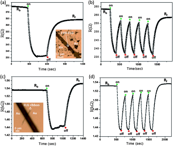 | ||
| Fig. 4 (a and b) IR photoresponse of the FLG transferred onto the SiO2 surface (CVD grown graphene film on the Ni surface). The inset shows the optical micrograph of FLG between two Au contact pads. (c and d) IR photoresponse of the FLG obtained by a Scotch tape method. The inset shows the optical micrograph of the circuit containing FLG across 6 μm Au contact pads. | ||
Fig. 5 shows the IR photoresponse from the bulk graphitic films. The base resistance of the sample is found to be 15.8 Ω which is increased up to 18.2 Ω after illuminating with the IR beam (see Fig. 5(a)). The increase in the resistance should be due to thermal energy imparted to the carbon lattice upon illuminating with the IR beam. A similar photoresponse behavior is observed for the carbon fibre which is also graphitic (many layers) in nature (see Fig. 5(b)). The photoresponses are found to be 12 and 10% for bulk graphite and carbon fibre samples respectively. The time constants for the rise and fall of the resistance for the graphite sample are found to be ∼21 and ∼31 seconds respectively (see Fig. S7†). The response time is found to be rather high compared to that observed in suspended SWNT films which is of the order of 50 ms.31 Typically, the response time of a bolometer is limited by the ratio, τ = C/G where C is the heat capacity and G is the thermal conductance. It is obvious that the low thermal conductance and low heat capacity can minimize the response time. In the present study, the response was measured under ambient conditions giving rise to a high value of the response time. In the case of bulk graphite, the photoexcited charge carriers recombine in an ultra-fast (time scale of pico to femto seconds) manner which is a non-radiative decay producing heat in the graphite lattice. Thus, the absorbed IR radiation has transformed into heat leading to the temperature rise in the graphite lattice. The change in the resistance can be equated with the temperature change as, ΔR = (dR/dT)ΔT, where the temperature coefficient of resistance (dR/dT) from Fig. 7(b) is estimated to be 0.0165 Ω K−1 and ΔR ∼ 2.45 Ω is found from Fig. 5(a). Substituting these values in the above equation, ΔT is found to be ∼150 °C (laser power of 20 mW cm−2). This way, the bolometric response can be linked to the temperature dependent resistance variation.
 | ||
| Fig. 5 (a) Temporal photoresponse from the bulk graphite which is bolometric in nature with %R ∼12%. The inset shows the optical micrograph of the HOPG piece between two Au contact pads. (b) The IR photoresponse from carbon fibre, cycles showing the increase and decrease in the resistance with respect to turning on and off of the IR beam (%R = 10%). Optical micrograph shows the carbon fibre circuit between Au contacts. | ||
In graphitic carbon, IR radiation causes intraband transitions as well as lattice heating, which in terms of electrical transport have opposite effects. Under an applied bias, the intraband transitions lead to photogenerated carriers which in turn increase the conductance while heating induced by the radiation increases the local temperature and hence the resistance due to a reduced mean free path of charge carriers (bolometric effect). The relative influence of these two effects on electrical transport depends on the ‘thickness’ of the graphitic carbon and accordingly, the IR response can be positive or negative. As the Raman intensities may be taken to determine the ‘thickness’ and the nature of the carbon, the IR response from the various samples studied may be correlated with the I2D/IG and ID/IG ratios as shown in the plot of Fig. 6. In the case of bulk graphitic samples (HOPG and C-fibre), whose I2D/IG ratio is found to be ∼0.31 (see circles 1 and 2, Fig. 6(a)), the IR response is bolometric (negative) in nature (%R, 10–12%). Clearly, the thermal effects overcome the photoexcitation events due to high IR absorbance of the bulk graphitic species. Those from the CVD and the Scotch tape methods exhibit a similar but positive response (%R, 6–14%) as the I2D/IG value increases (see circles 3 and 4, Fig. 6(a)), typical of FLGs. The IR response remains nearly steady for the FLGs derived from PMMA although the I2D/IG value is relatively higher (up to 0.39). In this ‘thickness’ regime, the two opposing effects seem to balance each other! As I2D/IG further increases as in the case of FLGs from residual hydrocarbons (circles 7 and 8, Fig. 6(a)), the photoconductive nature takes over the bolometric behavior resulting in higher IR response (21% to 73%). Besides the number of layers, the presence of defects in the graphitic films can also influence the photoresponse (Fig. 6(b)). A defect is essentially a scattering center contributing to increased electrical resistance. It is possible that the IR absorption can thermally activate the charge carriers to overcome the defect barriers giving rise to a higher photoresponse. Thus, the presence of defects, in a way, diverts part of the thermal energy away from the bolometric process to photocurrent. The variation of %R with ID/IG (Fig. 6(b)) is therefore quite striking and supports this view. It is noteworthy that the FLG with in-built defects is more like a self-doped system in contrast to graphene doped externally by metal or semiconductor nanoparticles in order to tune its photoresponse properties.26–29
 | ||
| Fig. 6 (a and b) IR photoresponse of the FLG and graphitic films with respect to I2D/IG and ID/IG ratios respectively. Circles represent different FLG and graphitic samples (1, 2-bulk graphite; 3, 4 – transferred graphene by Scotch tape and CVD; 5, 6 – PMMA–FLG; 7, 8 – RHC–FLG). | ||
Based on the observed photoresponse from FLG and graphitic samples, photoconductive and bolometric behaviours can be explained using a schematic band level diagram shown in Fig. S8, ESI.† The FLG obtained by Scotch tape and CVD methods is shown to have a lower number of localised defect states and accordingly, the change in the current (occupancy above EF) is not significantly different after IR irradiation (Fig. S8(a), ESI†). This is closer to being a bolometric than a photoconductive system. The extreme case is bulk graphite which exhibits only bolometric behaviour. The RHC–FLG, on the other hand (Fig. S8(b), ESI†) may be represented by a discretised band diagram endowed with a large number of localised defect states. In this scenario, the current is less due to limited number of charge carriers. While the nature of conversion from photon to current is unclear,27 it is likely that the defects aid the dissociation of excitons (produced by IR irradiation) into free carriers which can cross the defect potential barrier due to thermal energy leading to enhanced photoconductive response.25 In order to gain further insight into the interplay between charge trapping and recombination processes, we have carried out measurements on temperature dependent resistance variation, with and without IR illumination (see Fig. 7). The RHC–FLG showed a decrease in the resistance with temperature (negative dR/dT) and the HOPG sample showed an opposite behavior (positive dR/dT) (see Fig. 7(a) and (b)). Interestingly, the photoresponse (ΔR/R(300 K)) is found to vary nearly linear with the temperature and higher photoresponse is observed at lower temperatures (compare %R ∼ 50% at 100 K with %R ∼ 10% at 400 K in Fig. 7(c)). It is clear that the recombination rates are higher at higher temperatures leading to the diminished photoresponse. But at lower temperatures due to low recombination rates and enhanced trapping, the photoresponse is higher.44,45 A similar kind of temperature dependent photoconductive effects was observed in the case of disordered carbon aerogel systems.46 The bolometric response showed weak temperature dependence as shown in Fig. 7(d) with a variation of 3% in the temperature range of 80–470 K. This could be attributed to the small change in the resistance with temperature [R(80 K)/R(470 K) = 0.86].31
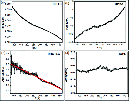 | ||
| Fig. 7 Temperature dependent resistance of RHC–FLG (a) and HOPG (b) with negative and positive temperature coefficients of resistance respectively. (c and d) Photoresponse of the RHC–FLG and HOPG samples with the temperature respectively. | ||
Photoconductive effects in a given system are guided by the interplay between trapping and recombination centers. Defect levels in a system can either act as trapping sites which assist the excitation of the electron into the conduction band or as recombination sites for the holes as it is easier to capture the electron into these levels and release the hole into the valence band. Trapping is a one step process whereas recombination is a two-step process. Trapping centers increase the photoresponse while the recombination centers decrease the photoresponse.
The mutual cooperation of trapping and recombination centers and their influence on the carrier mobility (lifetime) depends on the wavelength and intensity of illumination as well as on the temperature. The carrier recombination at the defect sites plays a dominant role in determining the carrier transport mechanism at different temperatures. Thus, the temperature dependent photoconductive effects are quite complicated to understand. A modeling of the temperature dependent photoconductive effects may deserve a separate study requiring information about the temperature dependent mobility of the charge carriers which are influenced by the trapping and the recombination centers in order to correlate with the observed photoresponse.44,45
3 Conclusions
We have compared the IR photoresponse of FLG and bulk graphitic films obtained by different methods. FLG films obtained through a residual hydrocarbon source exhibited photoconductive response up to 73% due to generation of photoexcited charge carriers after illuminating with the IR beam. The FLG films obtained by CVD and Scotch tape methods showed a typical photoresponse of 6–12%. On the other hand, the photoresponse of the bulk graphitic films is bolometric in nature where the resistance changes are due to thermal effects. Thus, by controlling the thickness and defects of the graphitic films, it is possible to fabricate IR based photoconductive and bolometric detectors. The Raman results clearly elucidate the role of defects in the tunability of the IR response of the FLGs.4 Experimental section
SiO2 (300 nm)/Si substrates were cleaned by sonicating in acetone and isopropanol followed by a rinse in double distilled water for 2 minutes. A Ni catalyst layer (30 nm) was deposited onto SiO2/Si substrates by physical vapor deposition (PVD) at a chamber pressure of 6 × 10⁻⁶ Torr. At this vacuum, the substrate surface gets covered with adsorbed residual hydrocarbons (1 monolayer) within one second.46 Vacuum annealing (P = 2 × 10⁻⁵ Torr) was carried out in the range of 950–1050 °C for 15 minutes. The steps involved in the formation of graphene films from the residual hydrocarbons are shown in Fig. 1(a). For the sake of comparison, other sources of graphene were also tried out. A 2 wt% of PMMA (molecular weight ∼ 996 kDa) was spin coated onto the SiO2 surface at a spin speed of 5000 rpm for 60 s to form a thin film (20 nm). It was subjected to similar heat treatment as done for the residual hydrocarbons resulted in the formation of FLG. This is similar to the formation of FLG from the solid carbon sources. In another experiment, a CVD grown graphene on Ni (Graphene Supermarket, Germany) was transferred onto the SiO2 surface by an electrochemical delamination method.47 Mechanically peeled graphene from HOPG (NT-MDT, mosaic spread ∼0.8°) using the Scotch tape technique also served as a source of FLG in another experiment. The Scotch tape containing flakes of graphene was stamped against a SiO2/Si surface followed by cleaning in hot acetone.2 Raman spectra were recorded at different stages on various graphene samples in the backscattering geometry using a 532 nm excitation from a diode pumped frequency doubled Nd:YAG solid state laser (model GDLM-5015L, Photop Swutech, China) and a custom-built Raman spectrometer equipped with a SPEX TRIAX 550 monochromator and a liquid nitrogen cooled CCD detector (Spectrum One with CCD3000 controller, ISA Jobin Yvon).48 AFM imaging was done on a diInnova SPM (Veeco, USA) using Si probes (model, RTESPA, spring constant 40 N m−1) in tapping mode. The samples of graphene have also been examined under an optical microscope (Laben, India). A 60 nm thick Au film was deposited onto the SiO2/Si substrate by PVD (Hind Hivac, Bangalore) while using a carbon fiber (diameter, 6 μm) as a shadow mask which defined the two contact electrodes for the graphene sample produced from the residual hydrocarbons. For photoresponse measurements, a Nd:YAG laser with a wavelength of 1064 nm (Quanta-Ray GCR-170, Spectra-Physics, USA) was used as an IR source with a maximum power output of 50 mW cm−2. The resistance before and after illuminating with the IR laser was monitored using a digital multimeter (TestLink, India) with computer control. The resistance measurements are done by applying a constant bias of 10 mV. All our measurements have been carried out maintaining similar device configurations. Transistor characteristics were recorded using a Keithley-4200 semiconductor characterization system at room temperature. Temperature dependent resistance measurements were done using a cooling/heating stage (Linkam THMS 600) equipped with a temperature controller (Linkam TMS 94) interfaced with the Keithley 236 source and measure unit.Acknowledgements
The authors thank Professor C. N. R. Rao, FRS for his encouragement. Support from the Department of Science and Technology, Government of India is gratefully acknowledged. NK and VSB acknowledge CSIR for funding. The authors thank Veeco India Nanotechnology Laboratory at JNCASR for the AFM facility. GUK acknowledges the Sheikh Saqr Senior Fellowship.Notes and references
- A. K. Geim and K. S. Novoselov, Nat. Mater., 2007, 6, 183 CrossRef CAS.
- K. S. Novoselov, A. K. Geim, S. V. Morozov, D. Jiang, Y. Zhang, S. V. Dubonos, I. V. Grigorieva and A. A. Firsov, Science, 2004, 306, 666 CrossRef CAS.
- K. S. Novoselov, Z. Jiang, Y. Zhang, S. V. Morozov, H. L. Stormer, U. Zeitler, J. C. Maan, G. S. Boebinger, P. Kim and A. K. Geim, Science, 2007, 315, 1379 CrossRef CAS.
- A. A. Balandin, S. Ghosh, W. Bao, I. Calizo, D. Teweldebrhan, F. Miao and C. N. Lau, Nano Lett., 2008, 8, 902 CrossRef CAS.
- C. Lee, X. Wei, J. W. Kysar and J. Hone, Science, 2008, 321, 385 CrossRef CAS.
- F. Bonaccorso, Z. Sun, T. Hasan and A. C. Ferrari, Nat. Photonics., 2010, 4, 611 CrossRef CAS.
- Q. Bao and K. P. Loh, ACS Nano, 2012, 6, 3677 CrossRef CAS.
- P. Avouris, Nano Lett., 2010, 10, 4285 CrossRef CAS.
- R. R. Nair, P. Blake, A. N. Grigorenko, K. S. Novoselov, T. J. Booth, T. Stauber, N. M. R. Peres and A. K. Geim, Science, 2008, 320, 1308 CrossRef CAS.
- G. Eda, G. Fanchini and M. Chhowalla, Nat. Nanotechnol., 2008, 3, 270 CrossRef CAS.
- H. Bi, F. Huang, J. Liang, X. Xie and M. Jiang, Adv. Mater., 2011, 23, 3202 CrossRef CAS.
- F. Wang, Y. Zhang, C. Tian, C. Girit, A. Zettl, M. Crommie and Y. R. Shen, Science, 2008, 320, 206 CrossRef CAS.
- F. Xia, T. Mueller, Y.-m. Lin, A. Valdes-Garcia and P. Avouris, Nat. Nanotechnol., 2009, 4, 839 CrossRef CAS.
- V. Ryzhii, V. Mitin, M. Ryzhii, N. Ryabova and T. Otsuji, Appl. Phys. Express, 2008, 1, 063002 CrossRef.
- X. Xu, N. M. Gabor, J. S. Alden, A. M. van der Zande and P. L. McEuen, Nano Lett., 2009, 10, 562 CrossRef.
- J. H. LeeEduardo, K. Balasubramanian, R. T. Weitz, M. Burghard and K. Kern, Nat. Nanotechnol., 2008, 3, 486 CAS.
- F. Xia, T. Mueller, R. Golizadeh-Mojarad, M. Freitag, Y.-m. Lin, J. Tsang, V. Perebeinos and P. Avouris, Nano Lett., 2009, 9, 1039 CrossRef CAS.
- G. Rao, M. Freitag, H.-Y. Chiu, R. S. Sundaram and P. Avouris, ACS Nano, 2011, 5, 5848 CrossRef CAS.
- M. C. Lemme, F. H. L. Koppens, A. L. Falk, M. S. Rudner, H. Park, L. S. Levitov and C. M. Marcus, Nano Lett., 2011, 11, 4134 CrossRef CAS.
- D. Sun, G. Aivazian, A. M. Jones, J. S. Ross, W. Yao, D. Cobden and X. Xu, Nat. Nanotechnol., 2012, 7, 114 CrossRef CAS.
- J. C. W. Song, M. S. Rudner, C. M. Marcus and L. S. Levitov, Nano Lett., 2011, 11, 4688 CrossRef CAS.
- J. Park, Y. H. Ahn and C. Ruiz-Vargas, Nano Lett., 2009, 9, 1742 CrossRef CAS.
- B. Chitara, L. S. Panchakarla, S. B. Krupanidhi and C. N. R. Rao, Adv. Mater., 2011, 23, 5419 CrossRef CAS.
- J. Loomis and B. Panchapakesan, Nanotechnology, 2012, 23, 265203 CrossRef.
- S. Ghosh, B. K. Sarker, A. Chunder, L. Zhai and S. I. Khondaker, Appl. Phys. Lett., 2010, 96, 163109 CrossRef.
- Y. Liu, R. Cheng, L. Liao, H. Zhou, J. Bai, G. Liu, L. Liu, Y. Huang and X. Duan, Nat. Commun., 2012, 2, 579 CrossRef.
- T. J. Echtermeyer, L. Britnell, P. K. Jasnos, A. Lombardo, R. V. Gorbachev, A. N. Grigorenko, A. K. Geim, A. C. Ferrari and K. S. Novoselov, Nat. Commun., 2011, 2, 458 CrossRef CAS.
- H. Chang, Z. Sun, K. Yat-Fung Ho, X. Tao, F. Yan, W.-M. Kwok and Z. Zheng, Nanoscale, 2011, 3, 258 RSC.
- G. Konstantatos, M. Badioli, L. Gaudreau, J. Osmond, M. Bernechea, F. P. G. de Arquer, F. Gatti and F. H. L. Koppens, Nat. Nanotechnol., 2012, 7, 363 CrossRef CAS.
- J. Yan, M. H. Kim, J. A. Elle, A. B. Sushkov, G. S. Jenkins, H. M. Milchberg, M. S. Fuhrer and H. D. Drew, Nat. Nanotechnol., 2012, 7, 472 CrossRef CAS.
- M. E. Itkis, F. Borondics, A. Yu and R. C. Haddon, Science, 2006, 312, 413 CrossRef CAS.
- H. Vora, P. Kumaravadivel, B. Nielsen and X. Du, Appl. Phys. Lett., 2012, 100, 153507 CrossRef.
- K. C. Fong and K. C. Schwab, Phys. Rev. X, 2012, 2, 031006 CrossRef.
- R. S. Singh, V. Nalla, W. Chen, W. Ji and A. T. S. Wee, Appl. Phys. Lett., 2012, 100, 093116 CrossRef.
- A. J. Pollard, R. R. Nair, S. N. Sabki, C. R. Staddon, L. M. A. Perdigao, C. H. Hsu, J. M. Garfitt, S. Gangopadhyay, H. F. Gleeson, A. K. Geim and P. H. Beton, J. Phys. Chem. C, 2009, 113, 16565 CAS.
- J. H. Chu, J. Kwak, T.-Y. Kwon, S.-D. Park, H. Go, S. Y. Kim, K. Park, S. Kang and S.-Y. Kwon, ACS Appl. Mater. Interfaces, 2012, 4, 1777 CAS.
- D. Kang, W.-J. Kim, J. A. Lim and Y.-W. Song, ACS Appl. Mater. Interfaces, 2012, 4, 3663 CAS.
- A. C. Ferrari, J. C. Meyer, V. Scardaci, C. Casiraghi, M. Lazzeri, F. Mauri, S. Piscanec, D. Jiang, K. S. Novoselov, S. Roth and A. K. Geim, Phys. Rev. Lett., 2006, 97, 187401 CrossRef CAS.
- Z. Yan, Z. Peng, Z. Sun, J. Yao, Y. Zhu, Z. Liu, P. M. Ajayan and J. M. Tour, ACS Nano, 2011, 5, 8187 CrossRef CAS.
- Z. Peng, Z. Yan, Z. Sun and J. M. Tour, ACS Nano, 2011, 5, 8241 CrossRef CAS.
- M. A. Pimenta, G. Dresselhaus, M. S. Dresselhaus, L. G. Cancado, A. Jorio and R. Saito, Phys. Chem. Chem. Phys., 2007, 9, 1276 RSC.
- L. M. Malard, M. A. Pimenta, G. Dresselhaus and M. S. Dresselhaus, Phys. Rep., 2009, 473, 51 CrossRef CAS.
- H.-J. Shin, W. M. Choi, S.-M. Yoon, G. H. Han, Y. S. Woo, E. S. Kim, S. J. Chae, X.-S. Li, A. Benayad, D. D. Loc, F. Gunes, Y. H. Lee and J.-Y. Choi, Adv. Mater., 2011, 23, 4392 CrossRef CAS.
- F. T. Vasko and V. Ryzhii, Phys. Rev. B: Condens. Matter Mater. Phys., 2008, 77, 195433 CrossRef.
- G. A. M. Reynolds, Electronic Transport and Photoconductive Properties of Resorcinol–Formaldehyde Based Carbon Aerogels, Ph.D. thesis, MIT, 1995.
- P. W. Atkins, Physical Chemistry, Oxford University Press, Oxford, UK, 1990 Search PubMed.
- L. Gao, W. Ren, H. Xu, L. Jin, Z. Wang, T. Ma, L.-P. Ma, Z. Zhang, Q. Fu, L.-M. Peng, X. Bao and H.-M. Cheng, Nat. Commun., 2012, 3, 699 CrossRef.
- G. V. P. Kumar and C. Narayana, Curr. Sci., 2007, 93, 778 CAS.
Footnote |
| † Electronic supplementary information (ESI) available: The Raman spectrum of the FLG on the Ni surface (before etching) is shown in Fig. S1. The thickness and mobility of the FLG films are provided in Fig. S2 and S3 respectively. The sensitivity of the RHC–FLG towards the IR radiation emitted by an incandescent bulb is shown in Fig. S4. Fig. S5 shows the fall and rise of resistance of the FLG with respect to the IR beam turning on and off respectively. The temporal IR photoresponse of the FLG films on the quartz and sapphire substrates is shown in Fig. S6. Rise and fall curves for the resistance of the bulk graphitic samples are shown in Fig. S7. The band level diagram in Fig. S8 explains the photoconductive and bolometric responses of the graphitic samples. See DOI: 10.1039/c2nr32861e |
| This journal is © The Royal Society of Chemistry 2013 |