DOI:
10.1039/C2NR32134C
(Paper)
Nanoscale, 2013,
5, 239-245
Metallic nanoparticles enhanced the spontaneous emission of semiconductor nanocrystals embedded in nanoimprinted photonic crystals†
Received
3rd August 2012
, Accepted 2nd October 2012
First published on 22nd October 2012
Abstract
We report on a method to enhance the light-emission efficiency of printable thin films of a polymer doped with luminescent (CdSe)ZnS nanocrystals via metallic nanoparticles and nanoimprinted photonic crystals. We experimentally show a strong fluorescence enhancement of nanocrystals by coupling exciton–plasmon with the localized surface plasmon of metallic nanoparticles. The emitted light is efficiently diffracted by photonic crystals structures directly imprinted in the nanocomposite polymer. By combining the field susceptibility technique with optical Bloch equations, we examine the interaction of the quantum and plasmonic entities at small distances.
A key issue in the use of plasmonics for the miniaturisation of photonic elements is the coupling of surface plasmon with optically active materials. Extensive work has been undertaken in the last few years to understand interactions between metal nanoparticles and organic emitters. Several phenomena have been demonstrated such as plasmon-enhanced fluorescence,1–3 fluorescence quenching,4,5 plasmon resonance energy transfer,6,7 and molecular-plasmon resonant coupling.8,9 In comparison to research conducted on exciton–plasmon coupling in fluorophores (principally organic dyes), the light emission enhancement of colloidal semiconductor nanocrystals (NCs) is more attractive because of their high photochemical stability, their size-tunable optical properties and their narrow band emission. It has been shown that the emission of light by NCs can be significantly quenched or enhanced in the vicinity of metallic nanostructures.10,11 Both the conversion of nanocrystal excitons to propagating surface plasmon12,13 and the conversion of surface plasmon to exciton excitation14 have been recently demonstrated, opening the way for integrating passive plasmonic elements with NC active materials. Localized surface plasmons coupled to NCs have resulted in enhanced excitation rate15 and fluorescence intensity16,17 leading to surface plasmon enhanced LEDs.18,19 Demonstration of direct evidence of exciton–plasmon coupling in colloidal semiconductor nanocrystals was still missing until recently.20
Here we propose a new strategy to control and enhance the fluorescence of semiconducting NCs incorporated in printable polymers by coupling excitons with localized surface plasmons generated in metallic nanoparticles (NPs). The NCs and the metallic NPs were incorporated in a specially designed printable co-polymer to allow their homogenous distribution in the polymer and the control of their average distance. We demonstrate that the incorporation of luminescent and metallic nanoparticles in thermoplastic polymers can lead to new and peculiar optical properties of materials for photonic applications. In addition, we show the excellent processability of the doped polymer to be patterned by nanoimprint lithography to fabricate photonic crystals. Photonic crystals diffract the light emitted in the doped polymer films by coupling to radiative modes out-of-plane. To better understand the complex exciton–plasmon coupling phenomenon between a nanocrystal and a metallic nanoparticle, a numerical method based on Green's function formalism (for the calculation of the optical field) coupled to the optical Bloch equations (for the evolution of the internal states of the nanocrystal) has been implemented.30 Our approach allows different contributing factors such as the modification of radiative decay rate, local field modification, absorption variation and far-field extraction enhancement to be separated.
To investigate the effect of embedding semi-conductor NCs and metallic NPs in a printable polymer, Au NPs were synthesized using a non-seeding method.21 Rod shape was selected since it presented reduced plasmon damping compared to spherical shape.22 The synthetic procedures for the preparation of (CdSe)ZnS NCs are based on colloidal chemistry methods and rely on thermal decomposition of precursors in hot solvents.23 Details can be found in the ESI.† A random co-polymer, namely poly(methyl methacrylate-co-acrylic acid) (PMMA70-co-MA30), was chosen for incorporating metallic NPs and colloidal NCs, which was able to well disperse the nanoparticles in the polymer matrix, thanks to the presence of acrylic acid functional groups. Experimental synthesis details can be found in ref. 24. The photoluminescence (PL) spectrum of the semiconductor NCs embedded in PMMA70-co-MA30 (Fig. 1) is dominated by a narrow and strong, excitation independent, band edge emission in the red region with a FWHM of about 38 nm for the NCs emitting at 620 nm, indicating a relatively narrow particle size distribution (red curve).
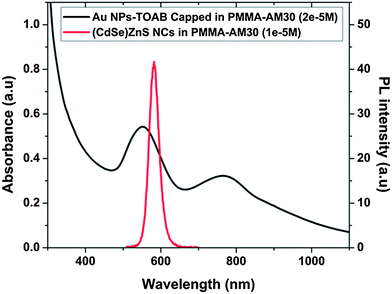 |
| | Fig. 1 Photoluminescence spectrum of the (CdSe)ZnS NCs after their incorporation into the PMMA70-co-MA30 co-polymer at room temperature (excitation wavelength of 420 nm, concentration: 1 × 10⁻⁵ M) (red curve), and absorbance spectrum of Au NPs incorporated into the PMMA70-co-MA30 co-polymer (concentration: 2 × 10⁻⁵ M) (black curve). | |
The absorbance of the synthesized Au NPs incorporated into the PMMA70-co-MA30 co-polymer is presented in Fig. 1 (black curve). The metallic NP polymeric solution exhibits transversal and longitudinal plasmon resonance centered at 551 nm and 768 nm, respectively. The nanoparticles size appeared to be dispersed (details can be found in the ESI†). To apply the numerical model, a unique size of the Au NPs was calculated from the absorbance spectrum of Au NPs incorporated into the PMMA70-co-MA30 co-polymer. Assuming an ellipsoidal shape for the metallic NPs, the average dimension of the metallic NPs was determined numerically using two methods: the Green's-tensor technique25 and the RF COMSOL simulation package. For the calculation, the dielectric constant of Au was taken from Johnson and Chrysty26 The first method provides an accurate electromagnetic description of the system including the local density of states and the local electric field. The long axis of the metallic NPs was found to be 120 nm and the short axis 56 nm. Using these parameters, both methods agree very well when computing the two surface plasmon wavelengths. The distribution of NCs in the co-polymer was determined by TEM. The 'H-bar' method was used, whereby a small slab of the nanocomposite polymer was cut out and mounted on a Cu support ring.27Fig. 2a shows the TEM cross-section image of the spin-coated nanocomposite film showing a homogenous distribution of the (CdSe)ZnS NCs in the polymer matrix.
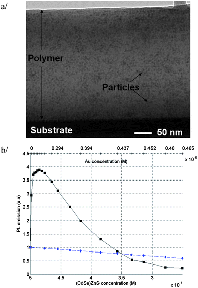 |
| | Fig. 2 (a) TEM cross-section of the PMMA70-co-MA30 co-polymer thin film doped with (CdSe)ZnS NCs. (b) Photoluminescence intensity of the functionalised polymer versus different (CdSe)ZnS NCs and gold Au NP concentrations (curve with solid black squares). The curve with solid blue diamonds presents the PL intensity of (CdSe)Zn diluted in PMMA70-co-MA30 co-polymer for a concentration from 5 × 10⁻⁴ to 2.5 × 10⁻⁴ M without Au NPs. | |
To prepare the polymer mixture with NC emitters and metallic NPs, the pre-synthesized (CdSe)ZnS NCs were diluted in the PMMA70-co-MA30 co-polymer with a concentration of 5 × 10⁻⁴ M. Au NPs were then added in small volume to the polymer–NC doped solution until the concentration of Au NPs in the polymer reached 4.65 × 10⁻⁶ M. Due to the addition of Au NPs in toluene solution, the corresponding NCs concentration in the polymer decreased from 5 × 10⁻⁴ M to 2.5 × 10⁻⁴ M. Each mixture of (CdSe)ZnS NCs and Au NPs was placed in a clean quartz cuvette and its spontaneous emission intensity was measured with a F-2500 fluorescence spectrophotometer under an excitation wavelength of 420 nm and a constant incident intensity. Fig. 2b presents the values of PL intensities, integrated over the whole emission range (500–750 nm), for polymer mixtures containing only (CdSe)ZnS NCs and for polymer mixtures containing (CdSe)ZnS NCs and Au NPs. In the absence of Au NPs, the PL intensity of (CdSe)ZnS NCs decreases linearly. In the presence of Au NPs, an increase of 3.8 times was observed in the (CdSe)ZnS NC PL when the metallic NPs concentration corresponded to 0.2 × 10⁻⁶ M. Further increase in the metallic NPs concentration resulted in a decrease of the PL intensity. For values of Au NP concentration lower than 2 × 10⁻⁶ M, an increasing number of Au NPs allows a coupling between the excitons and localized surface plasmons, therefore the PL intensity increases. At higher concentration of Au NPs, the distance between NPs and NCs decreases which can lead to a quenching of the PL and the increasing number of Au NPs leads to an increasing light absorption. From the concentrations of NCs and NPs, the mean distance among particles was determined assuming a randomly and uniformly distributed noncohesive solution of particles. In the case of hexagonal packing, the mean distance L is approximated by L = 1.1225N0−1/3, where N0 is the density of particles.28,29 The mean distance between Au NPs can be evaluated to be 100 nm and the one between (CdSe)ZnS NCs is about 14 nm.
The modification of the spontaneous emission rate of the exciton–plasmon system was measured using a pulsed diode laser emitting ∼70 ps pulses at 407 nm and with a 10 MHz repetition rate. The PL is then dispersed on a monochromator and detected at the maximum wavelength emission of the (CdSe)ZnS NCs with a photomultiplier. Measurements were performed with a measured bandwidth of 0.64 nm. Fig. 3 shows the emission dynamics of the nanocomposite polymer doped with the optimal concentration of metallic NPs and semiconductor NCs (Fig. 3). In the presence of Au NPs in the polymer, the decay time changes from 9.2 ns to 7.9 ns. The accelerated PL dynamics can be related to the interaction between the NC dipoles and the surface plasmon resonance of the Au NPs. At longer times, above 10 ns, the decay time is similar for all the samples and can be assigned to the recombination of exciton states which are not coupled to the Au NPs. The fast initial decay is consistent with the PL enhancement measured previously (Fig. 2), showing that the PL intensity enhancement is due to a change of the radiative part of the overall decay and that an additional decay channel has to be taken into account.
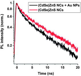 |
| | Fig. 3 Emission dynamics of the nanocomposite polymers with the optimal concentration of Au NPs and of (CdSe)ZnS NCs emitting. Fluorescence lifetime of the nanocomposite polymer with and without Au NPs. | |
To explain our experimental results, a model taking into account the molecular excitation and relaxation near plasmonic systems was used. It combines the Green's tensor technique together with the formalism of the optical Bloch equations. The Green's tensor formalism allows computing the electromagnetic field scattered by a small object embedded in a complex environment, under an arbitrary monochromatic illumination. Starting from the Lippman–Schwinger equation, the total electric field in the whole space can be written as following:30
| |  | (1) |
where
Gnp is the Green's tensor of the environment with the NP,
k20 is the wavevector of the light in the vacuum,
ε is the relative susceptibility of the NP, and
εB is the relative susceptibility of the background. The Green's tensor
Gnp is computed from the Green's tensor
G0 of the environment (without the particle) solving the Dyson equation:
| |  | (2) |
Hence
Gnp(
r,
r′) can be computed numerically for every position (
r,
r′) in the whole space.
31,32 One of the interests of the Green's method is that it allows purely optical properties (Green's function) to be linked to
nanocrystal properties like lifetime, which is strongly modified by the environment. For a two-level system of dipolar moment
d, it is possible to show that the radiative decay rate
Γ(
ω) of a
nanocrystal emitting at
ω is related to the Green's tensor at its location through:
33| | 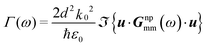 | (3) |
where
u is the unitary vector of the dipole direction.
The band diagram of the (CdSe)ZnS NCs is simplified as a three-level system, as shown on Fig. 4a. In the calculation, the fluorescence process is described as a level |f(ω)〉 emitting at frequency ω. The fluorescence intensity I(ω) emitted at the frequency ω is given by:
| | | I(ω) = ℏωρff(ω)Γ(ω)T(ω) | (4) |
where
| | 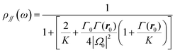 | (5) |
is the population of the fluorescence level |
f(
ω)〉,
Γ(
ω) is the decay rate of the same level,
K and
Γ0 represent respectively the decay rate and the vibrational relaxation decay of state |
e〉. The factor
ρff(
ω) is obtained by solving the optical Bloch equations for the three-levels system in the stationary regime. The decay rate
Γ(
ω) is calculated numerically by computing Green's function
Gnp(
r,
r′) of the environment with the particle.
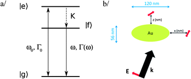 |
| | Fig. 4 (a) Simplified emission band-diagram of the nanocrystal, (b) geometry of the system numerically investigated. The double red arrow represents the NC. | |
Moreover, when the dipole is located in the close vicinity of a metallic object, one part of the emitted light is reabsorbed by the metal. To take into account this effect, the whole expression is multiplied by an extraction factor T(ω), which corresponds to the fraction of the total power Pray emitted by a radiating dipole which is not dissipated inside the gold NP. Hence, Pabs being the power dissipated inside the NP, we have:34
with:
| | | η(ω) = Pabs/Pray = 6πk0∫drε′′(ω)|Gnp(r,r0)·u|2 | (7) |
Eqn (1) is valid for a fixed dipole and a unique incident planewave. However, as both emitters and particles are randomly oriented inside the substrate, the fluorescence light intensity should be averaged on the orientation and polarisation of the incident planewave, and on the dipole orientation. Let us call θ and φ the polar and azimuthal angles, and ψ the angle determining the linear polarization. Similarly, θ′ and φ′ are the corresponding angles for the dipole direction. Then, the averaged fluorescence intensity is written as:
| |  | (8) |
the dependency on
r0 being implicit. As this integral is very long to be numerically evaluated, it was approximated by:
| | 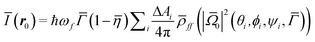 | (9) |
where Δ
Ai is the portion of solid angle around direction (
θi,
ϕi), and:
| |  | (10) |
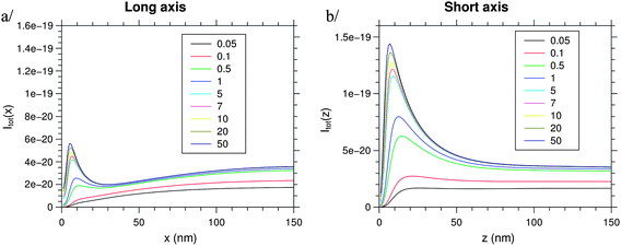
Fig. 5 shows the total averaged intensity Ī emitted by one nanocrystal following the long (Fig. 5a) and short axes (Fig. 5b) of a metallic NPs versus its separation from the edge of the metallic structure. The simulated dependency of the emission intensity of the NC–NP system on the distance between the dipole and the metallic structure is the result of the competition between different energy relaxation mechanisms. For distance d below 5 to 10 nm, the PL is quenched. When the distance is around 10 to 15 nm, the PL is enhanced as shown with recent results.35,36
 |
| | Fig. 5 Total fluorescence intensity for increasing intensity of the excitation light (line colors, the value corresponds to mW, focused on 10 mm2), for a dipole moving along the long (x-) or the short (z-) axis. | |
This calculated optimal distance to couple exciton–plasmon for light emission enhancement is in good agreement with the average interparticle distance calculated experimentally previously. At longer distance d, the dipole does not see anymore the influence of the metallic NPs and the PL intensity saturates. The described behaviour is observed for an intensity density of the excitation light as small as 50 μW mm−2. By separating the different parameters from Ī(ω) such as the population of the fluorescence level, the decay rate, and the extraction factor, one can see that all these parameters participate in the PL enhancement, as shown in Fig. 6 and 7. The decay rate and the local electric field intensity decrease when the distance d decreases, whereas the extraction factor increases. The population of the fluorescence level tends towards zero for short distance d.
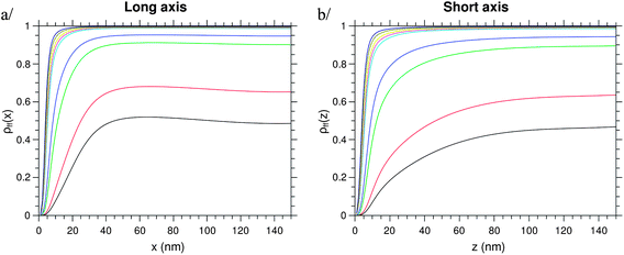 |
| | Fig. 6 Population of the fluorescence state for increasing intensity of the excitation light, for a dipole moving along the long (x-) or the short (z-) axis. Colours correspond to different excitation intensities (see Fig. 5). | |
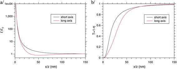 |
| | Fig. 7 Comparison of (a) the decay rate and (b) the extraction factor for a NC moving along the long (x-) or the short (z-) axis. | |
Moreover, striking differences appear between a dipole located near the tip (edge of the long axis) and the side (edge of the short axis) of the NP, as the enhancement factor of the fluorescence light is larger in this latter case. Indeed, there is low enhancement of the extracted light for a dipole near the tip, whereas the enhancement factor can reach much higher values, depending on the incident light intensity, for a dipole near the side. If no obvious differences between the two appear on the population of the fluorescence level, both the decay rate and the extraction factors change favourably when the dipole moves from the tip to the side of the NP, as can be seen in Fig. 7. These differences can be attributed to the fact that the emission wavelength is closer to the first plasmon resonance at 551 nm than the second at 768 nm: the decay rate is then larger near the side than near the tip of the NP.
The variation in the extraction factor is more difficult to understand, as the absorption is supposed to increase near the resonance. However due to the large size of the particle, it is reasonable to suppose that the amount of energy scattered by the particle increases faster than the dissipation when the wavelength goes closer to the plasmon wavelength, as the absorption cross-section of small NPs is much larger than their scattering cross-section. In the case of NPs, the extraction factor increases when the dipole moves to the side of the particle as shown in Fig. 7. From these simulations, it is clear that the shape of the metallic NPs taken into account by the extraction factor can play a key role in the diffraction of the light in the far-field. This subject is under further investigation.
The nanocomposite polymer composed of semiconducting NCs and the Au NP solution at their optimal concentration was spin-coated on a quartz substrate with a polymer thickness of the 300 nm. However, under these conditions, the majority of the emitted light was mainly trapped in the polymer film. A solution consists of using two-dimensional (2D) photonic crystals (PhCs)37 to transfer patterns of photonic crystal structures into polymer films to extract light out of the plane. We used nanoimprint lithography (NIL) which is a suitable and efficient technique with high resolution (down to sub-10 nm) and excellent fidelity onto a very large number of organic compounds.38 Silicon stamps were fabricated using conventional lithographic techniques (details can be found in the ESI†).
The nanocomposite polymer was printed with the PhCs stamp by standard thermal NIL using a 2.5 inch Obducat nanoimprinting machine. The nanocomposite was printed at 170 °C at a pressure of 60 bars for 500 s Fig. 8a presents a SEM picture showing the excellent pattern transfer of the stamp nanostructures to the nanocomposite polymer. A TEM cross-section of the imprinted co-polymer with (CdSe)ZNs NCs was performed as shown in Fig. 8b. Au NPs could not be incorporated at the time to perform a TEM cross-section study. A continuous wave Ar+ laser at a wavelength of 514.5 nm, with a power of 50 μW focused down to a 20 μm spot with the incident beam normal to the surface was used, through a ×10 microscope objective with a numerical aperture NA = 0.4, to pump the nanocomposite polymer. PL spectra from the collection spot were measured normally to the surface and analyzed with an optical spectrum analyzer. The nanoimprint process has a negligible impact on the PL properties of the NCs as no difference was found measuring the PL before and after the nanoimprinting process. Fig. 9 shows PL spectra of a nanoimprinted unpatterned sample without Au NPs (black curve), of a nanoimprinted unpatterned sample with the optimal concentration of Au NPs and NCs (red curve, PL enhancement by a factor 3.8) and of a 500 nm honeycomb lattice photonic crystal with the optimal concentration of Au NPs and NCs (green curve). It is observed that the PL intensity for the PhC is 7.9 (green curve) as large as that of the PL intensity of the unpatterned substrate without the Au NPs (black curve). The NCs emission linewidth falls above the light cone in a high density of state area (2D band diagram not shown). This results in very low-group-velocity photons and an enhanced coupling to the radiative modes out of plane.
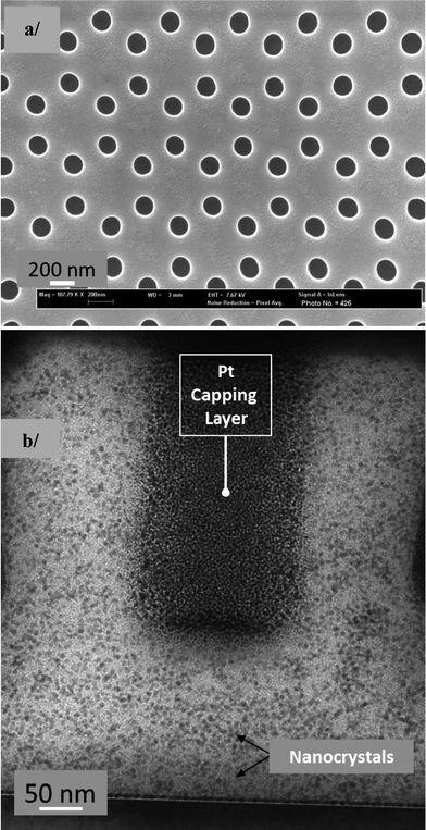 |
| | Fig. 8 (a) SEM micrograph of the nanoimprinted photonic crystal (top-view), (b) TEM cross-section of the nanoimprinted photonic crystals showing the homogenous NC dispersion in the nanoimprinted nanocomposite polymer (no Au NPs were incorporated). | |
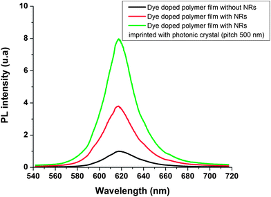 |
| | Fig. 9 PL spectra of the (CdSe)ZnS NC doped polymer film with and without Au NPs (red and black curves respectively), PL spectra of dye doped polymer film with Au NPs imprinted with 2D photonic crystal (pitch 500 nm, green curve). | |
In conclusion, we observed a coupling between semiconductors NCs and metallic NPs in a printable polymer which leads to an enhancement of the spontaneous emission rate of the NCs. The Green's tensor method is combined with the optical Bloch formalism to study the modification of the fluorescence of an emitter placed in the vicinity of a metallic particle. We demonstrate that the nanocomposite polymer can be patterned by NIL to fabricate efficient light extractors as photonic crystals. Our results indicate that nanoimprint lithography is well suited to fabricate these challenging photonic structures and that the combination of surface plasmons and nanoimprinted photonic structures in an active layer may lead to a new class of cost effective and high efficient components.
Acknowledgements
This work was supported by the EC project NaPaNIL (Contract no. 214249), the MICINN project ACPHIN (contract no. FIS2009-150) and the Catalan project 2009-SGR-150. The content of this work is the sole responsibility of the authors.
References
- J. Zhang, Y. Fu, M. H. Chowdhury and J. R. Lakowicz, Nano Lett., 2007, 7, 2101–2107 CrossRef CAS.
- A. Bek, R. Jansen, M. Ringler, S. Mayilo, T. A. Klar and J. Feldmann, Nano Lett., 2008, 8, 485–490 CrossRef CAS.
- P. Anger, P. Bharadwaj and L. Novotny, Phys. Rev. Lett., 2006, 96, 113002 CrossRef.
- E. Dulkeith, A. C. Morteani, T. Niedereichholz, T. A. Klar, J. Feldmann, S. A. Levi, F. C. J. M. van Veggel, D. N. Reinhoudt, M. Moller and D. I. Gittins, Phys. Rev. Lett., 2002, 89, 203002 CrossRef CAS.
- G. Schneider, G. Decher, N. Nerambourg, R. Praho, M. H. V. Werts and M. Blanchard-Desce, Nano Lett., 2006, 6, 530–536 CrossRef CAS.
- G. L. Liu, Y.-T. Long, Y. Choi, T. Kang and L. P. Lee, Nat. Methods, 2007, 4, 1015–1017 CrossRef CAS.
- A. Wokaun, H. P. Lutz, A. P. King, U. P. Wild and R. R. Ernst, J. Chem. Phys., 1983, 79, 509 CrossRef CAS.
- N. T. Fofang, T.-H. Park, O. Neumann, N. A. Mirin, P. Nordlander and N. J. Halas, Nano Lett., 2008, 8, 3481–3487 CrossRef CAS.
- J.-Y. Yan, W. Zhang, S. Q. Duan, X.-G. Zhao and A. O. Govorov, Phys. Rev. B: Condens. Matter Mater. Phys., 2008, 77, 165301 CrossRef.
- A. Ueda, T. Tayagaki and Y. Kanemitsu, Appl. Phys. Lett., 2008, 92, 133118 CrossRef.
- S. Y. Lee, K. Nakaya, T. Hayashi and M. Hara, Phys. Chem. Chem. Phys., 2009, 11, 4403–4409 RSC.
- Y. Fedutik, V. V. Temnov, O. Schops, U. Woggon and M. V. Artemyev, Phys. Rev. Lett., 2007, 99, 136802 CrossRef CAS.
- A. V. Akimov, A. Mukherjee, C. L. Yu, D. E. Chang, A. S. Zibrov, P. R. Hemmer, H. Park and M. D. Lukin, Nature, 2007, 450, 402–406 CrossRef CAS.
- H. Wei, D. Ratchford, X. Li, H. Xu and C.-K. Shih, Nano Lett., 2009, 9, 4168–4171 CrossRef CAS.
- Y. Chen, K. Munechika, I. J.-L. Plante, A. M. Munro, S. E. Skrabalak, Y. Xia and D. S. Ginger, Appl. Phys. Lett., 2008, 93, 053106 CrossRef.
- J.-H. Song, T. Atay, S. Shi, H. Urabe and A. Nurmikko, Nano Lett., 2005, 5, 1557–1561 CrossRef CAS.
- P. P. Pompa, L. Martiradonna, A. D. Torre, F. D. Sala, L. Manna, M. D. Vittorio, F. Calabi, R. Cingolani and R. Rinaldi, Nat. Nanotechnol., 2006, 1, 126–130 CrossRef CAS.
- P. Hobson, S. Wedge, J. Wasey, I. Sage and W. Barnes, Adv. Mater., 2002, 14, 1393–1396 CrossRef CAS.
- J. Vuckovic, M. Loncar and A. Scherer, IEEE J. Quantum Electron., 2000, 36(10), 1131–1144 CrossRef CAS.
- D. E. Gomez, K. C. Vernon, P. Mulvaney and T. J. Davis, Nano Lett., 2010, 10, 274–278 CrossRef CAS.
- Jana,
et al.
, Small, 2005, 1, 875 CrossRef CAS.
- C. Sönnischsen, T. Franzl, T. Wilk, G. von Plessen and J. Feldmann, J. Phys. Rev. Lett., 2002, 88, 077402 CrossRef.
- L. Qu and X. Peng, J. Am. Chem. Soc., 2002, 124, 2049–2055 CrossRef CAS.
- M. Tamborra, M. Striccoli, M. L. Curri, J. A. Alducin, D. Mecerreyes, J. A. Pomposo, N. Kehagias, V. Reboud, C. M. Sotomayor Torres and A. Agostian, Small, 2007, 3(5), 822 CrossRef CAS.
- O. J. F. Martin, C. Girard and A. Dereux, Phys. Rev. Lett., 1995, 74, 526 CrossRef CAS.
- P. B. Johnson and R. W. Chrysty, Phys. Rev. B: Solid State, 1972, 6, 4370–4379 CrossRef CAS.
- S. B. Newcomb, Inst. Phys. Conf. Ser., 2004, 179, 357–362 CAS.
- Y. N. Kryuchkov, Refract. Ind. Ceram., 2001, 42, 390–392 CrossRef.
- E. J. Meijer and D. Frenkel, J. Chem. Phys., 1994, 100, 6873 CrossRef CAS.
- G. Colas des France, C. Girard, T. Laroche, G. Lévêque and O. J. F. Martin, J. Chem. Phys., 2007, 127, 034701 CrossRef.
- O. J. F. Martin and N. B. Piller, Phys. Rev. E: Stat. Phys., Plasmas, Fluids, Relat. Interdiscip. Top., 1998, 58, 3909 CrossRef CAS.
- M. Paulus and O. J. F. Martin, J. Opt. Soc. Am. A, 2001, 18, 854 CrossRef.
- C. Girard, O. J. F. Martin, G. Leveque, G. Colas des Francs and A. Dereux, Chem. Phys. Lett., 2005, 404, 44 CrossRef CAS.
- G. Baffou, C. Girard, E. Dujardin, G. Colas des Francs and O. J. F. Martin, Phys. Rev. B: Condens. Matter Mater. Phys., 2008, 77, 121101 CrossRef (R).
- P. Anger, P. Bharadwaj and L. Novotny, Phys. Rev. Lett., 2006, 96, 113002 CrossRef.
- O. Kulakovich,
et al.
, Nano Lett., 2002, 2, 1449 CrossRef CAS.
- Y. R. Do, Y.-C. Kim, Y.-W. Song, C.-O. Cho, H. Jeon, Y.-J. Lee and S.-H. Kim, Adv. Mater., 2003, 15, 1214 CrossRef CAS.
- S. Y. Chou, P. R. Krauss and P. J. Renstrom, Science, 1996, 272, 85 CAS.
Footnote |
| † Electronic supplementary information (ESI) available. See DOI: 10.1039/c2nr32134c |
|
| This journal is © The Royal Society of Chemistry 2013 |
Click here to see how this site uses Cookies. View our privacy policy here.