DOI:
10.1039/C3NJ00815K
(Paper)
New J. Chem., 2014,
38, 70-76
One-pot solvothermal synthesis and properties of 1D NiSe and NiSe–Ni3S2 alloyed compound nanorod arrays†
Received
(in Montpellier, France)
23rd July 2013
, Accepted 30th September 2013
First published on 2nd October 2013
Abstract
A general one-pot solvothermal route was adopted to produce well-aligned NiSe and NiSe–Ni3S2 compound nanorod arrays on an Ni substrate. Metal foil was used as nickel source, and it also favored the unidirectional diffusion of metal ions, resulting in the vertical growth of one dimensional nanostructures on the substrate. Elemental mapping showed that the NiSe–Ni3S2 composite was an alloyed nanoheterostructure, which had paramagnetic behavior. Luminescence properties at room temperature indicated that the ultraviolet luminous intensity of the alloy materials could be significantly enhanced through doping Ni3S2 into the NiSe sample.
1. Introduction
During the past few decades, well-aligned semiconductor nanowire and nanorod arrays have attracted considerable attention owing to their potential applications in novel optoelectronic nanodevices, such as light-emitting diodes, field emission transistors, laser diodes, and sensors.1–6 Nickel selenide, a member of the transition metal chalcogenides with Pauli paramagnetism and metallic conductivity, has been regarded as a typical material for studying the physical characteristics of electron systems with narrow bands.7 In addition, nickel selenides have been found applications in the fields of catalyst, optical recording, solar cells, lithium ion cells, laser materials and energy storage.8–11 Because of the valence electronic configuration of Ni (3d84s2) and the small difference in electronegativity between Ni (χ = 1.9) and Se (χ = 2.4), nickel and selenium can form a variety of complexes with varied stoichiometries.12 Many methods have been developed for the synthesis of nickel selenides, such as ultrasonic synthesis, elemental reactions, mechanical alloying and mixed-solution synthesis.13,14 A variety of well-defined shapes such as nano/microspheres, flower-like architectures, nanowires, six-horn nanostars, hollow spheres, tubes and octahedra have thus been obtained.15–19 There have been several prior research works on nickel sulfides and Ni(OH)2 nanostructures that were formed on nickel foil.20–22 Even so, there are few reports on the growth of nanorod arrays directly on a nickel substrate via a solvothermal method.
1D multiple-component nanostructures, such as alloyed nanowires and nanorods may offer unique properties compared to their counterparts.23 Furthermore, adjusting the stoichiometry of the constituent components can effectively tune their properties. Several kinds of synthetic strategies have been attempted to fabricate such 1D alloyed compounds, including template assisted electrodeposition processes, sol–gel spin coating methods, and chemical vapor deposition methods.24–26
Nickel sulfide and nickel selenide are p-type semiconductors with band gaps of 0.3 eV and 2.0 eV, respectively, exhibiting interesting electronic and magnetic properties.27,28 Upon introducing dopants, they present new properties. For example, Schuster's group discussed the electronic and magnetic properties of Se-doped and compressed NiS2 in detail, and they found the microscopic origin of the metal–insulator and antiferromagnetic–paramagnetic transitions in NiS2–xSex.29 The NiS2–xSex properties can be altered by varying the composition of the anion sublattice.30 On the other hand, well-aligned nanowire and nanorod arrays on substrates are highly attractive for device applications. For instance, Ni3S2 nanowire arrays present higher discharge–charge capacities and reversible lithium capacities than Ni3S2 thin film in lithium-ion battery electrode applications.31 Additionally, various nickel sulfides have been obtained by a solvothermal process.20,32 However, developing a simple method to synthesize 1D NiSe–Ni3S2 alloyed compound nanorod arrays on substrates with regular morphology and controlled composition remains a challenge.
Herein, we used solvothermal routes to produce uniform 1D NiSe and NiSe–Ni3S2 compound nanorod arrays directly on a nickel substrate in one step. The nickel substrate was used as the support and nickel source in the process. The method is simple, convenient and effective to obtain metal chalcogenide array materials. As far as we know, there are few reports on the preparation of NiSe–Ni3S2 alloyed compound nanorod arrays so far.
2. Experimental
2.1 Materials
Nickel foil (Aldrich, purity: 99.5%, thickness: 0.15 mm), selenium powder (Se, ≥99.5%), sulfur powder (S, ≥99.5%) and hexadecyl trimethyl ammonium bromide (CTAB) were purchased from Shanghai Chemical Reagent. Anhydrous alcohol and hydrazine hydrate (N2H4·H2O, 80 wt%) were of analytical grade, All chemicals and solvents were used directly without any further purification. Distilled water was used in all the experiments.
2.2 Treatment of the nickel foil
A piece of nickel foil (2.0 cm × 1.0 cm) was treated with nitric acid aqueous solution and ultrasonically cleaned for 5 min. After that, the Ni substrate was rinsed with anhydrous alcohol for 5 min. Then the substrate was dried under ambient air conditions.
2.3 Synthesis of NiSe and NiSe–Ni3S2 nanorod arrays
0.1776 g of selenium powder was dissolved in 15 ml of hydrazine hydrate with vigorous magnetic stirring. Subsequently, a certain amount of surfactant (CTAB) was added into the above solution and the mixture was stirred at room temperature until its color changed to brownish black. After that, the reactants were transferred into a 50 ml Teflon-lined autoclave with a piece of cleaned Ni foil immersed. The autoclave was sealed and maintained at 140 °C for 12 h and then air-cooled to room temperature naturally. The Ni foil was taken out of solution, rinsed repeatedly with ethanol, and finally dried in air for further characterization. Similarly, NiSe–Ni3S2 nanoheterostructures were constructed in the same way as for the NiSe except that sulfur powder was added into the hydrazine hydrate after the selenium powder. As a control experiment, we synthesized Ni3S2 nanorod arrays by keeping the molar ratio of S and Se as 1![[thin space (1/6-em)]](https://www.rsc.org/images/entities/char_2009.gif) :1.
:1.
2.4 Characterization
X-Ray diffraction (XRD) spectra of the products were measured on a Phillips X’Pert materials research diffractometer using secondary graphite monochromatized Cu Kα radiation (λ = 1.54 Å). X-ray photoelectron spectroscopy (XPS) was performed on an FSLP920 X-ray photoelectron spectrometer using a non-monochromatized Mg Kα X-ray as the excitation source. The examination of the morphology was carried out with a scanning electron microscope using a Philips XL-30ESEM equipped with an energy dispersive X-ray spectroscope (EDS) operating at 10 kV accelerating voltage. The nickel selenide nanorod arrays were scraped from the nickel substrate mechanically, and dispersed in an alcohol solution ultrasonically, then deposited on carbon-coated copper grids for transmission electron microscope (TEM) characterization. A JEOL-2010 high-resolution transmission electron microscope (HRTEM) operating at 200 kV was used to examine the nanostructures. An EDS attached to the TEM was utilized to determine the chemical composition of the nanostructures. Power-dependent photoluminescence (PL) at room temperature was studied on an FSLP920 fluorescence spectrophotometer. The magnetic measurements of the nanorod arrays were carried out with a superconducting quantum interference device (SQUID) magnetometer (MPMS-5) within the temperature range of 2–300 K. The temperature-dependent magnetization curves and the magnetization versus applied magnetic field curves at 2 K were measured with zero-field-cooling (ZFC) and field-cooling (FC) processes at an applied field of 1000 Oe in powder state.
3. Results and discussion
3.1 SEM analysis
Uniform 1D NiSe and NiSe–Ni3S2 compound nanorod arrays were synthesized directly on the nickel substrate by a one-pot solvothermal reaction. The top-view and tilted SEM images of the NiSe product are shown in Fig. 1, and they demonstrate the growth of vertically aligned large-area NiSe nanorods with uniform diameter distributions. The shapes and sizes of the nickel selenide nanostructures could be controlled by tuning the amount of CTAB. Without CTAB (Fig. 1a and b), the top parts of the nanorods are slightly bent, and the diameters of the nanorods are about 40–80 nm. With the addition of 0.3 mmol CTAB, the nanorod arrays exhibit lengths of ca. 2–3 μm and diameters of 80–140 nm (Fig. 1c and d). Each nanorod has a smooth surface and a needle-like tip. However, the nanorod arrays are partially agglomerated in bundles (Fig. 1d). When 0.75 mmol CTAB is used, regular columnar nanorods are obtained on the nickel foil surface. The lengths of the nanorods are about 2 μm, and the diameters are about 90–180 nm. They are parallel to each other and vertical to the nickel foil with a strong preference for a specific direction (Fig. 1e and f). This illustrates the role of CTAB in promoting the orderly growth. The NiSe sample shown in Fig. 1e and f is used as a representative sample in the following research.
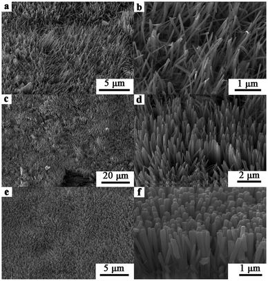 |
| | Fig. 1 SEM images of the NiSe products obtained with (a, b) 0 mmol CTAB; (c, d) 0.3 mmol CTAB and (e, f) 0.75 mmol CTAB by solvothermal reaction at 140 °C for 12 h. | |
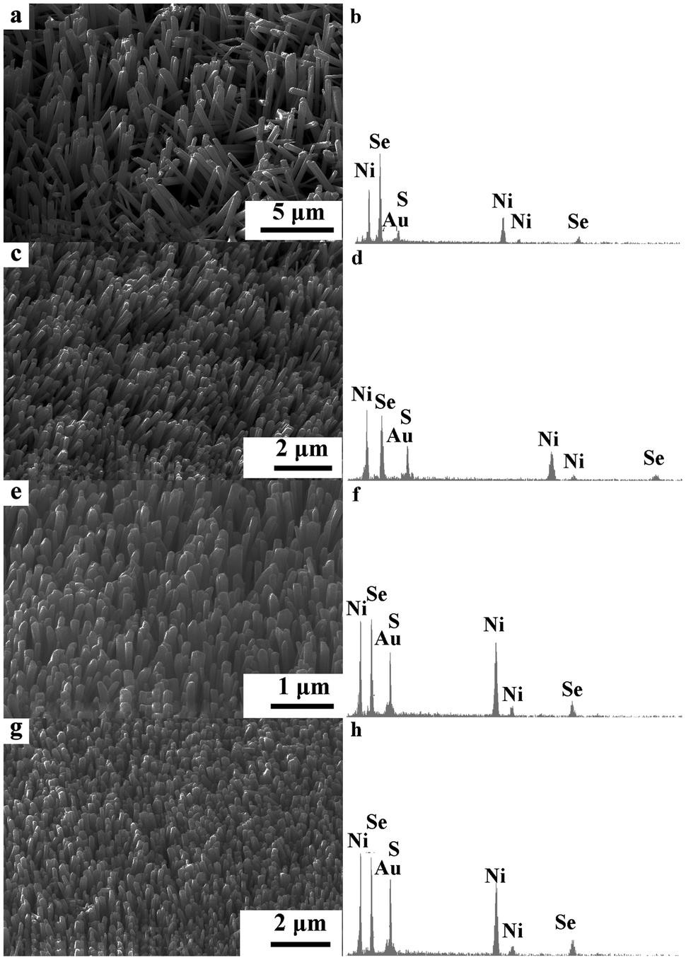
The SEM images of the NiSe–Ni3S2 composites with different S/Se raw material ratios are shown in Fig. 2. They all appear as nanorod arrays with little difference compared to the NiSe. In addition, EDS spectra of the as-synthesized products were recorded to characterize the chemical compositions of these nanorods, as shown in Fig. 2b, d, f and h. The detectable elements in these composites include Ni, S and Se. Moreover, it was found that with the increase of the original reactant ratio (S/Se), the molar ratio of the S/Se is also increased in the EDS spectra. In the following research, the NiSe–Ni3S2 composite in Fig. 2e is selected as a representative sample.
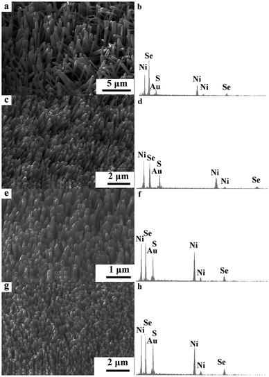 |
| | Fig. 2 SEM images of the as-prepared NiSe–Ni3S2 composite with different molar ratios of sulfur and selenium (S/Se): (a) 1:1, (c) 3:1, (e) 5:1, (g) 10:1. The right side (b, d, f, h) shows the corresponding EDS spectra of the left products (a, c, e, g). | |
3.2 XRD analysis
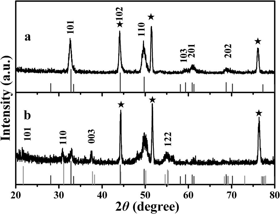
Fig. 3a depicts the XRD pattern of the NiSe film product. The diffraction peaks marked with ★ that show high intensities correspond to the metallic nickel substrate. All the diffraction peaks can be assigned to the NiSe and Ni substrate, and no diffraction peaks of any other impurities are observed. These peaks are in good agreement with the literature values for NiSe (JCPDS card no. 65-9451), and the obtained NiSe is a hexagonal structure (space group P63/mmc, no. 194). The cell parameters of the products are a = 3.658 Å and c = 5.354 Å. Additionally, the diffraction intensity for the (110) plane is a bit stronger than that of the JCPDS standard file, suggesting a preferential orientation growth of the NiSe crystal along the c axis.33–36 The XRD pattern of the NiSe–Ni3S2 composite (Fig. 3b) can be indexed as NiSe, Ni3S2 (JCPDS card 44-1418) and the nickel substrate. Aside from the peaks of the NiSe and nickel substrate, the other peaks can be assigned to the heazlewoodite Ni3S2 corresponding to the (101), (110), (003) and (122) planes and the fractional NiSe peaks disappear or become weakened.
 |
| | Fig. 3 The XRD patterns of the NiSe (a) and NiSe–Ni3S2 (b) products (S/Se = 5:1). The stars (★) show the characteristic peaks of the Ni substrate. | |
3.3 XPS analysis
XPS spectra were employed to further evaluate the quality and surface composition of the as-synthesized products. In Fig. 4a, the characteristic peaks of Ni and Se are observable in the XPS survey spectrum of the NiSe. Fig. 4b exhibits the XPS spectrum of the NiSe–Ni3S2 compound, and the peaks of Ni, Se and S are detected. Fig. 4c to e show the XPS spectra of the Ni 2p, Se 3d, and S 2p region in Fig. 4b. As shown in Fig. 4c, the Ni 2p 3/2 and Ni 2p 1/2 peaks appear at 856.1 eV and 874.1 eV, respectively. The two peaks are a good match with NiSe and Ni3S2,37,38 whereas the other two peaks located at 852.8 eV and 870.4 eV can be attributed to metallic Ni 2p,37 which comes from the nickel substrate. The strong peak at around 54.3 eV (Fig. 4d) belongs to Se 3d,39 and the peak located at 160.7 eV (Fig. 4e) can be assigned to S 2p. There is a broad peak with a surface binding energy of 158.9–162.9 eV, and the peak can be fitted with two spin-orbit-split doublets corresponding to Se 3p at 160.8 eV and S 2p at 161.8 eV. In these two regions, the Se 3p and S 2p are partially overlapped. The signal at 283.6 eV (Fig. 4a and b) is attributed to the binding energy of C 1s. Additionally, the peak at 531.1 eV can be attributed to O 1s, and it is derived from the unavoidable oxygen adsorption on the surfaces of the products.
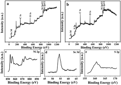 |
| | Fig. 4 (a and b) XPS spectra of the NiSe and NiSe–Ni3S2 nanorod array products (S/Se = 5:1). (c–e) XPS spectra of the Ni 2p, Se 3d and S 2p region in NiSe–Ni3S2. | |
3.4 TEM analysis
A typical TEM image shows that the NiSe consists of 1D nanorods (Fig. 5a). HRTEM images were used to detect the fine structure of the NiSe nanorods, as shown in Fig. 5b. The inset shows the corresponding fast Fourier transform (FFT) diffraction. Both the regularity of the lattice plane in the HRTEM image and the FFT image reveal the NiSe nanorod is a single crystal. The lattice fringes between adjacent planes with a d-spacing of 0.182 nm in the HRTEM image (Fig. 5c) correspond to the (110) plane of the NiSe.
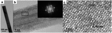 |
| | Fig. 5 (a) TEM image of a typical NiSe nanorod sample, (b) HRTEM image of NiSe nanorod structure, the inset shows the corresponding FFT image, (c) the magnified image of (b). | |
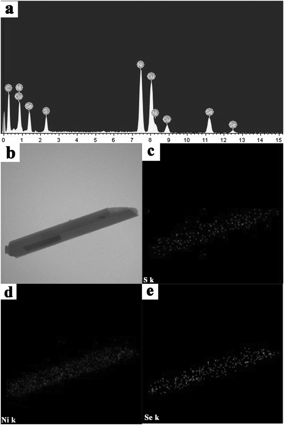
To further confirm the composition of the as-prepared NiSe–Ni3S2 nanocrystalline composite material, an EDS spectrum (Fig. 6a) using an instrument attached to the TEM was recorded for an individual nanorod, and it indicates the presence of Ni, S and Se. In addition, the peaks of C and Cu originate from the copper grid. However, the EDS spectrum analysis cannot provide overall information about how these elements are distributed and the spatial variation in the chemical composition. To distinguish the distribution of the Ni, S and Se elements in the rod-like products, elemental mapping of a single nanorod (Fig. 6b) removed from the nickel substrate was performed. The results (Fig. 6c to e) reveal that S, Ni and Se atoms are well-dispersed within the entire nanorod. They exhibit random element intermixing that rules out the formation of core–shell structures or NiSe and Ni3S2 phase segregation as major components. In addition, the elemental mapping suggests the Ni content is more than that of the other two because the products were obtained from the Ni substrate. On the other hand, the NiSe–Ni3S2 compound was synthesized by using the original molar ratio of 5:1 for S/Se, but the amount of selenium is greater than that of sulfur (Fig. 6c and e). This is because nickel selenide is easier to form than nickel sulfide depending on the thermodynamic feasibility that is estimated from ΔG0298 under the same conditions.40 On the basis of the above results, we can conclude that the as-prepared NiSe–Ni3S2 nanorod compound is definitely an alloyed material.
 |
| | Fig. 6 NiSe–Ni3S2 compound (S/Se = 5:1): (a) EDS pattern, (b) TEM image of the nanorod, (c–e) S, Ni and Se elemental mapping of the nanorod. | |
3.5 The possible growth mechanism for the 1D alloyed compound nanostructure
In order to investigate the growth mechanism of the alloyed compound, we performed several time-dependent experiments under conditions that were otherwise the same. Nearly no products were observed on the surface of the substrate before 1 h and the XRD, SEM and EDS measurements of the samples at different reaction times (1 h, 2 h, 4 h and 8 h) can be found in the ESI.† According to the XRD patterns (shown in the ESI,† Fig. S1), we can see that the NiSe and Ni3S2 exist at different reaction times. From the SEM images (shown in the ESI,† Fig. S2a, c, e and g), a tendency to form the nanorods occurred at 1 h. Upon increasing the reaction time, the lengths of the nanorods gradually became longer, and finally the nanorod arrays formed. The EDS spectra (shown in the ESI,† Fig. S2b, d, f and h) confirm that all the nanorod arrays were composed of Ni, S and Se at different deposition times. Because the composite was synthesized using the original molar ratio of 5:1 for S/Se, S-rich alloyed NiSe–Ni3S2 nanorod arrays were obtained in the initial stage, although nickel selenide is easier to form than nickel sulfide. On the other hand, the molar ratio of Se/S is gradually increased with the increase of the reaction time. It is most probable that the smaller sulfide ions were replaced by the larger selenide ions. This is similar to the reported literature.40 Based on the experimental results described above, we consider that the formation of the NiSe and Ni3S2 phase is the result of a combination of codepositions. They are deposited on the nickel substrate at almost the same time, thus forming the alloyed NiSe–Ni3S2 nanorod arrays.
3.6 Magnetic property studies
The temperature dependence of the magnetization of the Ni3S2, NiSe and NiSe–Ni3S2 composite material are shown in Fig. 7a to c. This was recorded upon heating the sample in a field of 1000 Oe using ZFC and FC modes. At 2–30 K, the FC magnetization rapidly increases with decreasing temperature. This behavior could be attributed to the surface spins, which are frozen in the external field direction.41 At higher temperatures, the particle moments are free to undergo thermal fluctuations and the FC and ZFC curves merge together. For the Ni3S2 and NiSe nanorod arrays samples (Fig. 7a and b), in the low temperature region, one striking feature is that a peak is observed in the ZFC curves, at the blocking temperature, TB. This is ascribed to the freezing behavior of these samples, and this behavior is mainly due to the strong interparticle dipolar magnetic interactions.42,43 There is a bifurcation between the FC and ZFC curves at TB, and the divergence point is defined as the irreversible temperature (Tirr). Below this temperature, the two curves diverge, which implies a magnetically frustrated system which should be described as a spin-glass.44 The FC curve shows a uniform decay and reaches the ZFC curve close to the peak, suggesting superparamagnetic (SPM) behavior at high temperature.41 Both TB and Tirr almost completely overlap, indicating a narrow size distribution of the SPM particles.45 In Fig. 7a and b, the TB of the Ni3S2 is about 7.9 K, whereas the TB value for the NiSe is about 4.9 K (Fig. 7d). However, in the case of the alloyed nanoheterostructure, a peak in the ZFC curve (Fig. 7c) was not found. This could be attributed to the presence of a paramagnetic phase, which has very low unblocking temperatures.44,46 The maximum magnetization of the Ni3S2 is higher than that for the NiSe, so the magnetization intensity of the alloyed nanoheterostructure is drastically enhanced by doping Ni3S2 into the NiSe. However it still lies between the two components. This is also in agreement with the findings of the following hysteresis curve analysis.
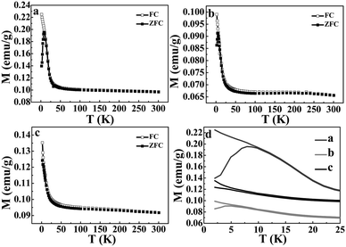 |
| | Fig. 7 FC and ZFC measurements for different nanorod samples with applied fields of 1000 Oe: (a) Ni3S2, (b) NiSe, (c) NiSe–Ni3S2 heterostructure (S/Se = 5:1), (d) FC and ZFC curves of (a), (b) and (c) in the range 2–25 K. | |
The magnetization versus applied magnetic field curves for the three samples were measured at 2 K. As shown in Fig. 8, all the magnetizations of the Ni3S2, NiSe and NiSe–Ni3S2 present a characteristic loop of ferromagnetic behavior with a coercive field (HC) of 740 Oe, 213 Oe and 213 Oe, respectively. The difference in coercivity can be attributed to different surface anisotropy that seems to control the HC value.47,48 There is also remnant magnetization at 2 K of 0.124 emu g−1, 0.019 emu g−1 and 0.028 emu g−1 for the Ni3S2, NiSe and NiSe–Ni3S2, respectively, further revealing a weak ferromagnetism at low temperature.
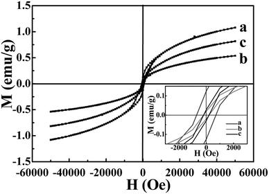 |
| | Fig. 8 Hysteresis loops measured at 2 K for (a) Ni3S2, (b) NiSe, and (c) NiSe–Ni3S2 composite material (S/Se = 5:1), the inset shows the magnified image. | |
3.7 PL property studies
The optical properties of the products at room temperature were characterized by PL spectra (Fig. 9) in the powder state. All of the products show emission spectra with PL excitation at 248 nm. The PL spectrum of the NiSe has a weak and broad peak at 374 nm. The optical properties of the NiSe are mainly controlled by the intrinsic defects, and excess Se ions or Ni ions may induce various structural defects, such as Ni vacancies or Se vacancies.49,50 The PL emission spectra of the Ni3S2 and NiSe–Ni3S2 alloyed compounds both show a strong peak at 392 nm. A red shift occurs in the peak position of the NiSe–Ni3S2 compared to the undoped NiSe crystals. The effects of the Ni3S2 dopant on the luminous intensity of the NiSe have been determined. The intensity of the PL peak of the nanoheterostructure gradually increases as the amount of the dopant increases. Because the selenium atom has a larger radius than the sulfur atom, it facilitates the formation of defects in the alloyed compound, thus affecting the optical characteristics of the entire system. Doping NiSe nanocrystals with Ni3S2 is therefore expected to be a straightforward process for the generation of nanocrystals with tunable optical properties, and it is promising for use in solution-processable devices.
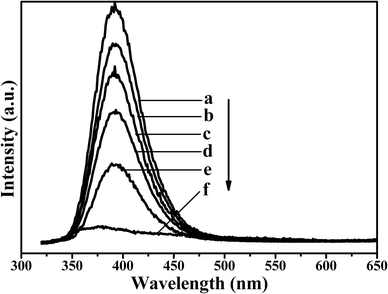 |
| | Fig. 9 Room temperature PL spectra of the as-prepared (a) Ni3S2, (f) NiSe and NiSe–Ni3S2 alloyed compound obtained with the original molar ratio of S/Se of (b) 10:1, (c) 5:1, (d) 3:1, (e) 1:1. | |
4. Conclusions
We have demonstrated a facile one-pot solvothermal synthesis of uniform NiSe and NiSe–Ni3S2 nanorod arrays that were grown directly on Ni substrates. By comprehensive characterization using XRD analysis, EDS mapping, and XPS analysis, it was proved that the NiSe–Ni3S2 composition is that of an alloyed nanoheterostructure. Magnetic characterization suggested that the behavior of the obtained NiSe–Ni3S2 nanoheterostructures transformed into paramagnetism, and the magnetization intensity of the NiSe–Ni3S2 sample lay between that of the two components. The optical properties of the alloyed nanoheterostructure arrays indicated that the higher Ni3S2 doping levels led to a higher photoluminescence intensity through adjusting the S/Se raw material ratio.
Acknowledgements
This work was supported by the Natural Science Fund of China (no. 21073031, 20573017).
Notes and references
- M. H. Huang, S. Mao, H. Feick, H. Q. Yan, Y. Y. Wu, H. Kind, E. Webber, R. Russo and P. D. Yang, Science, 2001, 292, 1897–1899 CrossRef CAS PubMed
 .
.
- P. Nguyen, H. T. Ng, T. Yamada, M. K. Smith, J. Li, J. Han and M. Meyyappan, Nano Lett., 2004, 4, 651–657 CrossRef CAS .
- Y. Liu, A. Liu, W. Liu, Z. Hu and Y. Sang, Appl. Surf. Sci., 2010, 257, 1263–1266 CrossRef CAS PubMed .
- X. Zhou, W. Fu, H. Yang, Y. Mu, J. Ma, L. Tian, B. Zhao and M. Li, Mater. Lett., 2013, 93, 95–98 CrossRef CAS PubMed .
- F. Zheng, M. Zhang and M. Guo, Thin Solid Films, 2013, 534, 45–53 CrossRef CAS PubMed .
- K. Q. Peng, Z. P. Huang and J. Zhu, Adv. Mater., 2004, 16, 73–76 CrossRef CAS .
- A. Y. Matsuura, H. Watamable, C. Kim, S. Doniach, Z. X. Shen, T. Thio and J. W. Bennett, Phys. Rev. B: Condens. Matter Mater. Phys., 1998, 58, 3690–3696 CrossRef CAS .
- X. Wang, J. Zhuang, Q. Peng and Y. D. Li, Nature, 2005, 437, 121–124 CrossRef CAS PubMed .
- B. Liu, J. Zhang, X. F. Wang, G. Chen, D. Chen, C. W. Zhou and G. Z. Shen, Nano Lett., 2012, 12, 3005–3011 CrossRef CAS PubMed .
- B. X. Yuan, W. L. Luan and S. T. Tu, CrystEngComm, 2012, 14, 2145–2151 RSC .
- L. Mi, Q. Ding, H. Sun, W. Chen, Y. Zhang, C. Liu, H. Hou, Z. Zheng and C. Shen, CrystEngComm, 2013, 15, 2624–2630 RSC .
- W. Z. Wang, Y. Geng, P. Yan, F. Y. Liu, Y. Xie and Y. T. Qian, J. Am. Chem. Soc., 1999, 121, 4062–4063 CrossRef CAS .
- Z. B. Zhuang, Q. Peng, J. Zhuang, X. Wang and Y. D. Li, Chem.–Eur. J., 2006, 12, 211–217 CrossRef CAS PubMed .
- M. H. Gao, Z. Y. Lin, T. T. Zhuang, J. Jiang, Y. F. Xu, Y. R. Zheng and S. H. Yu, J. Mater. Chem., 2012, 22, 13662–13668 RSC .
- W. Du, X. Qian, X. Niu and Q. Gong, Cryst. Growth Des., 2007, 7, 2733–2737 CAS .
- R. Pitchai, V. Thavasi, S. G. Mhaisalkar and S. Ramakrishna, J. Mater. Chem., 2011, 21, 11040–11051 RSC .
- A. Sobhani, F. Davar and M. Salavati-Niasari, Appl. Surf. Sci., 2011, 257, 7982–7987 CrossRef CAS PubMed .
- I. T. Sines and R. E. Schaak, J. Am. Chem. Soc., 2011, 133, 1294–1297 CrossRef CAS PubMed .
- B. X. Yuan, W. L. Luan and S. T. Tu, CrystEngComm, 2012, 14, 2145–2151 RSC .
- S. H. Yu and M. Yoshimura, Adv. Funct. Mater., 2002, 12, 277–285 CrossRef CAS .
- S. Lv and S. X. Xing, Chem. Lett., 2011, 1376–1377 CrossRef CAS .
- S. Lv, H. Suo, J. M. Wang, Y. Wang, C. Zhao and S. X. Xing, Colloids Surf., A, 2012, 396, 292–298 CrossRef CAS PubMed .
- D. L. Young, D. L. Williamson and T. J. Coutts, J. Appl. Phys., 2002, 91, 1464–1471 CrossRef CAS .
- Y. Q. Liang, L. Zhai, X. S. Zhao and D. S. Xu, J. Phys. Chem. B, 2005, 109, 7120–7123 CrossRef CAS PubMed .
- Y. Caglar, D. D. Oral, M. Caglar, S. Ilican, M. A. Thomas, K. Wu, Z. Sun and J. Cui, Thin Solid Films, 2012, 520, 6642–6647 CrossRef CAS PubMed .
- C. Y. He, Q. A. Wu, X. Z. Wang, Y. L. Zhang, L. J. Yang, N. Liu, Y. Zhao, Y. N. Lu and Z. Hu, ACS Nano, 2011, 5, 1291–1296 CrossRef CAS PubMed .
- M. Z. Xue and Z. W. Fu, Electrochem. Commun., 2006, 8, 1855–1862 CrossRef CAS PubMed .
- W. Zhou, W. Chen, J. Nai, P. G. Yin, C. Chen and L. Guo, Adv. Funct. Mater., 2010, 20, 3678–3683 CrossRef CAS .
- C. Schuster, M. Gatti and A. Rubio, Eur. Phys. J. B, 2012, 85, 1–10 CrossRef .
- X. Yao and J. M. Honig, Phys. Rev. B: Condens. Matter Mater. Phys., 1996, 54, 17469–17475 CrossRef .
- P. Yan, Y. Xie, Y. T. Qian and X. M. Liu, Chem. Commun., 1999, 1293–1294 RSC .
- S. L. Yang, H. B. Yao, M. R. Gao and S. H. Yu, CrystEngComm, 2009, 11, 1383–1390 RSC .
- C. H. Lai, K. W. Huang, J. H. Cheng, C. Y. Lee, W. F. Lee, C. T. Huang, B. J. Hwang and L. J. Chen, J. Mater. Chem., 2009, 19, 7277–7283 RSC .
- B. L. Cao, Y. Jiang, C. Wang, W. H. Wang, L. Z. Wang, M. Niu, W. J. Zhang, Y. Q. Li and S. T. Lee, Adv. Funct. Mater., 2007, 17, 1501–1506 CrossRef CAS .
- Y. Q. Song, S. S. Qin, Y. W. Zhang, W. Q. Gao and J. P. Liu, J. Phys. Chem. C, 2010, 114, 21158–21164 CAS .
- S. Dong, H. Wang, L. Gu, X. Zhou, Z. Liu, P. Han, Y. Wang, X. Chen, G. Cui and L. Chen, Thin Solid Films, 2011, 519, 5978–5982 CrossRef CAS PubMed .
- P. Prieto, V. Nistor, K. Nouneh, M. Oyama, M. Abd-lefdil and R. Díaz, Appl. Surf. Sci., 2012, 258, 8807–8813 CrossRef CAS PubMed .
- B. Zhang, X. Ye, W. Dai, W. Hou and Y. Xie, Chem.–Eur. J., 2006, 12, 2337–2342 CrossRef CAS PubMed .
- K. Yu, A. Hrdina, J. Y. Ouyang, D. Kingston, X. H. Wu, D. M. Leek, X. Y. Liu and C. S. Li, ACS Appl. Mater. Interfaces, 2012, 4, 4302–4311 CAS .
- P. K. Mahapatra and B. B. Panda, Chalcogenide Lett., 2010, 7, 477–483 CAS .
- B. Liu, S. Wei, Y. Xing, D. Liu, Z. Shi, X. Liu, X. Sun, S. Hou and Z. Su, Chem.–Eur. J., 2010, 16, 6625–6631 CrossRef CAS PubMed .
- M. F. Casula, G. Concas, F. Congiu, A. Corrias, A. Falqui and G. Spano, J. Phys. Chem. B, 2005, 109, 23888–23895 CrossRef CAS PubMed .
- X. W. Wei, G. X. Zhu, Y. J. Liu, Y. H. Ni, Y. Song and Z. Xu, Chem. Mater., 2008, 20, 6248–6253 CrossRef CAS .
- A. V. Powell, D. C. Colgan and P. Vaqueiro, J. Mater. Chem., 1999, 9, 485–492 RSC .
- R. Lardé, E. Talbor, P. Pareige, H. Bieber, G. Schmerber, S. Colis, V. Pierron-Bohnes and A. Dinia, J. Am. Chem. Soc., 2011, 133, 1451–1458 CrossRef PubMed .
- A. C. Itambi, T. von Dobeneck, M. J. Dekkers and T. Frederichs, Geophys. J. Int., 2010, 183, 163–177 CrossRef CAS .
- C. R. Vestal and Z. J. Zhang, J. Am. Chem. Soc., 2003, 125, 9828–9833 CrossRef CAS PubMed .
- J. Luo, H. T. Zhu, J. K. Liang, G. H. Rao, J. B. Li and Z. M. Du, J. Phys. Chem. C, 2010, 114, 8782–8786 CAS .
- A. Sobhani, F. Davar and M. Salavati-Niasari, Appl. Surf. Sci., 2011, 257, 7982–7987 CrossRef CAS PubMed .
- H. Fan, M. F. Zhang, X. W. Zhang and Y. T. Qian, J. Cryst. Growth, 2009, 311, 4530–4534 CrossRef CAS PubMed .
Footnote |
| † Electronic supplementary information (ESI) available. See DOI: 10.1039/c3nj00815k |
|
| This journal is © The Royal Society of Chemistry and the Centre National de la Recherche Scientifique 2014 |
Click here to see how this site uses Cookies. View our privacy policy here.