Study of the optical properties of a thermoresponsive polymer grafted onto porous silicon scaffolds†
Stéphanie
Pace
a,
Roshan B.
Vasani
a,
Frédérique
Cunin
b and
Nicolas H.
Voelcker
*a
aMawson Institute, University of South Australia, Adelaide, South Australia 5001, Australia. E-mail: nico.voelcker@unisa.edu.au; Fax: +61 8 8302 5613; Tel: +61 8 8302 5508
bInstitut Charles Gerhardt Montpellier, UMR 5253 CNRS-ENSCM-UM2-UM1, Matériaux Avancés pour la Catalyse et la Santé, Ecole Nationale Supérieure de Chimie de Montpellier, 34296 Montpellier, France
First published on 5th October 2012
Abstract
In this report, a polymer-filled porous silicon (pSi) structure is described that is able to detect changes in temperature around a critical value en route to developing a temperature sensor deployed in wounds dressings that signals inflammation or infection of the wound bed. Using surface-initiated atom transfer radical polymerization (SI-ATRP), thermoresponsive poly(N-isopropylacrylamide) (PNIPAM) chains are grafted onto pSi layers with different porosity and pore size and the optical changes (effective optical thickness below and above the lower critical solution temperature (LCST)) are monitored via interferometric reflectance spectroscopy. Six etching conditions and three different surface functionalization conditions are explored in order to optimise the optical response to temperature change. Thermally oxidised pSi samples with the highest investigated porosity (80%) show the largest optical response and will be the target for developing optical sensors of wound temperature.
Introduction
The effort spent on development, improvement and optimization of sensors has grown immensely over the past few decades, and that effort has benefited from increased interdisciplinarity between engineering, nanotechnology and base sciences such as chemistry or physics. Optical sensors have emerged as particularly promising candidates to overcome many of the hurdles, arising from conflicts between a “wish-list” of qualities the ideal sensor should have, such as robustness, rapidity of detection, cheapness, ease-to-use, low detection limits while not requiring trained personnel or complicated equipment for operation. Porous silicon (pSi) has become a popular optical sensor substrate owing to its cost-effectiveness, the ease of fabrication via anodisation of semiconductor grade silicon, flexibility in fabricating different architectures including multilayers of alternating low and high porosity by varying the etching parameters in time and owing to a well-developed bioconjugate surface chemistry.1–3 In addition, the large internal surface area of pSi structures, which can range up to a few hundred square meters per cubic centimeter, affords significant advantages to pSi-based sensors.4 pSi can serve as host to a far greater number of molecules than can be accommodated on a planar, solid surface.5 In most cases, the pSi both locally concentrates molecules and enables detection of those molecules via a change in pSi refractive index.4,6–8 Finally, optical sensing with pSi only requires un-polarized white light for interrogation of the surface and at least in some cases, detection is achieved with the unaided eye.9 In the present work, a sensing hybrid structure based on pSi is employed to monitor the temperature change around a critical value with a view to developing optical temperature sensors for integration into wound dressings which signal local increases in temperature.10,11 Temperature increase is considered to be a classic sign and symptom of wound infection. Fierheller and Sibbal demonstrated that when infection was present the mean periwound skin temperature was elevated by more than 1.5 °C.12 The major goal of this fundamental study is to optimize the pSi-based structure in terms of the magnitude of the optical response to temperature change around a critical value. Poly(N-isopropylacrylamide) (PNIPAM) is grafted onto the pSi surface, forming a hybrid material, pSi–PNIPAM. PNIPAM is a thermoresponsive polymer well described in the literature.13–15 Hydrated PNIPAM shows an abrupt volume-phase transition at the so-called lower critical solution temperature (LCST) ranging from 32 to 40 °C for different PNIPAM architectures and molecular weights.14,16 This LCST range encompasses body temperature under physiological and pathological conditions, which is relevant to our application. The polymer reversibly changes from a hydrophilic coil to a more hydrophobic globule when heated or cooled across the LCST, a change attributed to the fact that, upon heating, and driven by entropy, the hydrogen bonding interactions between the monomer units become stronger than the monomer–solvent interactions.17 In the resulting globular form, the amide groups are oriented inward and the hydrophobic isopropyl groups are oriented toward the water interface.18In this study, we grafted PNIPAM onto pSi using the controlled atom transfer radical polymerization (ATRP) technique, which is commonly used to produce polymer brushes on surfaces.19
In order to identify the most sensitive temperature sensor, three different surface functionalization conditions were investigated. Optical interferometry was employed to monitor the variation in optical thickness when the temperature of a solution was changed around the LCST.
Results and discussion
Characterization of the pSi matrix
Electrochemical anodization of highly doped silicon produced a thin-film of nanoporous Si, characterized by SEM and by optical measurements. Samples were electrochemically etched with a HF, ethanol (1![[thin space (1/6-em)]](https://www.rsc.org/images/entities/char_2009.gif) :1 volume ratio) solution. Six different conditions as described in Table 1 were tested. The etching time was adjusted for all the conditions in order to obtain approximately the same porous film thickness. Table 1 shows the pore diameters and the thicknesses of the films produced under the different etching conditions as measured by SEM. As expected, the pore diameter increased with current density.20 Pore sizes ranging from 15–23 nm to 34–58 nm were measured for the two extreme tested conditions 2.8 mA cm−2 and 56.8 mA cm−2 respectively (Fig. 1a). Fig. 1a presents the SEM images of three conditions of current density that have been chosen arbitrarily in order to present a surface etched at a low, medium and high current density.
:1 volume ratio) solution. Six different conditions as described in Table 1 were tested. The etching time was adjusted for all the conditions in order to obtain approximately the same porous film thickness. Table 1 shows the pore diameters and the thicknesses of the films produced under the different etching conditions as measured by SEM. As expected, the pore diameter increased with current density.20 Pore sizes ranging from 15–23 nm to 34–58 nm were measured for the two extreme tested conditions 2.8 mA cm−2 and 56.8 mA cm−2 respectively (Fig. 1a). Fig. 1a presents the SEM images of three conditions of current density that have been chosen arbitrarily in order to present a surface etched at a low, medium and high current density.
| Current density (mA cm−2) | Time (s) | Pore diameter (nm) | Thickness (nm) |
|---|---|---|---|
| 2.8 | 3251 | 15–23 | 4000 |
| 5.7 | 1625 | 22–33 | 4338 |
| 11.4 | 641 | 20–33 | 3838 |
| 28.4 | 288 | 27–42 | 4253 |
| 42.6 | 192 | 30–44 | 4316 |
| 56.8 | 127 | 34–58 | 3536 |
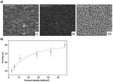 | ||
| Fig. 1 (a) SEM images of freshly etched porous silicon matrices. Scale bars are 500 nm. The samples (i), (ii), and (iii) were etched at 5.7 mA cm−2, 28.4 mA cm−2 and 56.8 mA cm−2, respectively. (b) Graph of the variation in the calculated porosity versus the current density. The error bars were calculated after taking six measurements. The line corresponds to the exponential fit. | ||
The IRS spectrum from the pSi films was also collected. The spectra display fringes, which result from Fabry–Pérot interferences at the two boundaries of the pSi layer. The position of the fringe maxima is given by the following relationship:
| mλ = 2nL | (1) |
Chemical modification and characterization
The surface of the freshly etched pSi samples was modified in order to graft PNIPAM. Three different paths for functionalizing the surface were tested in order to study the effect of surface functionalization on the behavior of grafted PNIPAM and to identify the best condition for developing a sensor for temperature change. Fig. 2 describes the three different pathways used to introduce PNIPAM within nanostructured pSi. The surfaces modified by path A and path B were thermally oxidized and ozone oxidized, respectively, prior to the attachment of the ATRP initiator and prior to the polymerization of the NIPAM onto the surface of the pSi. In contrast, path C involved hydrosilylation of undecylenic alcohol before initiator attachment and polymerization.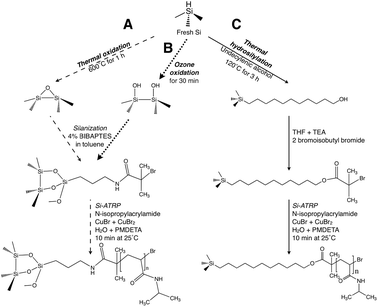 | ||
| Fig. 2 Schematic of PNIPAM grafting onto the pSi surface. Three different pathways were investigated. Path A: the pSi samples were thermally oxidized at 600 °C for 1 h, followed by the silanization with 4% of BIBAPTES in toluene and the Si-ATRP polymerization process of NIPAM performed at 25 °C for 10 min. Path B: samples are oxidized by ozone for 30 min, the silanization and the polymerization process were identical to path A. Path C: hydrosilylation of the undecylenic alcohol for 3 h at 120 °C was performed on the freshly etched samples, then the surface was reacted with 2-bromoisobutyl bromide, followed by NIPAM polymerization at 25 °C for 10 min. | ||
The pSi samples were characterized by FTIR spectroscopy in the ATR mode after every functionalization step. The FTIR characterization of the pSi sample modified by path A was recently described by Vasani et al.25 Very similar results were obtained here (see S1 in ESI†). The FTIR spectra of the samples modified by paths A and B presented the characteristic vibration bands of the PNIPAM after exposure of the surface modified with the initiator to the NIPAM, indicating that successful grafting was realized. FTIR spectra of the surfaces modified according to path C are presented in Fig. 3 for (a) a pSi surface functionalized with undecanol through hydrosilylation of undecylenic alcohol, (b) the previously undecanol-functionalized pSi surface after reaction with the initiator 2-bromoisobutyl bromide and (c) after NIPAM polymerization. In spectrum (a) bands at 1459, 2924 and 2853 cm−1 were assigned to the deformation and stretching (symmetric and asymmetric) vibrational modes of the aliphatic C–H groups, respectively. The presence of bands at 907 and 2090 cm−1, assigned to the Si–H2 bending mode and to the Si–Hx stretching mode, respectively, indicates that part of the silicon hydride remained unreacted at the pSi surface.26 Spectrum (a) also exhibited a band at 1386 cm−1, assigned to the O–H deformation vibrational mode or to the CH2 wagging vibrational mode, which appears in the same region, and a broad band at 3434 cm−1, assigned to the stretching vibrational mode medium-strong hydrogen bonds with adsorbed water. In addition, the band at 1073 cm−1 assigned to the Si–O stretching vibrational mode attests the presence of silicon oxide at the surface of pSi that forms as a side reaction during thermal hydrosilylation, even if the reaction was performed under an inert atmosphere.
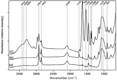 | ||
| Fig. 3 FTIR-ATR spectra of the pSi surface modified following path C, (a) after the hydrosilylation of undecylenic alcohol, (b) after grafting the initiator to the surface and (c) after polymerization of NIPAM. | ||
After the reaction between the 2-bromoisobutyl bromide and the undecanol-functionalized pSi surface, a band was observed in spectrum (b) at 1726 cm−1 corresponding to the ester group, confirming the successful grafting of the initiator to the surface.
After the polymerization reaction, bands were observed in spectrum (c) at 1641 and 1536 cm−1 corresponding to the amide I and amide II bands, respectively, indicating the presence of the PNIPAM on the pSi surface. The large broad band formed at 3380 cm−1 is associated with the N–H stretching vibrational mode from the amide functions on PNIPAM. The sharp band at 3282 cm−1 was assigned to the hydrogen bonded O–H (intermolecular) stretching vibration, characteristic of a polymer. Bands at 1367 cm−1 and 1386 cm−1 were attributed to the asymmetrical deformation of the isopropyl group of the PNIPAM. The strong band at 1033 cm−1 was assigned to the Si–O stretching vibrational mode. Finally, bands were observed at 1459, 2852 and 2924 cm−1 due to the C–H vibrational modes (deformation and stretching, respectively). FTIR data therefore confirm the presence of the PNIPAM on the pSi surface.
The IRS spectra from the thin film modified with the initiator and modified with the PNIPAM for the 3 paths tested were collected in air and analyzed by the transfer matrix method to calculate pore filling. The value of the refractive indices used for PNIPAM was 1.45.27 The results of the calculations of the pore filling with PNIPAM are presented in Fig. 4a for the three chemical paths and the six current densities investigated in this study. Except for the sample etched at 5.7 mA cm−2, a decrease in the value of the pore filling was observed with increase in current density, for all three surface chemistries tested. An average of 97.8%, 92.6% and 86.4% of PNIPAM inside the pores was measured for the pSi etched at 2.8 mA cm−2 and modified by paths A, B and C, respectively. An average of 74.6%, 60.0% and 42.5% of PNIPAM inside the pores was measured for the pSi etched at 56.8 mA cm−2 and modified by paths A, B and C, respectively. The difference in pore filling observed for the different etching conditions can be explained by the fact that the thickness of the grafted polymer layer was similar for all etching conditions, the average pore sizes of the starting material increased with increasing current density.
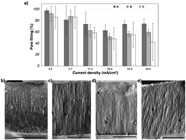 | ||
| Fig. 4 (a) Pore filling calculated for all the different etching conditions, after modification of the surface by the three different paths previously described. The histograms A, B and C correspond to the sample modified by thermal oxidation and polymerization (path A), ozone oxidation and polymerization (path B) and thermal hydrosilylation and polymerization (path C), respectively. (b) SEM cross-section view of pSi freshly etched at 28.4 mA cm−2. (c) SEM cross-section view of pSi etched at 28.4 mA cm−2 and modified with path A. (d) SEM cross-section view of pSi etched at 28.4 mA cm−2 and modified with path B. (e) SEM cross-section view of pSi etched at 28.4 mA cm−2 and modified with path C. Scale bars = 2 μm. The arrows indicate the presence of the polymer inside pores. | ||
It is also conceivable that pore filling changes with depth in the porous layer. However, we did not find any evidence for this. SEM cross sections were acquired in the high vacuum mode for a freshly etched sample at 28.4 mA cm−2 (Fig. 4b), a sample etched with the same current density and subsequently modified by path A (Fig. 4c), a sample etched at 28.4 mA cm−2 and modified by path B (Fig. 4d) and finally a pSi film etched at 28.4 mA cm−2 and modified by path C (Fig. 4e). Judging from the difficulty to distinguish the pores after modification of the surface with the PNIPAM in all the three cases and from the absence of a pore filling gradient along the depth, we can conclude that the polymer filled the pores and confirm the results calculated by the IRS spectra from the thin films (Fig. 4a). In addition, nitrogen adsorption measurements performed on samples etched at 5.7 mA cm−2, 28.4 mA cm−2 and 56.8 mA cm−2, and chemically modified by paths A, B and C showed that mesoporosity disappeared after the polymerization step for all the tested conditions (data not shown). This observed gap in results between the pore filling calculations and the N2 volumetry can be explained by the fact that porosity may still be present in the samples but hidden by a thin polymer layer at the external surface of the pSi films, and therefore not accessible to nitrogen during the volumetry analysis.
The difference in the pore filling observed for the three surface functionalizations (Fig. 4a) can be explained as follows: for paths A and B, the pSi surface was modified by oxidation, involving the insertion of oxygen atoms inside the silicon walls. This phenomenon is known to cause expansion of the wall thereby reducing the volume available inside the pores.28 Therefore, if the volume available decreases, the amount of polymers required for filling the pore is smaller, and the pore filling occurs at higher current density compared to the sample modified by hydrosilylation.
Optical sensing
The hybrid pSi-PNIPAM hybrid materials were exposed to milliQ water at 25 °C and at 50 °C in a customized flow cell and IRS spectra were collected as a function of time. These temperature values were chosen to be well below and well above the LCST (32 °C) of the PNIPAM. As described previously, the PNIPAM displays thermoresponsive properties: beyond its LCST, the polymer becomes less soluble and collapses.14,16,29The IRS spectrum of the pSi/NIPAM samples etched at 56.8 mA cm−2 is presented as an example in Fig. 5 (inset). Conspicuous variations in the position and in the amplitude of the interference fringes were noted after introducing the water at 50 °C (dashed line spectrum). As described previously and consistent with the literature,6,21 the FFT of the spectrum gives a peak whose position corresponds to the value of 2nL in the Fabry–Perot relationship (eqn (1)). Fig. 5a and b depict changes in the 2nL value and changes in the amplitude of the FFT, respectively, for pSi-PNIPAM hybrids measured upon thermal change between 25 °C and 50 °C. The three plots correspond to the samples modified with the three different surface chemistries shown in Fig. 2, for the six different pore sizes, indicated in Table 1. All of the six films displayed a temperature-dependent optical thickness shifts for all three surface chemistries (Fig. 5a). In all cases, the shift of the 2nL value was fully reversible. No significative change was observed for pSi samples not grafted with PNIPAM. The magnitude of the change in the 2nL value during thermal increase (25°C to 50°C) decreased slightly with a measured shift in 2nL of 0.02%, 0.009%, 0.06%, 0.06%, 0.05%, 0.09% for current densities of 2.8 mA cm−2, 5.7 mA cm−2, 11.4 mA cm−2, 28.4 mA cm−2, 42.6 mA cm−2 and 56.8 mA cm−2 respectively (data not shown). For the pSi–PNIPAM hybrids modified following path A (Fig. 5a plot A): the magnitude of the shift of the 2nL value during thermal increase (25°C to 50°C) became more pronounced as the current densities used (and therefore the porosities and pore sizes of the pSi film) increased, with a measured shift in 2nL of 0.1%, 0.14%, 0.28%, 0.29%, 0.41% and 0.95% for current densities of 2.8 mA cm−2, 5.7 mA cm−2, 11.4 mA cm−2, 28.4 mA cm−2, 42.6 mA cm−2 and 56.8 mA cm−2 respectively.
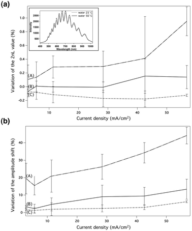 | ||
| Fig. 5 Variation in the (a) 2nL value and the (b) FFT intensity measured by IRS for pSi-NIPAM hybrids etched at 2.8 mA cm−2, 5.7 mA cm−2, 11.4 mA cm−2, 28.4 mA cm−2, 42.6 mA cm−2 and 56.8 mA cm−2, and exposed to temperature variation (from 25 °C to 50 °C). Plots A, B and C correspond to the pSi-PNIPAM hybrid modified by path A, path B and path C, respectively. Inset: the IRS spectrum of the pSi-NIPAM etched at 56.8 mA cm−2 modified with path A at 25 °C (full line spectrum) and with path A at 50 °C (dash line spectrum). | ||
The positive and reversible shift observed for the surfaces modified following path A was consistent with our earlier work, and can be explained by an increase in the refractive index inside the pores upon heating.25 Indeed, Garner et al. studied the change in refractive index during the volume-phase transition of the PNIPAM hydrogel micro-spheres by optoelectronics and bio-photonics.30 The authors demonstrated that the refractive index of PNIPAM increased from 1.32 to 1.39 when the temperature was varied from below the critical temperature to above the critical temperature. Furthermore, during the coil-to-globule transition of PNIPAM, grafted polymer chains extending into the bulk water at low temperature are retracted into the pSi layer at the LCST, therefore replacing water in the pores with polymer component and leading to a further increase in refractive index of the porous layer.
The observed differences in the magnitude of the positive 2nL shift during thermal cycling for the pSi-PNIPAM hybrids modified following path A at different current densities require further explanations. For small current densities, pores are small and filled almost completely with PNIPAM (Fig. 4a), placing some constraints on the polymer and possibly reducing the ability of the polymer to switch conformation. As pore size increases and filling of pores with PNIPAM decreases, these constraints are lifted and a greater conformational change in the polymer chains can occur upon thermal cycling.
In contrast, the pSi-PNIPAM hybrid modified using path B displayed barely no shift in the 2nL value during thermal cycling until pores exceeded a certain size threshold (at current densities higher than 28.4 mA cm−2). From 28.4 mA cm−2 onwards, an increase in the 2nL value was observed. At the highest current density used, the shift in 2nL was 0.14%. The increase in the 2nL value starting from the samples etched at high current densities was attributed to an increase in refractive index inside the pores as described for the samples modified using path A. The absence of significant shift of the 2nL value for samples etched at lower current densities than 28.4 mA cm−2 can be explained by considering the large percentage of pore filling in these cases (Fig. 4a). At the same time, the silanol density of the ozone oxidized surface (Path B) is expected to be higher than that on the thermally oxidized surface (path A),15 which would translate into a higher density of the BIBAPTES initiator and hence a higher grafting density of PNIPAM which might force the system to behave more like a hydrogel (vide infra).15
Finally, we observe a slight decrease in the magnitude of the 2nL value during thermal increase for the sample modified with path C (plot C). As the current density of the template increased, the magnitude of the change in the 2nL value increased slightly, with a measured shift in 2nL of 0.07%, 0.08%, 0.12%, 0.17%, 0.18% and 0.13% for current densities of 2.8 mA cm−2, 5.7 mA cm−2, 11.4 mA cm−2, 28.4 mA cm−2, 42.6 mA cm−2 and 56.8 mA cm−2, respectively.
Two hypotheses can be proposed for explaining the decrease in the 2nL value observed during thermal cycling for the pSi-PNIPAM hybrids modified following path C. The first hypothesis proposed is in relation to the work of Segal et al., where the authors infiltrated a PNIPAM hydrogel into a pSi film previously oxidized at 800 °C.15 And they observed a decrease in optical thickness at the temperature attributed to the volume phase transition of the PNIPAM hydrogel. The authors explained the decrease on the basis that the hydrogel held above the LCST in the confined environment of the pores exerts a compressive stress on the pSi film, resulting in a decrease in the depth of the porous layer as the polymer chains collapse. Following this line of thought, it is conceivable that PNIPAM grafted on the pSi samples modified by hydrosilylation (path C), behaves more like a hydrogel, perhaps due to a higher grafting density compared to the pSi modified following path A or B. Unfortunately, it is impossible to accurately determine the graft density of polymer brushes within the porous layer.
The second hypothesis invokes the hydrophobicity of the surface. The samples modified by path C contain a long carbon chain, providing a hydrophobic surface layer, in contrast to the samples modified by the path A or B which contain a more hydrophilic linker. Since PNIPAM becomes hydrophobic above its LCST the decrease in the 2nL value for the pSi-PNIPAM hybrids modified following path C upon heating could be explained in terms of expulsion of water from the linker-polymer layer inside the pores resulting in a net decrease in refractive index of the porous matrix, which outweighs the increase in the refractive index of the PNIPAM.14,16,30
Comparing the performance of the pSi-PNIPAM hybrids according to the optical thickness variation upon thermal variation, the greatest response was obtained for the pSi-PNIPAM hybrid etched at 56.8 mA cm−2 and modified following path A.
Fig. 5b depicts the variations in the amplitude of the FFT peak for the different current densities and the three surface modifications. Pacholski et al. described the reflectance spectra calculation using a simple double-layer Fabry Perot interference model.21 This model can be applied in our study, considering the pSi-PNIPAM hybrid as a first layer with a PNIPAM layer outside of the porous layer on top of it, generating three interfaces: water–PNIPAM, PNIPAM–(pSi–PNIPAM) and (pSi–PNIPAM)–Si bulk. The FFT amplitude of the interference spectrum is correlated with the index contrast at each interface. An increase in the FFT amplitude was observed for all the hybrid samples produced during the temperature change across the LCST. However, the magnitude of the shift increased with increasing current density for all three surface modifications. The variation in the magnitude of the amplitude change was the most pronounced for path A increasing from 19.51% to 44.15%. Recently, the group of Cunin demonstrated that as the thickness of either layer increases, the amplitude of the FFT peak exhibits a damped oscillatory function. The authors explained that the magnitude of this oscillation scales with the refractive index of the coating layer. The amplitude of the oscillation therefore allows for monitoring of the evolution of the layer.31 The increase in amplitude of the FFT peak observed during thermal increase from 25 °C to 50 °C was attributed to the change in PNIPAM layer thickness and a decrease in the index contrast at the interface. In fact, the refractive index of the PNIPAM increased when the temperature was above the LCST, leading to a reduced index contrast,37 and we have previously shown that a grafted PNIPAM layer on silicon collapses upon transitioning above the LCST, leading to a decreased layer thickness.32
Conclusions
Hybrid pSi–PNIPAM films were prepared by the SI-ATRP polymerization process onto the internal and the external surface of pSi using three different surface functionalization pathways. For the three different surface chemistries tested, six different porosities of pSi were prepared, in order to investigate the behavior of the polymer inside the pores and to identify the largest optical response to temperature change. Depending on the surface modification and the porosity of the hybrids, two major responses were observed. A slight decrease in the 2nL value was noted for the small pores or the pores modified by hydrosilylation (path C), maybe due to the high grafting density of the polymer and/or to the hydrophobicity of the surface, influencing the refractive index of the porous matrix during the swelling of the PNIPAM at the LCST. On the other hand, a positive shift of the 2nL value was observed upon heating for the samples containing large pores modified by ozone oxidation and for all samples functionalized by thermal oxidation. This optical response was attributed to the collapse of the polymer layer, leading to an increase in the polymer concentration inside the pores, increasing the refractive index of the porous matrix.Thermal oxidation of highly porous Si followed by silanization and SI-ATRP gave the largest response in terms of 2nL shift as a result of a temperature change around the LCST. The high porosity of the films rendered the polymer more flexibile and generated a larger signal. This surface gave the best response with respect to a change in optical thickness. In the future, this surface functionalization approach could be transferred to a photonic pSi structure such as a Bragg mirror or a rugate filter, causing a color change in the pSi film in response to temperature changes, which could be integrated into a wound dressing. This system may eventually enable the detection of a temperature change from a physiological to a pathological level in the wound bed, and enable monitoring by the unaided eye.
Experimental
pSi preparation
pSi films were prepared by the electrochemical etching of highly doped, (100)-oriented, boron doped p++ Si wafers (0.00055–0.001 Ω cm resistivity) (Siltronix, France) in a 1:1 (48%) aqueous hydrofluoric acid (HF)/ethanol solution (Fisher Scientific). The etching process was performed in a Teflon cell with a platinum electrode and a computer-controlled galvanostat (Keithley 2425). Prior to formation of the sensing pSi layer, the silicon wafer underwent a pre-treatment in order to inhibit the formation of a parasitic surface layer during the etch.23 The wafer with an exposed area of 1.76 cm2 was first etched using a current density of 28.4 mA cm−2 for 30 seconds, and then exposed to a 0.1 M NaOH solution for two minutes. The chip was exposed to a HF:ethanol (1:1 volume ratio) solution and then rinsed three times with ethanol and dried under a stream of nitrogen. The pre-treated silicon wafer was then etched at different constant current densities and times, described in Table 1. The pSi samples were rinsed 3 times with ethanol and dried under a stream of nitrogen gas.
Chemical functionalization: three different surface functionalizations to introduce PNIPAM within nanostructured pSi were explored (Fig. 2). Path A: after etching, thermal oxidation was performed in a Labec tube furnace (Laboratory Equipment Pty. Ltd.), at 600 °C for 1 hour, generating SiO bonds at the surface.33 Silanization reaction was carried out in a 4% solution of 3-(2-bromoisobutyramido)propyl(triethoxy)silane (BIBAPTES) in freshly distilled toluene for 1 h, to immobilize the initiator. The BIBAPTES was synthesized following a published procedure.25 After the silanization reaction, the samples were rinsed with ethanol and dried under a stream of nitrogen gas. Surface initiated atom transfer radical polymerization (SI-ATRP) of N-isopropylacrylamide (NIPAM) (recrystallized, Aldrich) was carried out by immersing the silanized pSi sample in a monomer solution consisting of 10% w/v NIPAM, 0.5% w/v CuBr (Sigma), 0.1% w/v CuBr2 (Sigma) and 1.5% w/v PMDETA (99%, Aldrich) in Milli-Q water (18.2 MΩcm, Labconco). Nitrogen was continuously bubbled through the reaction solution to expel oxygen. Polymerization was performed in a scintillation vial fitted with a modified screw-on cap for the introduction and escape of nitrogen gas. The reaction was performed at 25 °C for 10 min. Once the reaction was complete, the pSi samples were rinsed thoroughly with Milli-Q water and dried under a stream of nitrogen gas. Path B: after etching, the samples were oxidized by ozone for 30 min in order to generate silanol groups on the surface of the sample.34 Silanization and the polymerization were carried out as described for path A.
Path C: after etching, the samples were thermally hydrosilylated with undecylenic alcohol at 120 °C for 3 h under argon, to introduce hydroxyl groups on the surface. Then the samples were reacted with 5% w/v 2-bromoisobutyl bromide, 5% w/v triethylamine, in tetrahydrofuran (THF) for 1 h at room temperature to introduce the polymerization initiator. The samples were rinsed with THF and ethanol and dried under a stream of nitrogen before performing NIPAM polymerization by SI-ATRP as described previously. Once the reaction was complete, the pSi samples were rinsed thoroughly with Milli-Q water and dried under a stream of nitrogen gas.
Scanning electron microscopy (SEM)
SEM images were obtained on a FEI QuantaTM 450 Field Emission Gun Environmental Scanning Electron Microscope. The pSi samples were coated with a thin (3 nm) layer of platinum to prevent charging. A spot size of 3.0 mm and an accelerating voltage of 15.0 kV were used to obtain the images in the high vacuum mode.Fourier transform infrared (FTIR) spectroscopy
FTIR spectroscopy was performed with a Nicolet iN10 microscope (Thermo scientific) coupled to the liquid nitrogen cooled Mercury–cadmium–telluride (MCT) detector, in the attenuated total reflectance (ATR) mode. Background spectra were taken in air and all spectra were recorded with an aperture size of 3 mm, over the range of 650–3800 cm−1, at a resolution of 22 cm−1 averaging 64 scans.Nitrogen adsorption–desorption experiments
Nitrogen adsorption–desorption isotherms of the pSi films were recorded at 77 K using a Micromeritics ASAP 2020 volumetric apparatus. Prior to the adsorption experiment, the samples were outgassed overnight in situ at 298 K. The surface area of the sample was measured by the BET (Brunauer–Emmett–Teller) method, which yields the amount of adsorbates corresponding to a molecular monolayer.35,36 The pore dimensions were determined by using the BdB (Broekhof–de Boer) method from the nitrogen adsorption curve.37 The mesoporous volume was measured as the adsorbed volume at the top of the capillary condensation step of the isotherm. The specific surface area of the porous matrix and the porous volume were expressed per geometrical unit area of the pSi sample.Interferometric reflectance spectral measurements (IRS)
White light from a tungsten lamp (Ocean Optics) was fed through one end of a bifurcated fiber-optic cable and focused through a lens onto the surface of the pSi film at normal incidence. The light source was then focused onto the center of the sample surface with a spot size approximately 1 mm in diameter. Light reflected from the film was collected through the same optics, and the distal end of the bifurcated fiber optic cable was connected to a CCD spectrometer (Ocean Optics S-2000). Reflectivity spectra were recorded in the wavelength range of 400–1000 nm, with a spectral acquisition time of 0.1 s. Typically 50 spectral scans (5 s total integration time) were averaged. A Fast Fourier Transform (FFT) using an algorithm from the Wavemetrics Inc. (www.wavemetrics.com) IGOR program library was applied to the resulting spectrum according to the previously published procedure.31Experiments were carried out in a custom-made aqueous flow cell at room temperature. The samples were immersed in water of controlled temperature, and the temperature of the water was measured using a thermocouple. The water was introduced at a flow rate of 100 μL min−1. The samples were monitored at 25°C for 10 min, then the temperature was raised to 50 °C for 10 min, followed by perfusion of 25 °C water through the flow cell for 10 min. Interference spectra were collected in 1 minute intervals. The data displayed are the average of six replicates for each condition.
Thickness and porosity calculations
The optical parameters (thickness, porosity and refractive index) were obtained by performing a best-fit calculation of the reflectance spectrum, by means of a simulation program (SCOUT, obtained from M. Theiss Hard- and Software) that is based on the transfer matrix method.38 The software generates the theoretical reflectance spectrum of the pSi film, calculating its effective refractive index using the dielectric function of bulk silicon and using a Bruggeman effective medium approximation.39 Porosity and thickness are the two free parameters of the model; their value is adjusted in a least-squares algorithm in order to obtain the best fit between the experimental and the calculated spectra.Pore filling calculation
The pore filling was calculated using the transfer matrix method from the program SCOUT, previously described. In order to obtain a best fit between the experimental reflectance spectrum and the theoretical reflectance spectra, the refractive index of the polymer, the pore filling and the thickness of the polymer layer were added to the previous parameters (thickness, porosity and refractive index of the porous layer). The experimental spectra were recorded in air. The model generates the theoretical reflectance spectrum of the pSi-PNIPAM film, calculating its effective refractive index using the dielectric function of the bulk silicon, of the polymer and applying a Bruggeman effective medium approximation.Acknowledgements
The authors would like to thank the Wound Management Innovation CRC (Australia) for providing funding for this work.Notes and references
- L. T. Canham, Appl. Phys. Lett., 1990, 57, 1046–1048 CrossRef CAS.
- A. G. Cullis and L. T. Canham, Nature, 1991, 353, 335–338 CrossRef CAS.
- M. P. Stewart and J. M. Buriak, Adv. Mater., 2000, 12, 859–869 CrossRef CAS.
- A. Jane, R. Dronov, A. Hodges and N. H. Voelcker, Trends Biotechnol., 2009, 27, 230–239 CrossRef CAS.
- N. H. Voelcker, I. Alfonso and M. R. Ghadiri, ChemBioChem, 2008, 9, 1776–1786 CrossRef CAS.
- C. Pacholski, C. Yu, G. M. Miskelly, D. Godin and M. J. Sailor, J. Am. Chem. Soc., 2006, 128, 4250–4252 CrossRef CAS.
- M. Sailor and J. R. Link, Abstr. Paper. Am. Chem. Soc., 2003, 226, U348–U348 Search PubMed.
- V. S. Y. M. Lin, K. Dancil, K. S. Sailor, M. J. Ghadiri and M. R. Ghadiri, Science, 1997, 278, 840–843 CrossRef CAS.
- M. M. Orosco, C. Pacholski, G. M. Miskelly and M. J. Sailor, Adv. Mater., 2006, 18, 1393–1396 CrossRef CAS.
- M. Calvin, Wounds, 1998, 10, 12–32 Search PubMed.
- K. Harding, Available from: http://www.wuwhs.org/datas/2_1/10/Diagnostic_3M_English_WEB.pdf.
- M. Fierheller and R. G. Sibbald, Adv. Skin Wound Care, 2010, 23, 369–379 Search PubMed.
- L. A. Perelman, T. Moore, J. Singelyn, M. J. Sailor and E. Segal, Adv. Funct. Mater., 2010, 20, 826–833 CrossRef CAS.
- J. S. Scarpa, D. D. Mueller and I. M. Klotz, J. Am. Chem. Soc., 1967, 89, 6024 CrossRef CAS.
- E. Segal, L. A. Perelman, F. Cunin, F. Di Renzo, J. M. Devoisselle, Y. Y. Li and M. J. Sailor, Adv. Funct. Mater., 2007, 17, 1153–1162 CrossRef CAS.
- R. B. Vasani, M. A. Cole, A. V. Ellis and N. H. Voelcker, in Nanomaterials for life Sciences: Polymeric Nanomaterials, ed. S. S. R. K. ChallaWiley-VCH, 2010 Search PubMed.
- H. G. Schild, Prog. Polym. Sci., 1992, 17, 163–249 CrossRef CAS.
- B. M. Baysal and F. E. Karasz, Macromol. Theory Simul., 2003, 12, 627–646 CrossRef CAS.
- R. Barbey, L. Lavanant, D. Paripovic, N. Schuwer, C. Sugnaux, S. Tugulu and H. A. Klok, Chem. Rev., 2009, 109, 5437–5527 CrossRef CAS.
- Y. Arita and Y. Sunohara, J. Electrochem. Soc., 1977, 124, 285–295 Search PubMed.
- C. Pacholski, M. Sartor, M. J. Sailor, F. Cunin and M. G. Miskelly, J. Am. Chem. Soc., 2005, 127, 11636–11645 CrossRef CAS.
- M. Theiss, Dr Bernhard Klein Str. 110 D-52078 Aachen, Germany, http://www.wtheiss.com/.
- B. Sciacca, E. Secret, S. Pace, P. Gonzalez, F. Geobaldo, F. Quignarda and F. Cunin, J. Mater. Chem., 2011, 21, 2294–2302 RSC.
- C. F. Bohren and D. R. Huffman, Wiley, New York, 1983, 217 Search PubMed.
- R. B. Vasani, S. J. P. McInnes, M. A. Cole, A. M. M. Jani, A. V. Ellis and N. H. Voelcker, Langmuir, 2011, 27, 7843–7853 CrossRef CAS.
- R. Boukherroub, J. T. C. Wojtyk, D. D. M. Wayner and D. J. Lockwood, J. Electrochem. Soc., 2002, 149, H59–H63 CrossRef CAS.
- T. Kanai, D. Lee, H. C. Shum and D. A. Weitz, Small, 2010, 6, 807–810 CrossRef CAS.
- E. J. Anglin, M. P. Schwartz, V. P. Ng, L. A. Perelman and M. J. Sailor, Langmuir, 2004, 20, 11264–11269 CrossRef CAS.
- M. D. Kurkuri, M. R. Nussio, A. Deslandes and N. H. Voelcker, Langmuir, 2008, 24, 4238–4244 CrossRef CAS.
- B. W. Garner, T. Cai, S. Ghosh, Z. Hu and A. Neogi, Appl. Phys. Express, 2009, 2, 057001 Search PubMed.
- S. Pace, B. Seantier, E. Belamie, N. Lautredou, M. J. Sailor, P.-E. Milhiet and F. Cunin, Langmuir, 2012, 28, 6960–6969 Search PubMed.
- M. A. Cole, N. H. Voelcker, H. Thissen, R. G. Horn and H. J. Griesser, Soft Matter, 2010, 6, 2657–2667 RSC.
- V. Petrova Koch, T. Muschik, A. Kux, B. K. Meyer, F. Koch and V. Lehmann, Appl. Phys. Lett., 1992, 61, 943–945 CrossRef CAS.
- E. J. Anglin, L. Y. Cheng, W. R. Freeman and M. J. Sailor, Adv. Drug Delivery Rev., 2008, 60, 1266–1277 CrossRef CAS.
- P. H. E. Stephen Brunauer and E. Teller, J. Am. Chem. Soc., 1938, 60, 309–319 CrossRef CAS.
- S. J. Gregg and K. S. W. Sing, Adsorption, Surface Area and Porosity, Academic Press Inc., London, 1982 Search PubMed.
- J. H. de Boer and J. C. P. Broekhoff, J. Catal., 1968, 10, 377–390 CrossRef CAS.
- M. Born and E. Wolf, Principles of Optics: Electromagnetic Theory of Propagation, Interference and Diffraction of Light, 7th edn, Cambridge University Press, New York, 1999, p. 952 Search PubMed.
- C. F. Bohren and D. R. Huffman, Adsorption and scattering of light by small particles, Wiley, New York, 1983 Search PubMed.
Footnote |
| † Electronic supplementary information (ESI) available. See DOI: 10.1039/c2nj40693d |
| This journal is © The Royal Society of Chemistry and the Centre National de la Recherche Scientifique 2013 |