Optofluidic imaging: now and beyond
Yanhui
Zhao
,
Zackary S.
Stratton
,
Feng
Guo
,
Michael Ian
Lapsley
,
Chung Yu
Chan
,
Sz-Chin Steven
Lin
and
Tony Jun
Huang
*
Department of Engineering Science and Mechanics, The Pennsylvania State University, University Park, PA 16802, USA. E-mail: junhuang@psu.edu
First published on 9th November 2012
Abstract
More than a decade of research work in optofluidics has yielded a large catalogue of optofluidic elements that can manipulate light at the micro-scale (e.g., lenses, prisms). Although these elements have proven useful for many on-chip processes (e.g., miniaturized flow cytometry, interferometry and sample spectroscopy), certain deficiencies have precluded their use in micro-scale imaging. However, recent work in optofluidic imaging has avoided optofluidic elements entirely and focused instead on image capture and composition techniques, demonstrating impressive resolution in both 2D imagery and 3D tomography. In this Focus article, we will discuss some of the recent successes in optofluidic imaging and will expound our expectations for the near future of the optofluidic imaging discipline.
1. Introduction
Optical imaging is defined as the use of light to capture and preserve data about an object's appearance and physical structure. Its origin can be traced back over two thousand years when the first “pinhole experiment” was documented in China, yet it remains a thriving discipline with many applications in modern technology, from entertainment to consumer electronics to scientific research to medical diagnostics. Over the last decade and a half, much academic and industry attention has been directed at miniaturizing optical imaging devices. Making the devices small aims to achieve portability (easily move a device from one location to another), manoeuvrability (easily change the orientation or configuration of a device) and low cost. Miniaturized imaging devices have already found applications in personal electronics (e.g., cameras, cell phones, tablets), in vivo bio-imaging devices, such as endoscopes, surveillance/security systems, miniaturized microscopes and point-of-care diagnostics.1–3Optical imaging systems require precise fabrication, alignment and actuation of various optical components. This is a challenging enough task at the traditional scale, and has proven to be only more difficult within the constraints enforced by the extremely limited space of miniaturized systems. Thus, in recent years researchers have been seeking new approaches to the miniaturization of optical imaging systems.
In their efforts to miniaturize optical imaging systems, academics turned to the discipline of microfluidics.4–6 Years of research effort have yielded a large catalogue of clever microfluidic devices and elements that can manipulate light at the micro-scale—a discipline now termed optofluidics.7,8 Some of these elements manipulate light traveling in the device plane,9–11 some manipulate light traveling perpendicular to the device plane12–14 and others serve to redirect light from a perpendicular path of travel into the device plane.15,16 To provide the reader with important examples of optofluidic elements, this article examines four representative elements: a laser, a lens, a prism and a switch.
Optofluidic elements have proven useful for manipulation of light in on-chip processes, such as flow cytometry,17,18 interferometery19 and sample spectroscopy.20 However, it has also been observed that these elements suffer deficiencies that make them difficult to use for imaging purposes. This Focus article will discuss the deficiencies of optofluidic elements (e.g., lenses, prisms) for imaging, and will examine recent approaches to imaging at the micro-scale that have yielded promising results. Finally, this article will conclude with our perspective for the near future of optofluidic imaging and how it stands to make a realistic impact on biomedicine.
2. Optofluidic elements
Over the last decade, the combined efforts of many research groups around the world have yielded a large collection of optofluidic elements. These elements use fluids to manipulate light at the micro-scale, accomplishing the function of their macro-scale counterparts, only on a small microfluidic chip. Some elements have taken the shape of their macro-scale counterparts (like a fluidic lens with the two-dimensional shape of a traditional glass lens21), while others have used configurations different from their macro-scale counterparts (like a fluidic lens that relies on the diffusive gradient of refractive index between two laminar flow streams22). To provide the reader with important examples of optofluidic elements, in this section we highlight four optofluidic elements. These highlighted elements are representative examples of the macro-scale counterparts whose effects they mimic: an optofluidic laser, an optofluidic prism, an optofluidic switch and an optofluidic lens.Fig. 1A shows an interesting example of an optofluidic laser, developed by the Whitesides group.23 It uses a straight-line microfluidic channel that contains three laminar flow streams, with two streams of low-refractive-index fluid sandwiching a stream of high-refractive-index fluid; the inner stream is termed the core flow, and the two outer streams are termed the cladding flows. The core fluid contains dissolved fluorescent dye (rhodamine 640 perchlorate was used in the demonstration of the element) and the two ends of the straight-line channel are coated with thin sheets of gold, with the coating at one end of the channel being less thick than the coating at the other end (thickness of 100 nm and 40 nm were used, as indicated in Fig. 1A).
 | ||
| Fig. 1 (A) An optofluidic laser. An illumination source excites fluorescent dye in the optically pumped region, and the resulting fluorescence is largely contained in the optical cavity by two low-refractive-index cladding flows and two thin gold coatings. (B) An optofluidic prism. The shape of the prism is tuned by changing the three flow rates into the triangular chamber, which in turn steers the incident light beam. (C) An optofluidic switch. Air-filled microfluidic channels act as mirrors to incident light; the channels are collapsed by increasing fluid pressure in an adjacent microfluidic channel, thus permitting light to pass through. (D) An optofluidic lens. Two cladding flows of low refractive index sandwich a central flow of high refractive index in a microfluidic channel, causing light sent through the channel to be focused. By changing the flow rates of the cladding and central flows, the light focal point can be made to swing horizontally within the device plane. Images reproduced from ref. 15, 22, 23, 24, 25. | ||
When the fluorescent dye in the straight-line channel is excited by an external excitation source, the resulting fluorescence travels back and forth within the straight-line channel, being largely contained by the waveguide created by the two cladding flows of lower refractive index, and being reflected at the channel ends by the gold coatings. The primary path of escape for the fluorescence is the channel end with the thinner gold coating. Thus, the straight-line channel represents an optical cavity in which the fluorescent dye is optically pumped, forming a laser. The laser is a configurable system, where changing of the dye, solvent composition and/or stream flow rates can adjust the emission wavelength, numerical aperture, absorbance and modal content of the laser. Thus, the laser serves to take off-chip light—the external excitation source—and convert it to a controllable light beam in the chip plane.
Fig. 1B shows a configurable optofluidic prism that was reported in 2011.24 The prism is formed by the convergence of three laminar flow streams in a triangular-shaped chamber, two of which are of the same fluid. A refractive index difference between the two fluids causes incident light to be refracted at the fluid interfaces, thus steering the light path on-chip in the same way as a macro-scale prism. The shape of the fluid prism can be controlled by adjusting the three flow rates that feed into the triangular chamber, altering the prism's apex angle, as well as changing it from a symmetric shape to an asymmetric one. Thus, this optofluidic prism can, by means of changing its shape, provide a continuous adjustment to a light beam's path.
Fig. 1C shows a tunable optofluidic 2 × 2 switch, developed by the Psaltis group and reported in 2011.25 The operating mechanism of the switch centers on an air-filled microfluidic channel in a PDMS device. The refractive index of PDMS is ∼1.412, while the refractive index of air is ∼1. Considering these values, the critical angle for total internal reflection of light incident on the PDMS–air interface is 45.1°. By orienting the air-filled channel to a light source at an angle slightly above the critical angle, all light incident on the air-filled channel is reflected. Another microfluidic channel is situated immediately adjacent to, and parallel to, the air-filled channel. This adjacent channel is filled with fluid with a refractive index matched to that of the surrounding PDMS. This fluid is then controlled pneumatically (off-chip, by an electromagnetic valve), such that when pneumatic pressure is applied to the fluid, it bulges its flexible PDMS channel, and collapses the adjacent air-filled channel. With the air-filled channel now effectively a continuous block of PDMS, the incident light continues straight through with no reflection. In this way, an optofluidic switch is achieved (note that the air-filled channel in effect acts as a mirror that turns on and off).
This switch was demonstrated in a dual-channel spectroscopy application. Two different fluid media are contained in respective microfluidic chambers (see Fig. 1C; one chamber contains rhodamine 6G solution, while the other contains methylene blue solution). A single light source and a single light collector (in this experiment, both optical fibers) are used to interrogate the media in the two chambers. The switching principle was then used to change the path of light from one chamber to the other. In the microscopy images of Fig. 1C, the air-filled channels appear lighter than their surroundings, while the single collapsed air-filled channel appears darkened.
As a final example of an optofluidic element, a tunable optofluidic lens is illustrated here (Fig. 1D).22 This lens is unique in its ability to shift the focal point of light not only in one dimension, but in two-dimensional spaces. The lens uses a gradient refractive index (GRIN) to gradually change the path of incident light rays (macro-scale GRIN lenses are widely used in the optical fiber industry for coupling and collimation). The GRIN is established through the diffused interface of two liquids in a microfluidic channel, making it a liquid GRIN, or L-GRIN. By having two cladding flows of low refractive index sandwich a core flow of high refractive index, refractive index diffusion gradients are established at their flow interfaces. When a light beam is then directed down the microfluidic channel, the L-GRIN causes the light to focus at a point downstream of the flow channel. By changing the flow rates of the cladding and core flows, the focal point of the L-GRIN lens can be tuned not only along the lens axis, but also orthogonal to the lens axis. Thus, the L-GRIN lens achieves focal point tuning in both dimensions of the device plane (see Fig. 1D).
Optofluidic elements that manipulate light in the device plane—such as the laser, lens, prism and switch we have just examined—have proven useful for many on-chip processes, such as miniaturized flow cytometry,9,10 interferometry11 and sample spectroscopy.12 However, certain characteristics of these optofluidic elements have generally prevented their use in micro-scale imaging. When considering such optofluidic elements (and their combinations) for imaging applications, it has typically been found that these elements don't have sufficiently high spatial resolution, sufficiently high signal-to-noise ratios, sufficiently high magnification power, sufficiently low light loss at element interfaces and/or sufficiently low aberrations to qualify them for practical imaging devices. Therefore, the most recent research effort on optofluidic imaging has generally taken a new approach: eschewing optofluidic elements and focusing on the methods for image capture. This recent work is discussed in the next section.
3. Optofluidic imaging systems
Two interesting optofluidic imaging systems have been reported recently:1. A lens-free, integrated on-chip microscope, pioneered by the Yang group at Caltech and reported in detail in 2008. Termed the “Optofluidic Microscope (OFM),” the microscope is capable of obtaining high-resolution, two-dimensional images of biological samples moved through a microfluidic channel.26,27
2. A highly compact and portable tomographic microscope, pioneered by the Ozcan group at UCLA and reported in detail in 2011. The tomographic microscope is capable of generating sectional images of a large imaged volume (∼20 mm3) with decent three-dimensional spatial resolution.28
The two systems are described in detail below. It is important to note that these systems do not employ optofluidic elements in their designs (i.e., they do not use fluid to manipulate light in any matter). However, since they use (or intend to use) microfluidic channels to transport the samples to be imaged, they are still termed optofluidic imaging systems.
3.1. On-chip optofluidic microscope
The working mechanism of the OFM is based on a complementary metal-oxide-semiconductor (CMOS) image sensor. An earlier imaging system had placed a specimen to be imaged directly on a CMOS image sensor, and in this way obtained an image with resolution given by the sensor pixel size.29 The OFM achieves a resolution much better than the CMOS pixel size by making a clever modification to the CMOS. Using standard nanofabrication methods, the CMOS image sensor is coated with a thin layer of metal, and small circular apertures of 1 μm or smaller are milled through the metal layer at locations above the CMOS pixels. The pattern of these apertures is in two parallel lines running across the CMOS sensor, such that one CMOS pixel has only a single aperture above it, located at the pixel's geometric center. The CMOS sensor is then bonded to a microfluidic chip such that the two lines of apertures are at a slight diagonal relative to a straight microfluidic channel. This configuration is shown in Fig. 2A. | ||
| Fig. 2 Images pertaining to the Optofluidic Microscope (OFM). (A) Configuration of the CMOS sensor, with its two parallel lines of apertures, oriented at a small angle Θ to the microfluidic channel through which the sample moves. (B) A three-dimensional representation of a nematode specimen moving through the imaging channel. (C) A comparison of images obtained by the OFM and a conventional microscope; image is of a nematode. (D) The OFM device, with electrodes at either end of the imaging channel to create an electric field to suppress rotation of circular/elliptical samples. Image reproduced from the authors' website http://www.biophot.caltech.edu/research/ofm/ofm.html. (E) Image captures of a nematode sample by red, green, and blue pixels of an RGB CMOS sensor in the color-capable OFM; the composite image is also shown, with the two dye-stained regions of the nematode highlighted with arrows. Images reproduced from ref. 26, 30. | ||
The microfluidic channel is then illuminated (in the OFM reported, a halogen lamp was used to illuminate the channel with white light) and a specimen to be imaged is passed through the channel. As the sample moves along the aperture array, it interrupts light transmission through the apertures. Due to the aperture configuration (Fig. 2A), if the sample can be limited to straight-line translation only (i.e., the sample moves along the length of the channel only, with no movement along the channel width and no rotation), then the time-varying image capture of the pixel beneath an aperture effectively represents a line trace across the sample. By compositing these line traces, a sample image can be generated with resolution comparable to the aperture size. Process quality control is enforced by comparing the images attained by the two aperture arrays. If the correlation between the images is beneath a chosen threshold, then the image is discarded.
The OFM's capabilities were demonstrated in detail in ref. 26. A sample of nematodes was imaged: first, the nematodes were immobilized by subjecting them to a heat bath, then they were injected into a microfluidic chamber with gravity pulling flow from the chamber through the imaging channel (i.e., the channel and attached CMOS were oriented vertically). A three-dimensional representation of the specimen moving through the imaging channel is shown in Fig. 2B. Fig. 2C shows a comparison of images obtained using the OFM and a conventional microscope. Aside from the nematodes, samples of cells, pollen spores and polystyrene microspheres were also imaged, with electrodes applied at either end of the imaging channel to effectively suppress rotation of the circular/elliptical samples within the channel. This device, with its pair of electrodes, is shown in Fig. 2D. The OFM was also demonstrated with a red-green-blue (RGB) CMOS image sensor, thus permitting color imaging.30 As biological samples are often stained with special dyes in order to visualize different parts of the sample, the color-capable OFM has improved functionality. Fig. 2E shows images captured by red, green and blue pixels of the CMOS sensor, as well as the composite image with two dye-stained regions indicated with arrows.
3.2. Portable tomographic microscope
The tomographic microscope functions based on partially coherent digital in-line holography and is shown in Fig. 3A.28 A sample to be imaged is placed into a tray that is inserted immediately above a CMOS image sensor. Twenty-four individual optical fibers are evenly spaced in an arc that is centered on the sample and spans 100° (±50° from the vertical axis of the sample). Each fiber is butt-coupled to a light-emitting diode (LED)—which serves as the illumination source for the sample—while its other end runs through a hole in an arc-shaped plastic bridge and then terminates at a color filter, approximately 60 mm distant from the sample. The color filter is used to narrow the spectrum of the light output by the LEDs, which serves to increase the temporal coherence of the illumination source. The plastic bridge is electromagnetically actuated in both horizontal directions by attached neodymium magnets that are moved small amounts by compact electro-coils. | ||
| Fig. 3 Images pertaining to the tomographic microscope. (A) The tomographic microscope device, with features labeled for understanding. (B) The illumination procedure for an early proof-of-concept device. In this device, the light source is rotated along two different arcs to achieve different viewing angles. At each viewing angle, it is then translated within a 3 × 3 grid with discrete shifts of <70 μm in order to achieve pixel super-resolution. This translation is shown in the figure inset. (C) An example tomogram, corresponding to a plane that is 3 μm above the center of a nematode (thus viewing the full thickness of the nematode). (D) Example tomograms, corresponding to different depths of a flatworm egg, compared to the 40× microscope images at equivalent depths. Images reproduced from ref. 28, 31. | ||
Each of the 24 LEDs is turned on individually. While an LED is on, the plastic bridge is then moved small amounts (<500 nm) through electromagnetic actuation, with a hologram recorded by the CMOS sensor at the end of each move. Thus, the lens-free tomographic microscope records multiple digital in-line holograms of objects with varying illumination angles (24 LEDs spanning a 100° arc). It also enhances spatial resolution at each illumination angle through pixel super-resolution (SR). At each illumination angle, 10–15 projection holograms are recorded (after the slight electromagnetic reconfigurations of the plastic bridge) to digitally synthesize one SR hologram for that illumination angle. Fig. 3B shows the illumination procedure for an early proof-of-concept device. In this device, the light source is rotated along two different arcs to achieve different viewing angles. At each viewing angle, it is then translated within a 3 × 3 grid with discrete shifts of <70 μm in order to achieve pixel SR. This translation is shown in the Fig. 3B inset31.
After the illumination scanning sequence is complete, the SR holograms are digitally reconstructed to obtain projection images of the sample, which can then be merged together using a filtered back-projection algorithm to compute tomograms of the sample. Fig. 3C provides an example tomogram, generated by the tomographic microscope and corresponding to a plane that is 3 μm above the center of a nematode (thus viewing the full thickness of the nematode). Fig. 3D shows the computed tomograms for different depths of a flatworm egg, compared to the 40× microscope images at equivalent depths. The tomographic microscope was demonstrated to achieve <7 μm axial resolution over a large imaging volume of ∼20 mm3.
4. Perspectives
Over the last few years, optofluidic imaging has burgeoned into a thriving discipline. Research activity continues to increase, as researchers explore the confluence of optofluidic imaging's three constituent disciplines: micro-scale imaging, micro/nano fabrication and microfluidics. In examining the near future of optofluidic imaging, we lay out our expectations for two categories: technique innovations in a lab environment and fully functional applications outside the lab.4.1. Technique innovations
We suggest two technique innovations that we believe are upcoming: achieving nano-scale image resolution and achieving faster image acquisition.The two-dimensional imaging of the OFM and the three-dimensional imaging of the tomographic microscope are both impressive, with high resolutions of ∼1 μm and ∼7 μm, respectively. However, this is just the start. On-chip (or at the very least compact and portable) high-resolution imaging on the sub-micron scale is the next step for both 2D and 3D imaging.
A method for 3D imaging with resolution <60 nm—termed stochastic optical reconstruction microscopy (STORM)—was devised by a group at Harvard and reported in 2008.32 STORM permits single-molecule detection by exploiting the photo-switchable nature of certain fluorophores. By chemically attaching a group of fluorophores to different sites on a sample to be imaged (e.g., a DNA strand), and then selectively turning these fluorophore switches on or off using a focused excitation source, the resulting fluorescence can be captured over a sequence of fluorophore activations (in effect line scanning the sample) and these images can be compiled to yield a composite 3D image of the sample (more specifically, of the sample's fluorophore attachment sites). Although STORM provides effective imaging at the nano-scale, its demonstration has to date required conventional high-end optical elements and off-chip image sensors. Next-generation CMOS sensors will hopefully achieve sufficiently high spatial resolution to be used on-chip with STORM. Additionally, recent work with Fresnel Zone Plates (FZP) relying on advanced nanofabrication techniques should permit the use of FZP lenses to manipulate and focus light at the nano-scale33,34 (see Fig. 4A for an example application of a FZP and high-resolution fluorescent image achieved using FZP setup). Such FZP would provide functionality similar to a high numerical aperture (NA) microscope objective lens and potentially enable on-chip STORM by permitting the highly localized excitation of specific fluorophores.
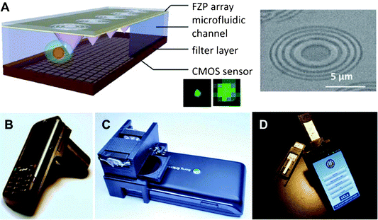 | ||
| Fig. 4 (A) An example application of a Fresnel Zone Plate (FZP) and a microscope image of an actual plate. Improved fluorescent imaging resolution can be achieved in the setup incorporating FZP. (B) An image of the cell phone attachment for holographic-based microscopy. (C) An image of the cell phone attachment for quantum dot-based fluorescence detection in order to determine the concentration of a particle of interest within a sample. (D) An image of a cell phone attachment for reading of commercially available rapid-diagnostic-tests. Images reproduced from ref. 33, 37, 38, 39. | ||
In order to obtain micro-scale (and higher) image resolution, optofluidic imaging devices rely on object scanning, in which constituent parts of a sample object are each imaged independently, and the multiple images are then composited together to form a finalized image of the object. The sample finalized-image acquisition rates of the OFM and the tomographic microscope are comprised of two parts: the rate at which the constituent images are obtained, and the rate at which the constituent images are composited. The devices can of course be used to image single samples, such that the image acquisition rate is not of particular concern. However, the functionality of the devices is improved if they can rapidly image multiple samples, rather than just one (after all, more data of a certain quality is better than less data of the same quality).
One way to improve the image acquisition rate is to increase the rate at which constituent images are obtained. This means either speeding up the sample's transit through the imaging area, or expanding the imaging area and sending multiple samples through at a time. This second approach, where the field of view is expanded so that a single image capture contains multiple samples, has been demonstrated in ref. 35 and 36. We expect future optofluidic imaging devices to continue expanding the device field-of-view in order to increase the rate at which constituent images of a sample are obtained.
A second way to improve the image acquisition rate is to increase the rate at which constituent images are composited to form a finalized image. This will be accomplished through optimizing image processing algorithms. We expect processing algorithms to improve as research groups continue to expand device image gathering capabilities. Some lab groups have already begun the algorithm improvement process.
As pointed out in sections 1 and 2, optofluidic elements that manipulate light in the device plane have proven useful for many on-chip processes (e.g., flow cytometry), but have yet to overcome deficiencies that preclude their use in imaging applications. The primary motivation for imaging systems where light moves in the device plane—as opposed to the out-of-plane direction—is to facilitate imaging device miniaturization (in-plane imaging devices are effectively two-dimensional, whereas out-of-plane imaging devices consume space in the vertical direction as well). A secondary motivation is to facilitate integration with demonstrated in-plane processes, such as flow cytometry or mass spectroscopy. The authors acknowledge these two motivations for in-plane optofluidic imaging systems, but expect most near-term research to be in out-of-plane imaging, as this is where the intriguing research successes have happened.
4.2. Innovations for functional applications
With all of the advances achieved in optofluidic imaging over the last decade, emphasis in the research community has recently shifted to integrating these capabilities—which to date have been primarily demonstrated in laboratories—into fully functional optofluidic imaging devices and systems for real-world application.Recent work by the Ozcan group has led the effort to combine optofluidic devices with standard cell phones, with the intent of creating ultra-portable, ultra-cheap technologies for point-of-care diagnostics and data reporting. One such device uses a simple cell phone attachment (Fig. 4B), consisting of an LED illumination source powered by a battery and filtered through an aperture, to project holograms of a sample onto the cell phone's CMOS image sensor.37 The holograms are then compressed and sent over the network to a computer for holographic reconstruction, and the final processed images are sent back to be viewed on the cell phone.
Another device permits loading of a liquid sample into glass capillaries that have been antibody-functionalized to capture a sample particle of interest. The particles of interest are then tagged with quantum dots and the glass capillaries are illuminated with LEDs.38 The resulting fluorescence emission from the quantum dots is imaged by the cell phone's CMOS sensor, and the concentration of the particle of interest within the sample is derived. The complete device attaches to the back of a standard cell phone, as shown in Fig. 4C.
As a final example of an optofluidic device that pairs with a cell phone, Fig. 4D shows a comprehensive rapid-diagnostic-test (RDT) reader platform that can work with various commercially available immune-chromatographic assays and similar tests to sense the presence of a target analyte in a sample.39 The reader uses three LED arrays to illuminate a RDT, which is imaged by the cell phone's CMOS sensor. An application was also written for the cell phone; this application guides use of the RDT reader, records all resulting data to phone memory and uploads the data to a database/server.
The work by the Ozcan group alone demonstrates the viability of optofluidic imaging platforms for point-of-care medical diagnostics. It also demonstrates the increasingly comprehensive approaches taken to developing optofluidic imaging systems. These systems are more than proof-of-concept devices, they are carefully devised prototypes with comprehensive functionality, accounting for everything from physical size to user interaction to manufacturing cost to software pairing to data compression. We expect this trend of comprehensive engineering within optofluidic imaging research to grow more and more pervasive. The introductory phase of optofluidic imaging research is closing. Now it is time for researchers to show what fully functionalized optofluidic imaging systems can do in the real world.
Acknowledgements
This research was supported by National Institutes of Health (NIH) Director's New Innovator Award (1DP2OD007209-01).References
- F. B. Myers and L. P. Lee, Lab Chip, 2008, 8, 2015–2031 RSC.
- A. W. Martinez, S. T. Phillips, G. M. Whitesides and E. Carrilho, Anal. Chem., 2010, 82, 3–10 CrossRef CAS.
- X. Mao and T. J. Huang, Lab Chip, 2012, 12, 1412–1416 RSC.
- G. Whitesides, Nature, 2006, 442, 368–373 CrossRef CAS.
- A. Arora, G. Simone, G. Salieb-Beugelaar, J. T. Kim and A. Manz, Anal. Chem., 2010, 82, 4830–4847 CrossRef CAS.
- P. Neuzil, S. Giselbrecht, K. Länge, T. J. Huang and A. Manz, Nat. Rev. Drug Discovery, 2012, 11, 620–632 CrossRef.
- V. R. Horowitz, D. D. Awschalom and S. Pennathur, Lab Chip, 2008, 8, 1856–1863 RSC.
- C. Monat, P. Domachuk and B. J. Eggleton, Nat. Photonics, 2007, 1, 106–114 CrossRef CAS.
- N.-T. Nguyen, Biomicrofluidics, 2010, 4, 031501 CrossRef.
- X. Mao, Z. I. Stratton, A. A. Nawaz, S.-C. S. Lin and T. J. Huang, Biomicrofluidics, 2010, 4, 43007 CrossRef.
- X. Mao, J. R. Waldeisen, B. K. Juluri and T. J. Huang, Lab Chip, 2007, 7, 1303–1308 RSC.
- P. Fei, Z. He, C. Zheng, T. Chen, Y. Men and Y. Huang, Lab Chip, 2011, 11, 2835–2841 RSC.
- H. Huang, X. Mao, S.-C. S. Lin, B. Kiraly, Y. Huang and T. J. Huang, Lab Chip, 2010, 10, 2387–2393 RSC.
- S. K. Y. Tang, Z. Li, A. R. Abate, J. J. Agresti, D. A. Weitz, D. Psaltis and G. M. Whitesides, Lab Chip, 2009, 9, 2767–2771 RSC.
- H. Schmidt and A. R. Hawkins, Nat. Photonics, 2011, 5, 598–604 CrossRef CAS.
- Z. Li, Z. Zhang, A. Scherer and D. Psaltis, Opt. Express, 2006, 14, 10494 CrossRef CAS.
- X. Mao, S.-C. S. Lin, C. Dong and T. J. Huang, Lab Chip, 2009, 9, 1583–1589 RSC.
- X. Mao, A. A. Nawaz, S.-C. S. Lin, M. I. Lapsley, Y. Zhao, J. P. McCoy, W. S. El-Deiry and T. J. Huang, Biomicrofluidics, 2012, 6, 24113–241139 CrossRef.
- M. I. Lapsley, I.-K. Chiang, Y. B. Zheng, X. Ding, X. Mao and T. J. Huang, Lab Chip, 2011, 11, 1795–1800 RSC.
- W. Yang, D. B. Conkey, B. Wu, D. Yin, A. R. Hawkins and H. Schmidt, Nat. Photonics, 2007, 1, 331–335 CrossRef CAS.
- S. K. Y. Tang, C. A. Stan and G. M. Whitesides, Lab Chip, 2008, 8, 395–401 RSC.
- X. Mao, S.-C. S. Lin, M. I. Lapsley, J. Shi, B. K. Juluri and T. J. Huang, Lab Chip, 2009, 9, 2050–2058 RSC.
- D. V. Vezenov, B. T. Mayers, R. S. Conroy, G. M. Whitesides, P. T. Snee, Y. Chan, D. G. Nocera and M. G. Bawendi, J. Am. Chem. Soc., 2005, 127, 8952–8953 CrossRef CAS.
- S. Xiong, A. Q. Liu, L. K. Chin and Y. Yang, Lab Chip, 2011, 11, 1864–1869 RSC.
- W. Song and D. Psaltis, Lab Chip, 2011, 11, 2397–2402 RSC.
- X. Cui, L. M. Lee, X. Heng, W. Zhong, P. W. Sternberg, D. Psaltis and C. Yang, Proc. Natl. Acad. Sci. U. S. A., 2008, 105, 10670–10675 CrossRef CAS.
- X. Heng, D. Erickson, L. R. Baugh, Z. Yaqoob, P. W. Sternberg, D. Psaltis and C. Yang, Lab Chip, 2006, 6, 1274–1276 RSC.
- S. O. Isikman, W. Bishara, U. Sikora, O. Yaglidere, J. Yeah and A. Ozcan, Lab Chip, 2011, 11, 2222–2230 RSC.
- D. Lange, C. W. Storment, C. A. Conley and G. T. A. Kovacs, Sens. Actuators, B, 2005, 107, 904–914 CrossRef.
- S. Pang, X. Cui, J. DeModena, Y. M. Wang, P. Sternberg and C. Yang, Lab Chip, 2010, 10, 411–414 RSC.
- S. O. Isikman, W. Bishara, S. Mavandadi, F. W. Yu, S. Feng, R. Lau and A. Ozcan, Proc. Natl. Acad. Sci. U. S. A., 2011, 108, 7296–7301 CrossRef CAS.
- B. Huang, W. Wang, M. Bates and X. Zhuang, Science, 2008, 319, 810–813 CrossRef CAS.
- S. Pang, C. Han, L. M. Lee and C. Yang, Lab Chip, 2011, 11, 3698–3702 RSC.
- E. Schonbrun, A. R. Abate, P. E. Steinvurzel, D. A. Weitz and K. B. Crozier, Lab Chip, 2010, 10, 852–856 RSC.
- A. F. Coskun, T.-W. Su and A. Ozcan, Lab Chip, 2010, 10, 824–827 RSC.
- X. Zhang, I. Khimji, U. A. Gurkan, H. Safaee, P. N. Catalano, H. O. Keles, E. Kayaalp and U. Demirci, Lab Chip, 2011, 11, 2535–2540 RSC.
- D. Tseng, O. Mudanyali, C. Oztoprak, S. O. Isikman, I. Sencan, O. Yaglidere and A. Ozcan, Lab Chip, 2010, 10, 1787–1792 RSC.
- H. Zhu, U. Sikora and A. Ozcan, Analyst, 2012, 137, 2541–2544 RSC.
- O. Mudanyali, S. Dimitrov, U. Sikora, S. Padmanabhan, I. Navruz and A. Ozcan, Lab Chip, 2012, 12, 2678–2686 RSC.
| This journal is © The Royal Society of Chemistry 2013 |