Analysis of molecular monolayers adsorbed on metal surfaces by glow discharge optical emission spectrometry
Igor S.
Molchan
*a,
George E.
Thompson
a,
Peter
Skeldon
a,
Antonino
Licciardello
b,
Nunzio
Tuccitto
b and
Agnes
Tempez
c
aCorrosion and Protection Centre, School of Materials, The University of Manchester, The Mill, Sackville St., Manchester, M13 9PL, UK. E-mail: igor.molchan@manchester.ac.uk
bDipartimento di Scienze Chimiche, Universita' di Catania, Viale A. Doria 6, 95125, Catania, Italy
cHORIBA Jobin Yvon, 16/18 rue du Canal, 91160, Longjumeau, France
First published on 30th October 2012
Abstract
The pioneering study of Shimizu et al. (J. Anal. At. Spectrom., 2004, 19, 692) on the examination of adsorbed organic molecules on a copper substrate by radio frequency glow discharge optical emission spectrometry (rf-GDOES) displayed the potential of GDOES for determination of the orientations of molecular monolayers. Here, the study has been extended to the examination of thiourea adsorbed on silver, gold and copper surfaces and metal-centred molecular wires (MCMWs) of 4–6 nm length, with cobalt atoms in the middle of the chain adsorbed on a gold surface. According to established data, these molecules are adsorbed onto a metal surface through a sulphur atom. Depth profiling of thiourea adsorbed on the copper surface confirmed the results of Shimizu et al., with a nitrogen peak followed by a sulphur peak in the depth profile revealed with sputtering time. However, in the case of silver and gold substrates, the positions of the sulphur and nitrogen peaks in the depth profiles were not as predicted from the orientation of the thiourea molecule, i.e. the nitrogen peak followed the sulphur peak with sputtering time or the peaks overlapped. In the depth profiles of the adsorbed MCMWs, the sulphur peak appeared prior to the cobalt peak with sputtering time. Further, the time required for sputtering of thiourea and the wires are comparable, whereas the lengths of thiourea and the wire molecules differ by more than one order of magnitude. Thus, in this case, no correlation between the orientation of the molecules and the peak sequence in the depth profiles has been observed.
Introduction
GDOES is now a widely accepted technique for qualitative/quantitative elemental depth profiling of solids. The technique offers high accuracy, typically a few nanometres, achievable with a relatively short duration of analysis; analyses of oxide films of several hundred nanometres thickness last from seconds to several tens of seconds depending on the type of material and plasma parameters. For example, GDOES examination of an anodic film of 360 nm thickness, formed on 99.99% purity aluminium, requires about 20 s and enables ready observation of 4 nm thick layers containing chromium, chlorine and phosphorus impurities located within an anodic film and a 2 nm thick copper-enriched layer located immediately beneath the anodic alumina/aluminium interface.2 GDOES was demonstrated to be a powerful tool in the study of transport processes during formation of anodic films on aluminium and other valve metals and alloys.3,4 Further, the technique was successfully utilised for analysis of elemental distributions in thin layers, a few nanometres thickness, on aluminium and steel covered by air-formed oxide films.5,6 Shimizu et al.1 analysed thiourea and benzotriazole molecules adsorbed on mirror-polished copper surfaces by GDOES. It is firmly established that the thiourea molecule is adsorbed on the copper surface through the sulphur atom and it is aligned nearly perpendicular to the copper surface.7 Conversely, benzotriazole is adsorbed on the copper surface with its molecular plane parallel to the surface.8 The appearance of a narrow nitrogen peak prior to a sulphur peak during GDOES depth profiling of thiourea adsorbed on the copper surface was revealed. The finding was attributed to consecutive removal of the atoms of the molecule aligned perpendicular to the metal surface. In contrast, during depth profiling of the benzotriazole molecule, carbon, nitrogen and hydrogen peaks appeared at nearly the same locations on the time axis. The results were associated with atomic-scale resolution achieved by GDOES and, thus, the potential of GDOES for determining the orientation of molecular monolayers adsorbed on metal surfaces. However, a study published recently by Klemm et al.9 concerning GDOES examination of a benzotriazole or benzothiazole monolayer adsorbed on a copper surface did not reveal any correlation between the orientation of the molecule and the peak sequence in the depth profiles. The finding was attributed to processes in the plasma after breaking of the molecule into single atoms or fragments under bombardment by Ar+ ions.Similar to the adsorption on copper, thiourea molecules are also capable of adsorbing on other metals e.g. silver or gold, through the sulphur end, with perpendicular or tilted orientations of the molecule with respect to the metal surface.7,10–12 Recently, we carried out GDOES depth profiling of thiourea monolayers adsorbed on copper, silver and gold surfaces and MCMWs, adsorbed on gold. The MCMWs were similar to those reported by Tuccitto et al.13 Excellent reproducibility with the results obtained by Shimizu et al. was achieved in the case of thiourea adsorbed on copper. However, in the case of silver and gold substrates, no correlation between the expected orientation of the molecules and the peak sequence in depth profiles was revealed. The results of the study are discussed here.
Experimental
Bulk copper and silver coupons (99.99% purity in both cases) were used in the present study. The coupons, of dimensions of 30 × 30 mm, were mechanically polished using, consecutively, P1200 emery paper, 3 and 1 μm diamond pastes, and, finally, 0.3 and 0.05 μm alumina powders. As a result, surfaces with mirror-like appearance were generated. After polishing, the coupons were rinsed thoroughly in acetone and ethanol followed by washing in deionised water in an ultrasonic bath to remove residuals of the polishing paste and other related products. Polishing and rinsing were carried out immediately before immersion in thiourea to minimise growth of oxide films on the substrate surface. Additionally, copper was deposited by magnetron sputtering onto the polished surface of a monocrystalline silicon wafer. Sputter deposition of copper was performed using a 99.99% purity copper target for 30 min at a constant current of 200 mA, with a residual gas pressure of 3 × 10⁻⁷ mbar and a total pressure of 5 × 10⁻³ mbar of purified argon. Examination of the mechanically polished copper surface by atomic force microscopy revealed a roughness of 2.5 nm over the scanned area of 2 × 2 μm. The roughness of the copper surface deposited by magnetron sputtering was about 3 nm. The polished silver exhibited a roughness of about 4 nm. Gold-coated, silicon wafers were purchased from Sigma-Aldrich. The purity and thickness of the gold layer were 99.999% and 100 nm respectively. An 0.01 M aqueous thiourea solution was used. Immediately prior to GDOES examination, the substrates were immersed in the solution for 2 min at room temperature, followed by drying in a cold air stream.MCMWs were grown on a platform comprised of a self-assembled monolayer (SAM) on gold of mixed-component SAMs of 4′-(4-mercaptophenyl)-2-2′:6′2′′-terpyridine (MPTP) and mercapto benzene (MB) with 1![[thin space (1/6-em)]](https://www.rsc.org/images/entities/char_2009.gif) :1 molar ratio. Preparation of the MPTP/MB platform has been described elsewhere.14 MCMWs were assembled on this gold-supported ‘platform’ SAM by a stepwise procedure involving sequential coordination reactions with a metal centre and a symmetric ligand with two terpyridine units symmetrically bound to a phenyl ring, 1,4-di(2;2′;6′,2′-terpyridine-4′-yl)benzene (TPT).13 The silicon wafer supported gold layer was (1) immersed for 1 min in a solution of Co(II) salt (0.05 M in water–ethanol, 1:1), and sequentially rinsed with water, ethanol and chloroform, (2) immersed for 15 min in TPT solution and rinsed with warm chloroform (∼40 °C), ethanol and water. Stages (1) and (2) were repeated iteratively, with iteration representing a ‘coordination step’ that adds one metal–ligand unit to the MCMW, until the desired length was reached. The MCMWs were analysed by GDOES after approximately 4–5 days from preparation.
:1 molar ratio. Preparation of the MPTP/MB platform has been described elsewhere.14 MCMWs were assembled on this gold-supported ‘platform’ SAM by a stepwise procedure involving sequential coordination reactions with a metal centre and a symmetric ligand with two terpyridine units symmetrically bound to a phenyl ring, 1,4-di(2;2′;6′,2′-terpyridine-4′-yl)benzene (TPT).13 The silicon wafer supported gold layer was (1) immersed for 1 min in a solution of Co(II) salt (0.05 M in water–ethanol, 1:1), and sequentially rinsed with water, ethanol and chloroform, (2) immersed for 15 min in TPT solution and rinsed with warm chloroform (∼40 °C), ethanol and water. Stages (1) and (2) were repeated iteratively, with iteration representing a ‘coordination step’ that adds one metal–ligand unit to the MCMW, until the desired length was reached. The MCMWs were analysed by GDOES after approximately 4–5 days from preparation.
A GD-Profiler 2 (Horiba Jobin Yvon), operating in the radio frequency mode at 13.56 MHz, was employed for examination of the substrates with adsorbed monolayers. A 4 mm diameter copper anode and argon gas were used. The emission responses from the excited sputtered elements were detected with a polychromator of a focal length of 500 mm with 30 optical windows. Elemental depth profiling was carried out in a real power mode at 700 Pa and 35 W, with a data acquisition time of 0.001 s. The samples with a magnetron sputtered copper layer were examined at powers of 10, 15 and 35 W. Immediately prior to depth profiling, pre-sputtering of a sacrificial silicon wafer was undertaken at the power and pressure used for depth profiling to provide a clean GD source.15 This procedure resulted in the removal of contaminants from the inner anode walls by the relatively high-energy plasma and covering of the anode walls with a thin silicon layer. The thin deposited silicon layer prevented any underlying contaminant layer from sputtering and stabilised the plasma at the commencement of depth profiling. Additionally, a long flush time of 300 s was utilised before commencement of depth profiling to further clean the plasma source. The emission lines used were 156.14 nm for carbon, 345.35 nm for cobalt, 324.75 nm for copper, 242.79 nm for gold, 121.56 nm for hydrogen, 149.26 nm for nitrogen, 130.21 nm for oxygen, 180.73 nm for sulphur and 288.15 nm for silicon. A monochromator, adjusted for a line at 338.28 nm, was employed to acquire the response from silver.
Results and discussion
The depth profile of thiourea adsorbed on the copper coupon reveals excellent reproducibility with the results reported by Shimizu et al.1 and then repeated by Klemm et al.9 (Fig. 1(a)). A nitrogen peak is followed by a sulphur peak with an increase of sputtering time. The intensities of the nitrogen and sulphur peaks in the depth profile of the copper substrate that had not been immersed in thiourea solution are significantly weaker, with no evidence of separation in time (Fig. 1(b)). Thus, the nitrogen and sulphur peaks of Fig. 1(a) are associated with thiourea. The presence of a weak sulphur peak in the depth profile of the copper substrate may originate from atmospheric sulphur contamination. Secondly, the sulphur signal may interfere with the carbon signal; the weak sulphur peak overlaps with the carbon shoulder in Fig. 1(b). The similar weak sulphur peaks at the commencement of sputtering were observed in the elemental depth profiles of mechanically polished silver, monocrystalline silicon, gold-coated monocrystalline silicon and the copper layer deposited on monocrystalline silicon by magnetron sputtering. It is difficult to interpret the carbon and hydrogen profiles of Fig. 1(a) because they can originate from both thiourea and hydrocarbon contaminants present on the substrate and in the GD source. The carbon signal of Fig. 1(a) exhibits a narrow surge at the commencement of sputtering followed by a much wider peak. The first surge appears due to instability of the plasma at the commencement of sputtering and the second peak is associated with thiourea and hydrocarbon contaminants. In Fig. 1(b), the carbon signal shows an intense carbon surge due to plasma instability followed by a shoulder originating from contaminants. The increased intensity of the second carbon peak in Fig. 1(a) compared with the intensity of the carbon shoulder in Fig. 1(b) may be associated with the contribution of thiourea. The inset of Fig. 1(b) displays the carbon and copper signals and the parameter Fi (total light in the polychromator) plotted on the same intensity scale as the depth profile of Fig. 1(b). A surge in the Fi signal is evident in the first 0.002 s of sputtering, indicating plasma instability. Carbon and copper signals follow the Fi behaviour in the first 0.002 s of sputtering. The carbon surge intensity reached up to 16000 a.u. on the same a.u. scale in other depth profiling and is most likely related to transition processes in the instrument electronics at the start of glow discharge. The hydrogen behaviour is similar in the depth profiles of Fig. 1(a) and (b); the hydrogen signals exhibit a peak with a tail centred at around 0.004–0.005 s of sputtering. The hydrogen signal may be associated with hydrocarbon contaminants. Probably the contribution of the hydrogen atoms of thiourea to the hydrogen signal is insignificant. The intensity of a hydrogen peak of the copper substrate is slightly increased compared with that of copper with adsorbed thiourea and may be associated with variation of the amount of hydrocarbon contaminants on the substrate and in the GD source. Interestingly, a similar sequence of nitrogen and sulphur peaks was revealed when the copper was immersed in thiourea solution and examined on the fourth day after preparation. Further, the sequence of peaks remained the same when copper was immersed in a solution with a thiourea concentration up to 0.5 M.
 | ||
| Fig. 1 GDOES elemental depth profiles of (a) mechanically polished copper with an adsorbed thiourea layer and (b) mechanically polished copper. The inset of (b) shows the behaviour of C, Cu and Fi signals at the commencement of sputtering. | ||
Examination of thiourea adsorbed on the copper layer formed by magnetron sputtering on monocrystalline silicon revealed that the sequence of nitrogen and sulphur peaks does not change when the power is reduced from 35 to 10 W (Fig. 2). The carbon peaks exhibit surges at the commencement of sputtering followed by shoulders related to thiourea and contaminants. The hydrogen signal behaviour is similar to that of Fig. 1. Insets display the depth profiles plotted on the extended time scale to show the time necessary to sputter completely the copper layer. The full width at half maximum (FWHM) of the sulphur and nitrogen peaks and the time necessary for complete sputtering of the copper layer, tCu, at powers ranging from 35 to 10 W are presented in Table 1. In GD techniques, the sputtering rate qM is nearly proportional to the applied power Pg:16
| qM = k(Pg − P0), |
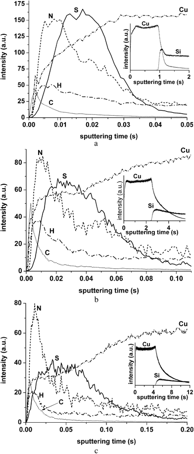 | ||
| Fig. 2 GDOES elemental depth profiles of thiourea adsorbed on a copper layer deposited by magnetron sputtering on monocrystalline silicon recorded at various powers of the GD source: (a) 35 W, (b) 15 W, and (c) 10 W. Insets: the same profiles showing the time necessary to reach the silicon substrate. | ||
| Power | NFWHM, s | SFWHM, s | t Cu, s |
|---|---|---|---|
| 35 W | 0.019 | 0.019 | 1.0 |
| 15 W | 0.020 | 0.044 | 2.5 |
| 10 W | 0.021 | 0.076 | 4.6 |
Fig. 3 displays the depth profiles of thiourea adsorbed on a silver coupon, recorded at two different locations over the sample surface, with the presence of sulphur and nitrogen peaks revealed. The intensities of sulphur and nitrogen peaks in the depth profile of silver that had not been immersed in thiourea solution are approximately 20 and 3 times less respectively, which is indicative of the presence of adsorbed thiourea. A different order of sulphur and nitrogen peaks is evident in the depth profiles. The sulphur peak is followed by the nitrogen peak with sputtering time (Fig. 3(a)) or the peaks overlap (Fig. 3(b)). Insets of Fig. 3(a) and (b) show that the sulphur signal has a similar shoulder to the carbon signal that has been discussed previously. The reduced peak to tail intensity ratios in the nitrogen signals compared with that of Fig. 1(a) may be due to less thiourea molecules adsorbed on silver. The different sequence of the nitrogen and sulphur peaks needs further investigation. The reduced reproducibility may be related, for instance, due to the presence of different orientations of thiourea molecules over the macroscopic surface of the silver substrate or slightly increased roughness compared with that of the copper substrate. The FWHM of the sulphur and nitrogen peaks obtained at 35 W varied from 0.004 to 0.008 s and from 0.007 to 0.012 s respectively. Reduction of power to 10 W resulted in an increase of the FWHM to 0.012–0.017 s and 0.011–0.018 s for sulphur and nitrogen peaks respectively. Thus, similar to copper, increased widening of the sulphur peak compared with that of the nitrogen peak was observed with reduction of power.
 | ||
| Fig. 3 GDOES elemental depth profiles of mechanically polished silver immersed in thiourea solution recorded at two different locations over the macroscopic silver surface revealing (a) sulphur peak followed by a nitrogen peak and (b) overlapping sulphur and nitrogen peaks. Insets show the shape of the sulphur and carbon signals on an extended sputtering time scale. | ||
Depth profiling of thiourea adsorbed on a gold surface reveals that the nitrogen and sulphur peaks overlap (Fig. 4). The intensities of the nitrogen and sulphur peaks in the depth profile of the as-received gold-coated surface are significantly less, confirming the presence of thiourea on the gold surface.
 | ||
| Fig. 4 GDOES elemental depth profile of thiourea adsorbed on gold-coated monocrystalline silicon. | ||
Further, examination of MCMWs assembled on a gold surface, consisting of much longer chains, did not reveal an order of peaks that can be immediately correlated with the atom sequence in the wire (Fig. 5). The MCMW is bound to the gold surface through sulphur, while cobalt centres, coordinated by nitrogen atoms, are located inside the chain and separated from sulphur by an 0.7 nm long organic part and separated each by a ∼1 nm long TPT unit. For this reason, cobalt, nitrogen and sulphur were selected as probe elements to identify the molecule. The sulphur peak appears prior to the cobalt peak with sputtering time, with the sulphur and nitrogen peaks overlapping, presenting no evidence of a step-by-step elemental removal of the molecule. Further, the time necessary for sputtering of MCMW is less than 0.02 s, which is comparable with that necessary for sputtering thiourea adsorbed on a copper, silver or gold substrate. On the other hand, the length of the wires is 4–6 nm, whereas the lengths of the C–S and C–N bonds in the thiourea molecule are approximately 0.17 and 0.13 nm respectively, with an S–C–N angle of 122 degrees.19
 | ||
| Fig. 5 GDOES elemental depth profile of cobalt-centred molecular wires adsorbed on the gold-coated monocrystalline silicon substrate. | ||
Conclusions
The results of GDOES depth profiling of thiourea adsorbed on copper are in good agreement with those reported previously, i.e. the depth profiles reveal a nitrogen peak followed by a sulphur peak with an increase of sputtering time. Conversely, GDOES analysis of thiourea on a silver or gold surface does not reveal the same sequence of nitrogen and sulphur peaks. It should be noticed that further studies are required to confirm the orientation of the thiourea molecules on gold and silver surfaces. However, depth profile of MCMWs that are adsorbed on the gold surface through sulphur and are tilted at an angle of 40 degrees to the surface normal shows the “wrong” sequence of peaks, i.e. the sulphur peak is followed by the cobalt peak with sputtering time. Thus, it is considered that desorption of intact molecules or molecular clusters, including those bound with atoms of the substrate, takes place during sputtering, and these fragments do not leave the metal surface in an ordered manner. Further experiments on GDOES examination of other molecular layers adsorbed on metal surfaces are required to clarify the mechanisms involved in their behaviour in the GD plasma.References
- K. Shimizu, R. Payling, H. Habazaki, P. Skeldon and G. E. Thompson, J. Anal. At. Spectrom., 2004, 19, 692–695 RSC.
- I. S. Molchan, G. E. Thompson, P. Skeldon, N. Trigoulet, A. Tempez and P. Chapon, Trans. Inst. Met. Finish., 2010, 88, 154–157 CrossRef CAS.
- K. Shimizu, G. M. Brown, H. Habazaki, K. Kobayashi, P. Skeldon, G. E. Thompson and G. C. Wood, Corros. Sci., 1999, 41, 1971–1976 CrossRef CAS.
- H. Habazaki, K. Fushimi, K. Shimizu, P. Skeldon and G. E. Thompson, Electrochem. Commun., 2007, 9, 1222–1227 CrossRef CAS.
- K. Shimizu, H. Habazaki, P. Skeldon, G. E. Thompson and G. C. Wood, Surf. Interface Anal., 1999, 27, 998–1002 CrossRef CAS.
- K. Shimizu, H. Habazaki, P. Skeldon, G. E. Thompson and G. C. Wood, Surf. Interface Anal., 2000, 29, 743–746 CrossRef CAS.
- B. H. Loo, Chem. Phys. Lett., 1982, 89, 346–350 CrossRef CAS.
- C. Törnkvist, D. Thierry, J. Bergman, B. Liedberg and C. Leygraf, J. Electrochem. Soc., 1989, 136, 58–64 CrossRef.
- D. Klemm, V. Hoffmann, K. Wetzig and J. Eckert, Anal. Bioanal. Chem., 2009, 395, 1893–1900 CrossRef CAS.
- M. Fleischmann, I. R. Hill and G. Sundholm, J. Electroanal. Chem., 1983, 157, 359–368 CAS.
- H. Wroblowa and M. Green, Electrochim. Acta, 1963, 8, 679–692 CrossRef CAS.
- R. Holze and S. Schomaker, Electrochim. Acta, 1990, 35, 613–620 CrossRef CAS.
- N. Tuccitto, V. Ferri, M. Cavazzini, S. Quici, G. Zhavnerko, A. Licciardello and M. A. Rampi, Nat. Mater., 2009, 8, 41–46 CrossRef CAS.
- A. Auditore, N. Tuccitto, G. Marzanni, S. Quici, F. Puntoriero, S. Campagna and A. Licciardello, Chem. Commun., 2003, 2494–2495 RSC.
- I. S. Molchan, G. E. Thompson, P. Skeldon, N. Trigoulet, P. Chapon, A. Tempez, J. Malherbe, L. Lobo Revilla, N. Bordel, Ph. Belenguer, T. Nelis, A. Zahri, L. Therese, Ph. Guillot, M. Ganciu, J. Michler and M. Hohl, J. Anal. At. Spectrom., 2009, 24, 734–741 RSC.
- R. Payling, M. Aeberhard, J. Michler, C. Authier, P. Chapon, T. Nelis and L. Pitchford, Surf. Interface Anal., 2003, 35, 334–339 CrossRef CAS.
- N. Tuccitto, V. Torrisi, I. Delfanti and A. Licciardello, Appl. Surf. Sci., 2008, 255, 874–876 CrossRef CAS.
- S. Canulescu, I. S. Molchan, A. Tempez, C. Tauziede, J. A. Whitby, G. E. Thompson, P. Chapon and J. Michler, Anal. Bioanal. Chem., 2010, 396, 2871–2879 CrossRef CAS.
- N. R. Kunchur and M. R. Truter, J. Chem. Soc., 1958, 2551–2557 RSC.
| This journal is © The Royal Society of Chemistry 2013 |