Graphene/semiconductor heterojunction solar cells with modulated antireflection and graphene work function†
Yuxuan
Lin‡
a,
Xinming
Li‡
b,
Dan
Xie
*a,
Tingting
Feng
a,
Yu
Chen
a,
Rui
Song
a,
He
Tian
a,
Tianling
Ren
*a,
Minlin
Zhong
b,
Kunlin
Wang
b and
Hongwei
Zhu
*bc
aTsinghua National Laboratory for Information Science and Technology (TNList), Institute of Microelectronics, Tsinghua University, Beijing 100084, P. R. China. E-mail: xiedan@tsinghua.edu.cn; rentl@tsinghua.edu.cn
bKey Laboratory for Advanced Manufacturing by Material Processing Technology, Ministry of Education and Department of Mechanical Engineering, Tsinghua University, Beijing 100084, P. R. China. E-mail: hongweizhu@tsinghua.edu.cn; Fax: +86 10 62773637; Tel: +86 10 62781065
cCenter for Nano and Micro Mechanics (CNMM), Tsinghua University, Beijing 100084, P. R. China
First published on 6th November 2012
Abstract
Theoretical and experimental studies have been performed to simulate and optimize graphene/semiconductor heterojunction solar cells. By controlling graphene layer number, tuning graphene work function and adding an antireflection film, a maximal theoretical conversion efficiency of ∼9.2% could be achieved. Following the theoretical optimization proposal, the Schottky junction solar cells with modified graphene films and silicon pillar arrays were fabricated and were found to give a conversion efficiency of up to 7.7%.
Broader contextGraphene-based photovoltaic devices have attracted great interest since the recent implementation of graphene/semiconductor heterojunction solar cells, due to the fascinating electronic and optical characteristics of graphene, revealing its promising potential in use as transparent electrodes, hole collectors and junction layers. A theoretical approach is presented to simulate and optimize the graphene/semiconductor Schottky junction solar cells. Possible optimization methods are proposed to improve the cell performance, including antireflection film addition, graphene work function and layer number modulation. Simulation results demonstrate that a maximal conversion efficiency of ∼9.2% can be achieved. To verify, Schottky junction solar cells based on acid-modified graphene films and silicon pillar arrays are fabricated, delivering enhanced cell performance with efficiencies of up to 7.7%. |
1 Introduction
Graphene, the 2-dimensional hexagonal crystal of carbon,1–3 has stimulated tremendous research interest primarily due to its excellent electronic, mechanical and optical characteristics, such as ultrahigh mobility,1,4 outstanding flexibility and stability,5,6 excellent thermal conductivity,7–9 and especially, its high transmittance within the visible-infrared region.10 Early research works mainly focused on graphene-based field effect transistors.11–15 Despite extensive research, the much anticipated shift from silicon to graphene in microelectronic industry seriously fell short due to the low on–off ratios and the difficulties in preparing high quality graphene films or nanoribbons. On the other hand, the applications of graphene have spread into many other fields, such as nano-mechanical systems (NEMS),16 non-volatile memory,17,18 optoelectronics,19–22 interconnections,23,24 thermal management25 and bioelectronics.26–28 Among these applications, graphene-based solar cells are the most reputable because of their remarkable performances as transparent electrodes and active layers for photoelectric devices,29,30 which make them promising solutions for fast-response and energy efficient applications.Graphene-based heterojunction solar cells were first studied by Zhu et al.,22 where graphene served as a transparent electrode and introduced a built-in electric field near the interface between the graphene and n-type silicon to help collect photo-generated carriers (see Fig. 1). Such a heterojunction photovoltaic effect achieved a maximal conversion efficiency of ∼4.35%.31 Lim et al.32 noted that the open-circuit voltage of a similar solar device varied in correlation with the graphene layer number, whereas the efficiency remained quite low. More studies are still necessary to realize the full potential of this new type of photovoltaic device.
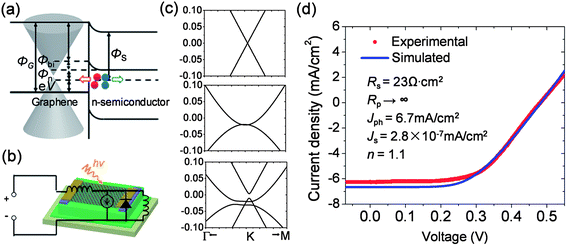 | ||
| Fig. 1 A graphene/semiconductor photovoltaic device. (a) Band diagram of a forward biased (with voltage V) Schottky junction. ΦS and ΦG are the work function of semiconductor and graphene, respectively. Φbi is the built-in potential, Φn is the energy difference between the semiconductor's conductance band and Fermi level, and χ is the electron affinity of the semiconductor. The grey cones indicate the linear dispersion of graphene near the Dirac point. The red and blue spheres represent the electrons and holes generated by the incident light and separated by the built-in potential. (b) An equivalent circuit model. The ideal device is treated as an ideal diode in parallel with a current source. Parasite resistances (series resistance Rs and parallel resistance Rp) are included in the circuit model. (c) Dispersion of electrons in mono- (upper), bi- (middle), and tri-layer (lower) graphene near the Dirac point. K, Γ and M stand for the high symmetry points in the Brillouin zone. The vertical axes indicate the energy of electrons in graphene (eV). (d) Comparison of simulated and experimental J–V curves. | ||
In this paper, a theoretical model is presented to simulate the performance of graphene/semiconductor heterojunction solar cells. Using parameters extracted from experiments, our simulation gives consistent results with tested performance. Based on our theoretical analysis, two practical optimization treatments have been proposed. First, the work function (WF) and layer number of graphene should be carefully adjusted. Recent studies have made it possible to control graphene WF (3.5–5.1 eV) through applying an electric field33 or chemical doping.34–36 With a large WF, the built-in potential is amplified near the junction, which consequently improves the photo-generated carrier collection capacity of the heterojunction. Furthermore, the layer number of graphene should be carefully tuned to ensure the optimal combination of sheet resistance and film transmittance. Second, antireflection (AR) layers should be introduced to mitigate the energy dissipation from the optical reflection. Polished single-crystalline silicon wafers have >35% reflectance for visible light (350–800 nm).37 To overcome this problem, an AR technique has been developed to suppress the reflectance of solar cells. A periodic patterned surface, called a pillar-array (PA) structure, is considered to reduce the reflectance to approximately 0.01% under air mass 1.5 conditions. The theoretical conversion efficiency of our optimized photovoltaic device reaches ∼9.2%. To verify the simulation result, solar cells based on acid-modified graphene films and/or silicon pillar arrays were assembled, tested, and were found to deliver improved efficiencies of up to 7.7%, which is higher than our previously reported experimental values.22,31
2 Experimental
2.1 Theoretical approaches
In the graphene/semiconductor solar cell heterojunction, the interface between graphene and semiconductor plays the central role in energy conversion, and both the front and back metal contacts are deposited to attach outlet terminal wires. When intrinsic p-doped or metallic graphene and n-doped semiconductor with a prominent work function difference are in contact with each other, electrons on the semiconductor side are depleted, which bends the energy band (diagram shown in Fig. 1a and S1†) to form a built-in electric field. This built-in potential splits the excess electrons and holes generated by incident light, hence converting light energy into electric energy. The circuit model and circuit equations are presented in Fig. 1b, and eqn (1) and (2), respectively:| J′ = −Jph + Js(eV′/nVt−1) | (1) |
 | (2) |
The photo-generated current density (Jph) can be calculated by integrating the current density response of monochromic incident light with photon energy ħω (denoted as jph) over the range where the incident photon energy is larger than the semiconductor's forbidden band energy Eg, that is,  . Here jph is obtained through solving continuity equations (see ESI† for detailed deduction). The diode is a Schottky junction, so the reverse saturation current density Js is exponentially dependent of the Schottky barrier height ΦB0 = ΦG − χ, where ΦG and χ are the graphene work function and electron affinity of the semiconductor, respectively. The series resistance Rs consists of (i) the contact resistance between the top electrode and graphene, (ii) the contact resistance between the back electrode and semiconductor, (iii) the bulk resistance of the semiconductor, and most importantly, (iv) the resistance of graphene. The parallel resistance Rp reflects the current leakage of the junction, most probably because of the poor insulation between the top electrode and the substrate or the quantum tunnelling effect in the junction barrier.
Both the optical and electrical behaviours of graphene are formulated in our model. The optical response of graphene is described by the classic electromagnetic field theory, and the imaginary part of the complex dielectric constant used in this model and the optical conductivity are calculated according to the Kubo formula given by Stauber et al.38 The calculated transmittance of graphene is in good agreement with the experimental results.10 The resistance of graphene is calculated by RG = kRsh, where Rsh is the sheet resistance of graphene, and k is a proportionality factor determined by geometric dimensions of devices. Rsh can be calculated by
 | (3) |
To calculate both the optical and electric conductivity, the E–k relation of graphene is needed. Using a tight-binding approach, the 2N-dimensional Hamiltonian of N layer number graphene is obtained. The 2N eigenvalues of the Hamiltonian at different points in k-space extend into 2N energy bands, which are called E–k relation or the energy dispersion. The E–k relations of mono-, bi- and trilayer graphene near the Dirac point are plotted in Fig. 1c (the whole E–k relation plots are given in Fig. S3 in the ESI†). In contrast to monolayer graphene, the E–k relations of bilayer, trilayer and even multilayer graphene are no longer linear, and there are slight band overlaps. The carrier state density as a function of energy, carrier density and optical conductivity can be subsequently obtained.
Our theoretical treatment of the optical response of the air–graphene–semiconductor system is based on the thin-film model.39 The silicon-pillar array AR film, if any, is treated as a plane-stratified dielectric film with various equivalent refraction indices toward the direction of the thickness.37
To better describe the real performance of the devices, several parameters in our theoretical model are extracted from experimental results, including the ideal factor n in eqn (1), and the dimensional proportion factor k in the expression of graphene resistance RG. Fig. 1d and S4 (in the ESI†) compare our simulated J–V curve and the experimental J–V curve from.22 The good agreement between theoretical and experimental results confirms the validity of our model. Detailed model description and related deduction are given in the ESI.†
2.2 Material synthesis, device assembly and characterizations
Graphene synthesis was carried out using a typical methane CVD method in a quartz tube within a thermal furnace. Copper foil was placed in the tube. Before graphene growth, the tube was purified with argon and then heated up to 1000 °C in an argon–hydrogen mixture (200![[thin space (1/6-em)]](https://www.rsc.org/images/entities/char_2009.gif) :5 mL min−1), after which a methane flow was introduced to the quartz tube at a methane–hydrogen–argon ratio of 10:2:200 (mL min−1). After graphene growth, the copper foil was pulled out to the room temperature zone and the furnace was cooled down under a hydrogen–argon atmosphere. The graphene film was detached by etching the copper away with aqueous FeCl3 solution (1 M).
:5 mL min−1), after which a methane flow was introduced to the quartz tube at a methane–hydrogen–argon ratio of 10:2:200 (mL min−1). After graphene growth, the copper foil was pulled out to the room temperature zone and the furnace was cooled down under a hydrogen–argon atmosphere. The graphene film was detached by etching the copper away with aqueous FeCl3 solution (1 M).
Single-crystal n-Si (100) wafers with 300 nm SiO2 were used as the starting material. The SiO2 layer was then patterned to become the isolation layer between Si and the front contact. The front electrodes Ti/Au and back electrodes Ti/Pd/Ag were deposited through e-beam evaporation. After that, the pillar arrays were fabricated through photolithography and reactive ion etching (RIE). Graphene grown by CVD was transferred onto the pillar-array-patterned area. The effective illumination area of the cell was 0.1 cm2, and the exposed Si was patterned to form column pillar arrays that are 1.9 μm in diameter and from 200 nm to 1 μm in depth. HNO3 modification was carried out by exposing the graphene films to HNO3 fumes. The assembled graphene/n-Si solar cells were placed above a vial containing fuming HNO3 (65 wt%). The treatment time was carefully controlled to avoid corrosion of silver and underlying Si. The solar devices were tested with a solar simulator (Newport) under AM 1.5 conditions. The current–voltage data were recorded with a Keithley 2602 SourceMeter.
3 Results and discussion
In our simulation, three factors are found to considerably impact the collecting efficiency of photo-generated excess carriers and need to be improved: (i) the optical reflectance of the pristine graphene–silicon system is about 35%,37 resulting in a notable decrease in cell efficiency; (ii) the parasitic resistances dissipate the converted electric energy; and (iii) the amplitude of the built-in potential near the heterojunction is not large enough to effectively dissociate hole–electron pairs. Both the second and third drawbacks can be reduced through careful modulation of the work function as well as the layer number of graphene. To solve the first problem related to the optical reflection, an AR technique has been developed.3.1 Graphene work function and layer number modulation
The WF of graphene determines both the junction built-in potential and the graphene sheet resistance, as demonstrated in Fig. 2a. Here we assume that the junction between graphene and semiconductor is an ideal Schottky contact, so the built-in potential Φbi equals the WF difference of these two materials.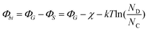 | (4) |
 | ||
| Fig. 2 Work function and layer number modulation. (a) Schematic of the band diagram with different graphene WF. As the WF increases, the built-in potential Φbi becomes larger, and more carriers are activated in graphene. (b) Calculated layer number dependence transmittance of graphene. (c) Calculated intrinsic graphene sheet resistance plots as a function of layer number. (d) Calculated Rsh–WF curves with different layer numbers. (e) Rsh–T relationship from simulation (solid line) and experiments (dashed line). | ||
The mechanism of tuning the WF of graphene (hence the sheet resistance Rsh) is rather straightforward. As shown in Fig. 2a, the dispersion of mobile π electrons in monolayer graphene near the Dirac point in the first Brillouin zone (BZ) is in a linear correlation (as Fig. 1c shows, the dispersion of mobile π electrons in multilayer graphene is not linear, but the following analysis still applies). For intrinsic graphene, the Fermi energy is located at the crossing point of the π and π* bands, which renders the carrier density at a low level at room temperature. However, if the Fermi energy is shifted away from the original position (see the lower diagram in Fig. 2a), more electrons or holes can be activated to participate in the conduction process. Therefore, graphene with shifted Fermi energy (i.e., modulated WF) performs better in conducting. Fig. 2d shows the theoretical analysis of the dependence of Rsh on WF, from which it is known that Rsh decreases significantly upon a tiny shift of WF from its intrinsic state.
The layer number (N) is another important parameter that influences both the transmittance and the sheet resistance of graphene, and thus determines the device performance. Fig. 2band c plot the calculated transmittance and the intrinsic sheet resistance of graphene as a function of layer number, respectively, using the method mentioned previously (ref. 38, eqn (3), and Section 1 in the ESI†). As the layer number increases, the sheet resistance decreases dramatically, which improves the cell performance, but the graphene film becomes less transparent, which in turn offsets the gains in cell performance.
Fig. 2e summarizes the Rsh–T curves of both the reported experimental data and our simulation results. Graphene films with varying WF in our calculation are presented in solid lines. The dashed lines plot the experimental data of graphene prepared through the roll-to-roll (R2R) process,40 interlayer-treated CVD-graphene (on copper) with HNO3,41 and undoped42 and AuCl3-doped43 CVD-graphene (on nickel). The CVD-graphene in Fig. 2d is found to be lightly p-doped. At the same transmittance, the experimental Rsh values are slightly larger than calculation, since the fabrication process inevitably introduces certain defects in graphene, leading to lower mobility, lower carrier density, and thus, higher resistivity.
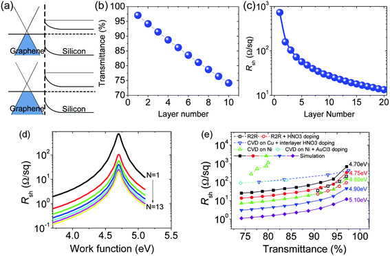
Because a large layer number might cause excessive light absorption whereas a small layer number is likely to attenuate the fill factor (FF), an optimal layer number corresponding to the best cell performance exists. Fig. 3a and b shows the efficiency and FF of devices with different WF as a function of the layer number of graphene. When the layer number is small, its increase may lead to a prominent improvement of FF; however, as the layer number becomes larger, such improvement becomes less significant. It is shown in Fig. 3a that a small layer number is needed to achieve the best cell performance when WF is large. The cell efficiency is calculated along the optimal line (dashed line in Fig. 3a). Over the WF range from 4.7 to 5.1 eV and at the optimized layer number, the efficiency varies from 0.6 to 6.0% and FF varies from 40.6 to 82.5% (see Fig. S8 in the ESI† for details).
 | ||
| Fig. 3 Theoretical analysis and experiment of the work function modulation of graphene/n-Si solar cells. (a) η and (b) FF as a function of graphene layer number. (c) Approaches to achieving WF modulation of graphene, including electric field effect,25 and chemical doping with viologen,34 AlOx,35 HNO3, SOCl2, and AuCl3.36 (d) Series resistance and (e) built-in potential change extracted from solar cell measurement results with various chemical treatment durations. | ||
The WF of graphene can be tuned either by an applied electric field or by proper chemical doping, as summarized in Fig. 3c. For example, AuCl3-doping can improve the WF to as high as 5.1 eV. We fabricated devices with various chemical treatments and measured their series resistances and built-in potential changes, which are plotted as a function of the chemical treatment time as shown in Fig. 3d and e. The series resistance decreases and the built-in potential increases at longer chemical treatment time. These changes reflect the modified WF. The effectiveness of the layer number optimization was not evaluated experimentally because the number of graphene layers could not be precisely controlled, especially for large-size graphene used in solar cell applications.
3.2 Antireflection (AR) technique
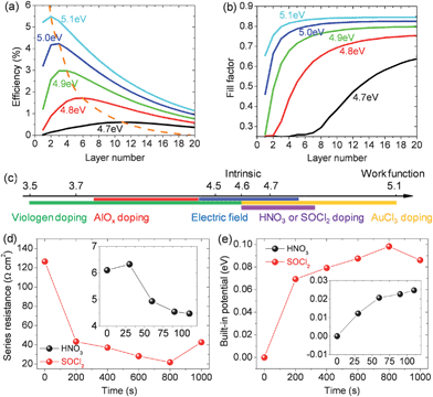
According to our theoretical model, the addition of an AR layer can also improve the cell performance. Several kinds of AR films have been used in the literature, such as a simple planar transparent film with optimized thickness and refraction index,44 a stratified planar film with gradually changing refraction index,45 a textured surface of the device,46 and some nanoscale light-trapping structure.47 However, none of these techniques possess both low cost and easy production process to address the reflection problem. We here report another novel AR technique. Through common lithography and etching process, the silicon substrate can be patterned into periodic pillar arrays. This simple method can significantly attenuate the optical reflection of the system, thus enhancing the photo-generated current and the conversion efficiency. Fig. 4a and b show the schematic diagram and optical photograph of the graphene/silicon-pillar-array (G/SiPA) device. The pillars are ∼2 μm in diameter and ∼2 μm in spacing, with heights ranging from 200 nm to 1 μm. Fig. 4c–e show scanning electron microscope (SEM) images of the pillar arrays with CVD graphene transferred on them. As graphene films are only several atoms thick, it is hard to recognize them in SEM. However, the wrinkles (see Fig. 4c and d) of graphene formed during the transfer process provide a way to observe the graphene surface. By this means, it can be observed that graphene and the pillar arrays are in good contact with each other not only on the top but also on the side walls of the pillars, which may also serve to increase the effective junction area of the device. Fig. 4f plots both the theoretical and experimental reflectance spectra in the ultraviolet-visible region of solar cells with planar Si and pillar-patterned Si. Theoretical calculation has predicted a reduction of AR reflectance to <5% by introducing the pillar array, whereas the experimental results show that the reflectance can be reduced from ∼45 to 25% using our simple AR method. The deviation of our calculations from the experiment results may be attributed to the non-idealities such as the surface contaminations introduced during fabrication or the unexpected oxidation layer that covers the silicon surface. In Fig. 4g, the experimental J–V curves of solar cells with and without pillar-array structure are plotted. The pillar-array structure (blue) exhibits a significantly larger short-circuit current (Jsc) than the cell with planar silicon (red), which confirms the effectiveness of our AR technique. | ||
| Fig. 4 Silicon-pillar-array antireflection. (a) The device schematic diagram and (b) photograph of the G/SiPA solar cell. (c) Top view, (d) side view and (e) low-magnification view of SEM images of the pillar array. (f) Calculated (dashed line) and measured (continuous line) reflection spectra of planar Si and Si-pillar-arrays with different etching depth. (g) Experimental J–V curves of solar cells with (blue) and without (red) pillar-array pattern. | ||
3.3 Improvement of the solar cell performance
Several typical graphene–silicon systems have been calculated and their critical parameters and simulation results are shown in Table 1 and Fig. 5a, respectively. In Fig. 5a, the energy loss is divided into four parts: (1) the reflection dissipation due to the reflectance of the air–graphene–substrate optical system; (2) the graphene absorption dissipation due to the energy absorption of graphene; (3) the conversion dissipation due to the energy loss (thermal relaxation, scattering, etc.) when electrons are excited by photons, and (4) the fill factor dissipation due to the “un-squareness” of the J–V curves. According to the calculations, sample 1 gives an efficiency of only 0.2% using intrinsic graphene (WF = 4.7 eV) and without AR treatment. The lightly doped sample 2 (without AR) and sample 3 (with pillar-array AR) have a WF approaching 4.8 eV. The reflectance of sample 3 drops to nearly 0 and the efficiency increases from 1.3 to 1.5% due to AR. Sample 4 has further optimized the layer number of graphene. Although Voc is slightly reduced, FF is raised by ∼50%, which improves the efficiency from 1.5 to 2.3%. Samples 4–6 reflect the improvement of solar cell performance by tuning the WF. Sample 6 has the largest WF (∼5.1 eV with AuCl3 doping43) and is predicted to give a considerably enhanced efficiency of ∼9.2%.| Samples | WF (eV) | N | R (%) | V oc (V) | J sc (mA cm−2) | FF (%) | η (%) | |
|---|---|---|---|---|---|---|---|---|
| a Abbreviations: G: graphene; NAR: non-AR; PA-AR: pillar-array AR; OLN: optimized layer number; N: layer number of graphene. | ||||||||
| 1 | Pure G, NAR | 4.7 | 3 | 39.0 | 0.38 | 2.3 | 25.2 | 0.2 |
| 2 | CVD-G, NAR | 4.8 | 3 | 39.0 | 0.49 | 8.9 | 30.2 | 1.3 |
| 3 | CVD-G, PA-AR | 4.8 | 3 | 0.01 | 0.51 | 11.2 | 25.6 | 1.5 |
| 4 | CVD-G, PA-AR, OLN | 4.8 | 5 | 0.01 | 0.50 | 12.3 | 37.7 | 2.3 |
| 5 | Doped-G, PA-AR, OLN | 4.9 | 3 | 0.01 | 0.67 | 14.7 | 59.1 | 5.8 |
| 6 | AuCl3-G, PA-AR, OLN | 5.1 | 2 | 0.01 | 0.84 | 16.1 | 68.2 | 9.2 |
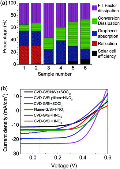 | ||
| Fig. 5 Summary of simulation and experimental results. (a) Efficiency and percentages of dissipation by reflection, graphene-absorption, conversion and FF. (b) J–V curves of solar cells based on CVD-graphene/Si (G/Si) nanowires with SOCl2 doping (blue),49 CVD-G/Si pillar-array with HNO3 doping (violet), CVD-G/Si with SOCl2 doping (red),50 flame-G/Si with HNO3 doping (dark green),31 and CVD-G/Si with HNO3 doping (magenta). | ||
Typical experimental results are summarized in Table 2 and Fig. 5b. The graphene films were grown either by CVD22 or by the flame method,31 and the substrates included silicon nanowires (SiNWs), silicon pillar array and polished silicon, either treated with thionyl chloride (SOCl2) or nitric acid (HNO3). For example, HNO3 treatment was found to improve the cell efficiency up to 5.38% (graphene: 3–5 layers). This result is comparable with our theoretically calculated value (sample 5 in Table 1). The cell based on thinner graphene (2–3 layers) shows a maximum efficiency of 7.7% upon acid doping. Fig. 6 compares the theoretical and experimental efficiencies of our solar cells with those of reported graphene-based solar devices, including bulk heterojunction organic photovoltaic devices (OPVs) and graphene/CdS or CdSe nanostructure solar cells.
| Samples | V oc (V) | J sc (mA cm−2) | FF (%) | η (%) |
|---|---|---|---|---|
| CVD-G/SiNWs + SOCl2 (ref. 49) | 0.503 | 11.24 | 50.6 | 2.86 |
| CVD-G/Si pillars + HNO3 | 0.495 | 17.33 | 50.8 | 4.35 |
| CVD-G/Si + SOCl2 (ref. 50) | 0.517 | 13.20 | 58.0 | 3.93 |
| Flame-G/Si + HNO3 (ref. 31) | 0.530 | 13.75 | 59.7 | 4.35 |
| CVD-G/Si + HNO3 | 0.510 | 17.57 | 60.1 | 5.38 |
| CVD-G/Si + HNO3 | 0.515 | 22.70 | 66.0 | 7.72 |
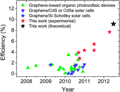 | ||
| Fig. 6 Summary and efficiency comparison of various graphene-based solar cells. The efficiency of our device is the highest among all of them. References cited in the figure are listed in the ESI.† | ||
As a demonstration, the graphene/Si-pillar-array solar cell has been used as a light sensor. The solar device is connected to a signal amplifier circuit to power a liquid crystal display screen (see Fig. S9 in the ESI†), which is transparent under high voltage and opaque under low voltage. The screen can be switched on and off by tuning the illumination intensity. Given the discontinuity of the graphene films used in our experiments, we believe that the cell performance can be improved further to reach the theoretical maximum.
4 Conclusions
To conclude, we have proposed a simple model for graphene/semiconductor heterojunction solar devices. According to the model analysis, the device performance can be improved by using an antireflection technique and by modifying the work function of graphene. Based on our theoretical calculation with key modification treatments, the conversion efficiency reaches ∼9.2%. Among the proposed treatments, the array-pattern process can practically improve the cell efficiency. Solar cells based on modified graphene and Si pillar arrays have been fabricated and are found to deliver enhanced cell performance with efficiencies of up to 7.7%. Recent studies have realized a local layer-by-layer removal technique to accurately control the layer number of graphene.48 These results, together with the chemical doping process mentioned previously, promise great potentials in graphene electrode modulation and hence deserve further investigation.Acknowledgements
This work was supported by the National Science Foundation of China (51072089, 50972067, 61025021, 60936002), the Tsinghua National Laboratory for Information Science and Technology (TNList) the Cross-discipline Foundation, National Key Project of Science and Technology (2009ZX02023-001-3), the International Cooperation Project from Ministry of Science and Technology of China (2008DFA12000) and the National Program on Key Basic Research Project (2011CB013000).References
- A. K. Geim and K. S. Novoselov, The rise of graphene, Nat. Mater., 2007, 6, 183–191 CrossRef CAS.
- X. Huang, X. Y. Qi, F. Boey and H. Zhang, Graphene-based composites, Chem. Soc. Rev., 2012, 41, 666–666 RSC.
- X. Huang, Z. Yin, S. Wu, X. Qi, Q. He, Q. Yan, F. Boey and H. Zhang, Graphene-based materials: synthesis, characterization, properties and applications, Small, 2011, 7, 1876–1902 CrossRef CAS.
- K. S. Novoselov, A. K. Geim, S. V. Morozov, D. Jiang, M. I. Katsneison, I. V. Grigorieva, S. V. Dubonos and A. A. Firsov, Two-dimensional gas of massless Dirac fermions in graphene, Nature, 2005, 438, 197–200 CrossRef CAS.
- A. Fasolino, J. H. Los and M. I. Katsnelson, Intrinsic ripples in graphene, Nat. Mater., 2007, 6, 858–861 CrossRef CAS.
- C. Lee, X. Wei, J. W. Kysar and J. Hone, Measurement of the elastic properties and intrinsic strength of monolayer graphene, Science, 2008, 321, 385–388 CrossRef CAS.
- A. A. Balandin, Thermal properties of graphene and nanostructured carbon materials, Nat. Mater., 2011, 10, 569–581 CrossRef CAS.
- D. L. Nika, S. Ghosh, E. P. Pokatilov and A. A. Balandin, Lattice thermal conductivity of graphene flakes: comparison with bulk graphite, Appl. Phys. Lett., 2009, 94, 203103 CrossRef.
- D. L. Nika, E. P. Pokatilov, A. S. Askerov and A. A. Balandin, Phonon thermal conduction in graphene: role of Umklapp and edge roughness scattering, Phys. Rev. B: Condens. Matter Mater. Phys., 2009, 79, 155413 CrossRef.
- R. R. Nair, P. Blake, A. N. Grigorenko, K. S. Novoselov, T. J. Booth, T. Stauber, N. M. R. Peres and A. K. Geim, Fine structure constant defines visual transparency of graphene, Science, 2008, 320, 1308 CrossRef CAS.
- Y.-M. Lin, H.-Y. Chiu, K. A. Jenkins, D. B. Farmer, P. Avouris and A. Valdes-Garcia, Dual-gate graphene FETs with fT of 50 GHz, IEEE Electron Device Lett., 2010, 31, 68–70 CrossRef CAS.
- Q. Y. He, S. X. Wu, S. Gao, X. H. Cao, Z. Y. Yin, P. Chen and H. Zhang, Transparent, flexible, all-reduced graphene oxide thin film transistors, ACS Nano, 2011, 5, 5038–5044 CrossRef CAS.
- Q. Y. He, H. G. Sudibya, Z. Y. Yin, S. X. Wu, H. Li, F. Boey, W. Huang, P. Chen and H. Zhang, Centimeter-long and large-scale micropatterns of reduced graphene oxide films: fabrication and sensing applications, ACS Nano, 2010, 4, 3201–3208 CrossRef CAS.
- Y. Ouyang, H. Dai and J. Guo, Projected performance advantage of multilayer graphene nanoribbons as a transistor channel material, Nano Res., 2010, 3, 8–15 CrossRef CAS.
- X. Yang, G. Liu, A. A. Balandin and K. Mohanram, Triple-mode single-transistor graphene amplifier and its applications, ACS Nano, 2010, 4, 5532–5538 CrossRef CAS.
- J. T. Robinson, M. Zalalutdinov, J. W. Baldwin, E. S. Snow, Z. Wei, P. Sheehan and B. H. Houston, Wafer-scale reduced graphene oxide films for nanomechanical devices, Nano Lett., 2008, 8, 3441–3445 CrossRef CAS.
- Y. Zheng, G.-X. Ni, C.-T. Toh, M.-G. Zeng, S.-T. Chen, K. Yao and B. Özyilmaz, Gate-controlled nonvolatile graphene-ferroelectric memory, Appl. Phys. Lett., 2009, 94, 163505 CrossRef.
- J. Q. Liu, Z. Y. Yin, X. H. Cao, F. Zhao, A. P. Lin, L. H. Xie, Q. L. Fan, F. Boey, H. Zhang and W. Huang, Bulk heterojunction polymer memory devices with reduced graphene oxide as electrodes, ACS Nano, 2010, 4, 3987–3992 CrossRef CAS.
- P. Blake, P. D. Brimicombe, R. R. Nair, T. J. Booth, D. Jiang, F. Schedin, L. A. Ponomarenko, S. V. Morozov, H. F. Gleeson, E. W. Hill, A. K. Geim and K. S. Novoselov, Graphene-based liquid crystal device, Nano Lett., 2008, 8, 1704–1708 CrossRef.
- G. Jo, M. Choe, C.-Y. Cho, J. H. Kim, W. Park, S. Lee, W.-K. Hong, T.-W. Kim, S.-J. Park, B. H. Hong, Y. H. Kahng and T. Lee, Large-scale patterned multi-layer graphene films as transparent conducting electrodes for GaN light-emitting diodes, Nanotechnology, 2010, 21, 175201 CrossRef.
- H. Park, J. A. Rowehl, K. K. Kim, V. Bulovic and J. Kong, Nanotechnology, 2010, 21, 505204 CrossRef.
- X. M. Li, H. W. Zhu, K. L. Wang, A. Y. Cao, J. Q. Wei, C. Y. Li, Y. Jia, Z. Li and D. H. Wu, Graphene-on-silicon Schottky junction solar cells, Adv. Mater., 2010, 22, 2743–2748 CrossRef CAS.
- Q. Shao, G. Liu, D. Teweldebrhan and A. A. Balandin, High-temperature quenching of electrical resistance in graphene interconnects, Appl. Phys. Lett., 2008, 92, 202108 CrossRef.
- X. Chen, D. Akinwande, K.-J. Lee, G. F. Close, S. Yasuda, B. C. Paul, S. Fujita, J. Kong and H.-S. P. Wong, Fully integrated graphene and carbon nanotube interconnects for gigahertz high-speed CMOS electronics, IEEE Trans. Electron Devices, 2010, 57, 3137–3143 CrossRef CAS.
- S. Ghosh, I. Calizo, D. Teweldebrhan, E. P. Pokatilov, D. L. Nika, A. A. Balandin, W. Bao, F. Miao and C. N. Lau, Extremely high thermal conductivity of graphene: prospects for thermal management applications in nanoelectronic circuits, Appl. Phys. Lett., 2008, 92, 151911 CrossRef.
- Y. Y. Shao, J. Wang, H. Wu, J. Liu, I. A. Aksay and Y. H. Lin, Electroanalysis, 2010, 22, 1027–1036 CrossRef CAS.
- N. Motanty and V. Berry, Graphene-based single-bacterium resolution biodevice and DNA transistor: interfacing graphene derivatives with nanoscale and microscale biocomponents, Nano Lett., 2008, 8, 4469–4476 CrossRef.
- Q. Y. He, S. X. Wu, Z. Y. Yin and H. Zhang, Graphene-based electronic sensors, Chem. Sci., 2012, 3, 1764–1772 RSC.
- M. He, J. H. Jung, F. Qiu and Z. Q. Lin, Graphene-based transparent flexible electrodes for polymer solar cells, J. Mater. Chem., 2012, 22, 24254 RSC.
- Z. Y. Yin, S. Y. Sun, T. Salim, S. X. Wu, X. Huang, Q. Y. He, Y. M. Lam and H. Zhang, Organic photovoltaic devices using highly flexible reduced graphene oxide films as transparent electrodes, ACS Nano, 2010, 4, 5263–5268 CrossRef CAS.
- Z. Li, H. W. Zhu, D. Xie, K. L. Wang, A. Y. Cao, J. Q. Wei, X. Li, L. L. Fan and D. H. Wu, Flame synthesis of few-layered graphene/graphite films, Chem. Commun., 2011, 47, 3520–3522 RSC.
- K. Ihm, J. T. Lim, K.-J. Lee, J. W. Kwon, T.-H. Kang, S. Chung, S. Bae, J. H. Kim, B. H. Hong and G. Y. Yeom, Number of graphene layers as a modulator of the open-circuit voltage of graphene-based solar cell, Appl. Phys. Lett., 2010, 97, 032113 CrossRef.
- Y.-J. Yu, Y. Zhao, S. Ryu, L. E. Brus, K. S. Kim and P. Kim, Tuning the graphene work function by electric field effect, Nano Lett., 2009, 9, 3430–3434 CrossRef CAS.
- H. K. Jeong, K.-J. Kim, S. M. Kim and Y. H. Lee, Modification of the electronic structure of graphene by viologen, Chem. Phys. Lett., 2010, 498, 168–171 CrossRef CAS.
- Y. Yi, W. M. Choi, Y. H. Kim, J. W. Kim and S. J. Kang, Effective work function lowering of multilayer graphene films by subnanometer thick AlOx overlayers, Appl. Phys. Lett., 2011, 98, 013505 CrossRef.
- Y. Shi, K. K. Kim, A. Reina, M. Hofmann, L.-J. Li and J. Kong, Work function engineering of graphene electrode via chemical doping, ACS Nano, 2010, 4, 2689–2694 CrossRef CAS.
- C.-H. Sun, P. Jiang and B. Jiang, Broadband moth-eye antireflection coatings on silicon, Appl. Phys. Lett., 2008, 92, 061112 CrossRef.
- T. Stauber, N. M. R. Peres and A. K. Geim, Optical conductivity of graphene in the visible region of the spectrum, Phys. Rev. B: Condens. Matter Mater. Phys., 2008, 78, 085432 CrossRef.
- W. C. Chew, Waves and Fields in Inhomogeneous Media, Wiley-IEEE Press, 1999 Search PubMed.
- S. Bae, H. Kim, Y. Lee, X. Xu, J.-S. Park, Y. Zheng, J. Balakrishnan, T. Lei, H. R. Kim, Y. I. Song, Y.-J. Kim, K. S. Kim, B. Özyimaz, J.-H. Ahn, B. H. Hong and S. Iijima, Roll-to-roll production of 30-inch graphene films for transparent electrodes, Nat. Nanotechnol., 2010, 5, 574–578 CrossRef CAS.
- A. Kasry, M. A. Kuroda, G. J. Martyna, G. S. Tulevski and A. A. Bol, Chemical doping of large-area stacked graphene films for use as transparent, conducting electrodes, ACS Nano, 2010, 4, 3839–3844 CrossRef CAS.
- K. S. Kim, Y. Zhao, H. Jang, S. Y. Lee, J. M. Kim, K. S. Kim, J.-H. Ahn, P. Kim, J.-Y. Choi and B. H. Hong, Large-scale pattern growth of graphene films for stretchable transparent electrodes, Nature, 2009, 457, 706–710 CrossRef CAS.
- K. K. Kim, A. Reina, Y. Shi, H. Park, L.-J. Li, Y. H. Lee and J. Kong, Enhancing the conductivity of transparent graphene films via doping, Nanotechnology, 2010, 21, 285205 CrossRef.
- D. L. Brundrett, E. N. Glytsis and T. K. Gaylord, Homogeneous layer models for high-spatial frequency dielectric surface-relief gratings: conical diffraction and antireflection designs, Appl. Opt., 1994, 33, 2695–2706 CrossRef CAS.
- Y. Asahara and T. Izumitani, The properties of gradient index antireflection layer on the phase separable glass, J. Non-Cryst. Solids, 1980, 42, 269–279 CrossRef CAS.
- J. H. Zhao, A. H. Wang, M. A. Green and F. Ferrazza, 19.8% efficient “honeycomb” textured multicrystalline and 24.4% monocrystalline silicon solar cells, Appl. Phys. Lett., 1998, 73, 1991 CrossRef CAS.
- M. D. Kelzenberg, S. W. Boettcher, J. A. Petykiewicz, D. B. Turner-Evans, M. C. Putnam, E. L. Warren, J. M. Spurgeon, R. M. Briggs, N. S. Lewis and H. A. Atwater, Enhanced absorption and carrier collection in Si wire arrays for photovoltaic applications, Nat. Mater., 2010, 9, 239–244 CrossRef CAS.
- A. Dimiev, D. V. Kosynkin, A. Sinitskii, A. Slesarev, Z. Sun and J. M. Tour, Layer-by-layer removal of graphene for device patterning, Science, 2011, 331, 1168–1172 CrossRef CAS.
- G. F. Fan, H. W. Zhu, K. L. Wang, J. Q. Wei, X. M. Li, Q. K. Shu, N. Guo, X. Li and D. H. Wu, Graphene/silicon nanowire Schottky junction for enhanced light harvesting, ACS Appl. Mater. Interfaces, 2011, 3, 721–725 CAS.
- X. M. Li, H. W. Zhu, K. L. Wang, J. Q. Wei, G. F. Fan, X. Li and D. H. Wu, Chemical doping and enhanced solar energy conversion of graphene–silicon junction, in Proceedings of the conference on China technological development of renewable energy source, 2010, vol. I, pp. 387–390 Search PubMed.
Footnotes |
| † Electronic supplementary information (ESI) available: Simulation details. See DOI: 10.1039/c2ee23538b |
| ‡ These authors contributed equally to this work. |
| This journal is © The Royal Society of Chemistry 2013 |