Engineering of efficiency limiting free carriers and an interfacial energy barrier for an enhancing piezoelectric generation†
Jung Inn
Sohn
ad,
Seung Nam
Cha
*ad,
Byong Gwon
Song
ab,
Sanghyo
Lee
b,
Seong Min
Kim
a,
JiYeon
Ku
a,
Hyun Jin
Kim
a,
Young Jun
Park
a,
Byoung Lyong
Choi
a,
Zhong Lin
Wang
c,
Jong Min
Kim
*ad and
Kinam
Kim
a
aFrontier Research Lab., Samsung Advanced Institute of Technology, Yongin, 449-712, Korea
bDepartment of Physics, Hanyang University, Seoul, 133-791, Korea
cSchool of Materials Science and Engineering, Georgia Institute of Technology, Atlanta, Georgia 30332-0245, USA
dDepartment of Engineering Science, University of Oxford, Oxford, OX1 3PJ, UK. E-mail: seungnam.cha@eng.ox.ac.uk; jong.kim@eng.ox.ac.uk
First published on 21st November 2012
Abstract
The energy harvesting efficiency is of tremendous importance for the realization of a high output-power nanogenerator serving as the basis for self-powered electronics. Here we report that the device performance of a sound-driven piezoelectric energy nanogenerator (SPENG) is remarkably improved by controlling both the carrier density and the interfacial energy in a semiconducting ZnO nanowire (NW), thereby achieving its intrinsic efficiency limits. A SPENG with carrier-controlled ZnO NWs exhibits excellent energy harvesting characteristics with an average power density of 0.9 mW cm−3, as well as a near 50 fold increase in both output voltage and current compared to those of a conventional ZnO NW. In addition, we demonstrate for the first time that an optimized SPENG is large enough and very suitable to drive electrophoretic ink displays based on voltage-drive systems. This fundamental progress makes it possible to fabricate high performance nanogenerators for viable industrial applications in portable/wearable personal electronics such as electronic papers and smart identity cards.
Broader contextThe ability to control and manipulate both the carrier dynamics and the interfacial energy in semiconductor-based energy harvesting materials is of tremendous importance for optimizing their energy efficiency. Remarkable improvements in the device performance of a piezoelectric nanogenerator, with a piezoelectric semiconducting nanowire array, can be achieved through a combination of doping and surface modification schemes to suppress the undesirable screening effect of the free carriers. In addition, the output performance is further enhanced and maximized by the incorporation of a functional interlayer, effectively obstructing free carriers from passing through the metal–semiconductor interface. In this work, we optimized nanogenerator performance with excellent piezoelectric characteristics through the engineering of efficiency limiting free carriers and an interfacial energy barrier and demonstrated that the power of the optimized nanogenerator is sufficient to drive electrophoretic displays. This approach is expected to be an attractive potential strategy, providing the high possibility for realizing multi-functional, self-powered devices with high performances. |
The anticipated increasing use of key natural energy resources, which become extremely scarce, in the coming decades have sparked significant world-wide efforts toward the search for cost-effective, renewable and green energy sources to meet the global energy demands of the future.1–5 In this regard, advances in self-powered nanotechnology, that allow for the design of efficient energy harvesting, offer an enormous potential for the creation of sustainable systems utilizing unlimited natural ambient energy sources.6–10
Recent developments in piezoelectric power generators harvesting energy steadily from ambient mechanical vibrations without regard to time, place, or any external conditions, present innovative and emerging research topics in the area of a green energy technology.6,10,11,13 In particular, a ZnO nanowire (NW) has been intensively studied as one of the most attractive piezoelectric materials for widespread use as a clean and inexhaustible power source in future self-powered nanosystems, including implantable chips, flexible/portable electronics, and environmental and heath monitoring sensors, because of its unique dimensionality and superior transparent and piezoelectric semiconducting properties coupled with biocompatibility, environmental friendliness, and geometrical versatility.6,10,11
To date various approaches have been reported demonstrating and enhancing unique capabilities for a ZnO NW-based piezoelectric energy generator by introducing various NW arrays and device configurations, flexible/textile electrodes and substrates, and diverse types of ambient mechanical energy sources.6,11,13–17 However, despite the demonstrated ability and fascinating piezoelectric features of ZnO NWs, there are serious impediments to the device performance, as well as to a detailed understanding of the underlying physics that account for the energy harvesting mechanism, because free charge carriers in ZnO NWs, unlike in ideal insulating piezoelectric materials,18–20 partially screen piezoelectrically generated immobile charges. That is, when a mechanical force is applied on a ZnO NW, free electrons in the conduction band flow into piezoelectric potential areas to balance the piezoelectric potential, leaving depleted ionized donors in the negative potential area and accumulated electrons in the positive potential area of the NW.11,12 Furthermore, an imperfect energy barrier between the metal electrode and the piezoelectric semiconductor, which causes the leakage current through the metal–semiconductor (MS) interface and hence results in a decrease in the piezoelectric potential, poses another outstanding difficulty to be overcome for maximizing the efficiency of piezoelectric energy harvesting.6,10,17 Thus, in order to extend the feasibility of semiconductor based piezoelectric energy generators to practical applications, it is necessary to seek a potential solution to the problem of the reduction of the piezoelectric potential through engineering efficiency limiting free carrier density and/or the interfacial energy barrier. In addition to the issues of enhancement of device performance in piezoelectric energy generators, recognizing and establishing ideal applications for those, which generate substantial output voltage yet limited output current, is another crucial issue to be addressed. For this, self-powered electronics, possessing favorable power consumption characteristics without the need of a constant current supply, can be considered as viable commercial applications. Electrophoretic ink displays are especially suitable voltage-drive systems as they require power not to maintain but only to change images, and we demonstrate, for the first time, a fully self-powered display system.
The operation principle of a sound-driven piezoelectric energy nanogenerator (SPENG) and the dependence of piezopotentials for different donor concentrations are presented in Fig. 1. The energy harvesting functionality of ZnO NWs arises from the modulation of the piezoelectric polarization when the mechanical force is applied on the NW, which induces the relative displacement of the Zn cations with respect to the O anions along the strain direction.10 The piezoelectric effect produces ionic charges distributed along the NW and hence results in the piezoelectric field. This field drives free electrons to flow in an external circuit to balance the piezoelectric potential generated across the two ends of a NW. Therefore, the piezoelectric current is directly dependent on the piezoelectric potential. Consequently, the negative piezoelectric potential developed on the compressed top side of a NW by the sonic wave leads to the accumulation of electrons on the bottom side (middle of Fig. 1a), whereas, when the external force is released, the accumulated electrons on the bottom side flow back to the top side (right of Fig. 1a) through the external circuit in order to balance the difference in Fermi levels at the two sides.13 Thus we believe that ZnO NWs clearly function as a basis for a nanogenerator producing the output piezoelectric voltage and current by mechanical vibrations causing alternating tensile and compressive strains. However, in contrast to insulating piezoelectric materials, the effective piezoelectric potential of a semiconducting ZnO is generated as a result of competition between piezoelectrically generated ionic charges and the free charges screening them. This causes the detrimental effect of free charges on the generation of electric potential, even though the ZnO is more effective for energy harvesting because of its low permittivity.
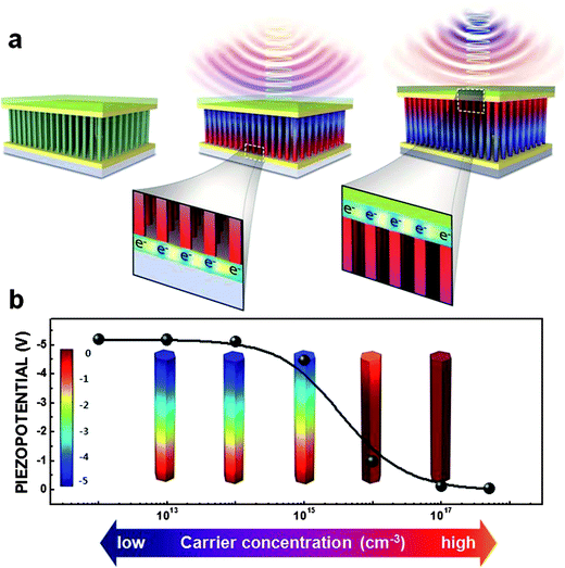 | ||
| Fig. 1 Operation principle of a SPENG and calculated piezopotential distributions of a semiconducting ZnO NW for different donor concentrations. (a) When the compressive strain is induced on the top side of a NW by the sonic wave, the negative potential is developed on the top side (middle). Subsequently, this piezopotential drives a flow of electrons in an external circuit and leads to the accumulation of electrons on the bottom side. Conversely, when the external force is released from the top side, the electrons accumulated on the top side flow back through the external circuit in order to neutralize the positive piezopotential generated by the tensile stress on the top side (right). (b) Calculated piezopotential differences in a ZnO NW vertically exerted along the NW length by a constant external force induced on the top side as a function of donor concentrations ranging from 1012 to 5 × 1017 cm−3 and corresponding three-dimensional piezopotential distributions of a NW, respectively. | ||
The ability to control the charge carrier density enables us to suppress the undesirable screening effect of the free carriers, which is extremely important in optimizing the efficiency and total output power towards the fundamental limits of intrinsic ZnO. For this reason, we first performed the simulation of piezoelectric potential distributions in ZnO NWs with a donor concentration ranging from 1012 (relatively low) to 5 × 10¹⁷ (relatively high) cm−3 by using the COMSOL package as shown in Fig. 1b (also see ESI† for the calculation of the piezoelectric potential). It is clearly shown that the higher the carrier concentration, the more pronounced the screening effect is due to the free charges and thus the smaller the piezoelectrically generated charge is, leading to a large reduction in the piezopotential, that is, a few tens of magnitude between relatively low and high doping levels. Interestingly, above the high carrier density regime (>5 × 1017 cm−3), charges generated by the piezoelectric effect are almost completely cancelled, which can obliterate any piezoelectric potential. These results indicate that the piezoelectric characteristic of a semiconducting NW is significantly influenced by the free charge carriers, which screen piezoelectrically generated charges. This in turn implies that one of the rational ways to overcome such detrimental effects resulting from the free carriers is to decrease free carriers by utilizing doping.
To this end, a doping method was employed to modulate donor concentrations by introducing p-type dopants. Li-doped ZnO NWs have been prepared in aqueous solution with varying Li molar concentrations from 12.5 to 100 mM as a favorable and stable p-type dopant source, as shown in Fig. 2a, using a hydro-thermal method reported previously (see Methods).21,22 (ZnO NWs grown under a 12.5 mM concentration is referred to as “12.5 mM Li-doped ZnO NWs”, and so on.) Cross-sectional scanning electron microscopy (SEM) images show that all NWs grown under different Li molar concentrations exhibit the same crystallographic growth direction, resulting in a highly oriented vertical NW array having quite similar average lengths of ∼2.5 μm as shown in the inset of Fig. 2e. The incorporation of Li dopants into ZnO has been clearly revealed by photoluminescence (PL) examinations, as shown in Fig. 2b, which are an ideal and powerful technique to precisely observe dopant related emissions. It is further revealed that the spectrum of a 12.5 mM Li-doped ZnO NWs with a relatively low acceptor concentration is dominated by a neutral donor-bound exciton (D0X), which is attributed to the presence of a relatively large amount of donors. In contrast, clear characteristic features of acceptor related emissions, which correspond to neutral acceptor-bound exciton (A0X) peaks, as well as free electrons to the acceptor (FA) and donor to acceptor pair (DAP) transitions, are observed in the moderate Li concentration regime, that is, 25 and 50 mM. This finding provides a strong evidence that the Li atoms substitute Zn atoms, which is theoretically expected to be a shallow acceptor.22 In addition, in the relatively high Li concentration regime (100 mM), we observed a decrease in intensity of DAP and FA peaks, which is attributed to excessive incorporation of Li atoms resulting from high Li contents.23 We further confirmed the assignment of acceptor related peaks by analyzing the evolution of PL spectra obtained at the low temperatures of 10–300 K (Fig. 2c), which unambiguously exhibited the formation of shallow acceptors in ZnO doped by Li and fitted well with Varshni's formula shown in Fig. 2d and S1.†24 Spatial distribution and relative contents of Li atoms in NWs were also confirmed by secondary ion mass spectroscopy (SIMS) as shown in ESI Fig. S2,† which is consistent with the PL results.
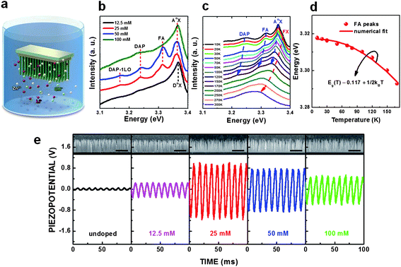 | ||
| Fig. 2 Evaluation of Li-doped ZnO NWs. (a) Schematic of the hydro-thermal growth for Li-doped ZnO NWs. (b) PL spectra at 10 K for Li-doped ZnO NW samples with various Li concentrations. (c) The temperature-dependent PL spectra of a 25 mM Li-doped ZnO NW sample, showing the evolution of acceptor related emission peaks. (d) The temperature dependence of FA peak energy positions obtained for a 25 mM Li-doped ZnO NW sample. The solid line is the fitting curve using Varshni's formula. Here, note that the acceptor energy of Ea in ZnO is calculated to be about 117 meV based on the following equation: EFA(T) = Eg(T) − Ea + 0.5KbT, where Kb is the Boltzmann constant. (e) Piezopotential measured from a SPENG consisting of ITO coated flexible PES as a top electrode and Li-incorporated NWs ranging from 0 (undoped) to 100 mM. (Top inset) cross-sectional SEM images of vertically well-aligned ZnO NW arrays grown on a ZnO film (50 nm) coated Si substrate under different Li molar concentrations. The scale bar is 2 μm for all images. | ||
In order to assess whether free charge carriers can affect the piezoelectric characteristics of ZnO NWs, we performed piezopotential measurements of a SPENG with ZnO NWs incorporated with a Li dopant source ranging from 0 (undoped) to 100 mM by applying sonic waves with the input of 100 dB at a sweep frequency of 100 Hz. Noticeably, a considerable enhancement in piezoelectric output voltages, as shown in Fig. 2e, and currents (see ESI, Fig. S3†) was observed after the incorporation of Li dopants into ZnO NWs, which was attributed to a reduction in free carrier concentrations. In general, it is well known that an as-grown ZnO NW is naturally n-type semiconducting with superior conductivity because of oxygen deficiencies.25 Thus, note that electrons in an undoped NW significantly screen piezoelectric charges and hence cause extremely low output piezopotential, showing the difference of a few orders of magnitude between theoretically expected and experimentally observed values. Interestingly, we also observed that the output voltage is correspondingly enhanced with Li concentrations up to 25 mM because of a continuous decrease in donor concentrations as expected from our calculation (Fig. 1b), whereas the output voltage is gradually reduced with further increasing Li concentrations due to the compensation effect, such as the formation of acceptor complexes, deep levels, and interstitials, resulting from higher Li concentrations.23 This is consistent with the PL (as shown in Fig. 2b) and SIMS results. These results indicate that piezoelectric output power is strongly dependent upon free charges, which is thought to be a critical consideration for optimizing piezoelectric performance towards the theoretical limits by suppressing the detrimental effects of free carriers.
To further verify whether a large discrepancy in piezoelectric performance between theory and experiments originates from free charge carriers, we also investigated the surface functionalization of ZnO NWs both with and without Li dopants by introducing oleic acid. A negatively charged carboxylic group of oleic acid molecules induces an electrostatic potential, which can alter and affect surface charge states of NWs and hence result in a significant change in electrical conductivity and free carrier concentrations of the NWs.25,26 The first evidence for the successful functionalization of a ZnO NW came from electrical transfer measurements with a ZnO NW field-effect transistor (FET) as shown in Fig. 3a. It is evident that after oleic acid surface modification, the conductance of a modified ZnO NW FET is reduced compared with the unmodified ZnO NW FET and that the threshold voltage is shifted towards a positive gate voltage direction, which is attributed to the negatively charged carboxylic functional group bonded on the surface causing a surface potential change and band bending.25 This results in a depletion of electrons from a ZnO NW, leading to a positive shift in the threshold voltage and a decrease in the carrier concentration. Note that we also confirmed that the NWs were indeed functionalized with oleic acid using FT-IR spectroscopy and X-ray photoelectron spectroscopy (XPS) examinations (see ESI, Fig. S4 and S5†). Furthermore, similar to electrical transfer characteristics of a ZnO NW FET, our simulations reveal that the presence of negatively charged molecules on a ZnO NW surface causes a large enhancement of the piezoelectric potential due to the depletion of electrons in a NW as shown in Fig. 3b.
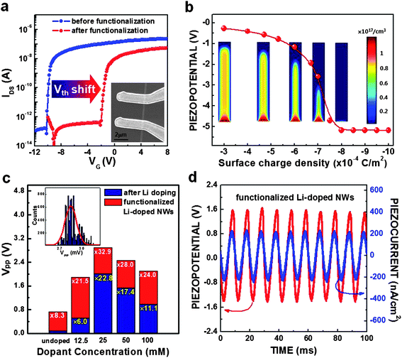 | ||
Fig. 3 Piezoelectric characteristics of functionalized ZnO NWs. (a) Transfer characteristics of ZnO NW FETs measured at a drain bias of 0.1 V before and after oleic acid surface functionalization. The inset is a SEM image of a ZnO NW between source and drain electrodes. (b) Calculated piezopotential differences and distributions of a ZnO NW vertically compressed along the NW length by a constant external force induced on the top side as a function of the surface charge density. (Inset) Corresponding carrier density distributions of a NW. The numbers indicate an enhanced magnitude of output voltages for Li-doped NWs without (yellow) and with (white) the functionalized surface layer, respectively, compared to that of undoped NWs without the functionalized surface layer. (c) Histogram of piezoelectric output voltages for undoped and Li-doped ZnO NW samples before (blue) and after (red), respectively. Numbers indicate an enhanced magnitude of output voltages after Li-doping (yellow) and functionalization (white), respectively. The inset shows statistical data for 10![[thin space (1/6-em)]](https://www.rsc.org/images/entities/char_2009.gif) 000 peak-to-peak voltages measured from a SPENG with functionalized 25 mM Li-doped ZnO NWs. (d) The piezoelectric output potential and current simultaneously measured from a SPENG consisting of integrated 25 mM Li-doped ZnO NWs with the oleic acid layer. 000 peak-to-peak voltages measured from a SPENG with functionalized 25 mM Li-doped ZnO NWs. (d) The piezoelectric output potential and current simultaneously measured from a SPENG consisting of integrated 25 mM Li-doped ZnO NWs with the oleic acid layer. | ||
To investigate the energy harvesting capabilities of functionalized NWs, we directly compared piezoelectric output voltages of SPENGs with undoped and Li-doped ZnO NW before and after the surface functionalization, respectively, as summarized in the histogram of Fig. 3c. Here, we note that for a more accurate statistical comparison, maximum average piezoelectric voltages were obtained from each device by the Gaussian fitting of 10000 measured peak-to-peak voltages showing a standard deviation of only 7% (the inset of Fig. 3c). As expected, we clearly observed that the piezoelectric potential of all devices was improved after the surface functionalization of ZnO NWs regardless of Li-doping concentrations due to the complementary effects of doping and surface modification resulting in a decrease in the carrier concentration (see ESI, Fig. S6†). In particular, it has been demonstrated that functionalized 25 mM Li-doped ZnO NWs produce a peak-to-peak output voltage up to 2.9 V, which is over 30 times higher than that of undoped NWs without the functionalized surface layer. This large magnitude of enhancement in piezopotential is consistent with our simulation results presented in Fig. 1b and 3b. Interestingly, in contrast to piezoelectric properties shown in Fig. 2e, the enhancement of the average output voltages is more effective for undoped and relatively low for Li-doped samples, that is, a larger increase in the average output voltage was observed at the high donor concentrations after the surface modification with charged molecules compared to moderate and high Li-doped samples with relatively low donor concentrations (Fig. 2b). This implies that the lower the Li dopant is, the higher the donor concentration (i.e. free electron concentration) is and hence the more electrons are depleted after the surface functionalization, causing a relatively larger enhancement of piezoelectric potential. This is because Li doping reduces the free electrons in ZnO and the surface functionalization further reduces them. These findings indicate that the amount of depletion of free carriers plays a significant role in determining the output voltage.
Fig. 3d shows the piezoelectric potential and current of a nanogenerator consisting of integrated Li-doped ZnO NWs with the negatively charged-oleic acid layer, which were simultaneously measured by applying sinusoidal sonic input signals with a sensitivity of 100 dB at 100 Hz. It is clear from the shape and position of the generated alternating output signals that the measured signals were originally from a SPENG and that there is a negligible phase angle difference between corresponding piezopotential and piezocurrent. Here it is noteworthy that a piezoelectric device based on functionalized Li-doped ZnO NWs exhibits excellent energy harvesting characteristics with the large enhancement in power density exceeding over 0.66 mW cm−3 by estimation from the relation P (average power) = PRMScos ϕ, where PRMS is the root mean square of the power, and ϕ is the phase angle shift. Even though sound being omnipresent in our daily life is one of the most easily, incessantly accessible ambient mechanical energy sources, it is very difficult to achieve effective power generation from sound travelling through the air, which is a rather inefficient medium for the transmission of sound energy. Nevertheless, our average power density is quite comparable to the previously reported peak power density obtained by the production of the amplitudes of the sharp spike-like output voltage and current generated by transiently applied brute mechanical pushing force.6,10,16,17 These results indicate that power efficiency is significantly enhanced by the suppression of a parasitic effect resulting from the free charge carriers.
In addition to addressing the issue of free carriers for raising the energy efficiency towards the theoretical limit, the MS contact, which is required to be Schottky in nature to maximize and effectively generate output signals,6,10,17 is another key factor greatly affecting the device output characteristics due to the leakage current through the interface. In this regard, the incorporation of the interlayer is of considerable interest for a favorable electron blocking layer, effectively obstructing free carriers passing through the MS interface, as well as decoupling the device performance from the MS contact. To this end, we utilized a MoO3 interlayer between the ZnO and the top electrode, allowing the formation of a larger electron energy barrier (for electrons passing from the electrode side to the ZnO side) and hence causing a reduction in leakage current from a local energy barrier change resulting from piezopotential perturbation at the interface, as shown in Fig. 4a (also see ESI†). This is because MoO3 with a high work function and the deep conduction band minimum makes an electronic band structure fascinating for the formation of a high energy barrier at the interface, which prevents electrons injected from the electrode to pass through the MoO3 layer toward ZnO side.27,28 As we can see from Fig. 4b, device performance is further improved by the insertion of the MoO3 interlayer, exhibiting excellent piezoelectric characteristics with the average power density of 0.96 mW cm−3. Specifically, we observed that an interlayer with a high work function improves SPENG performance more than that with a low work function and that the improvement is more effective with an insertion of a MoO3 interlayer (see ESI, Fig. S7†). This finding suggests that the significant increase of output power results from the formation of a favorable MoO3 interfacial layer acting as an efficient electron transport barrier brought about by increasing an interfacial energy barrier and decoupling the device performance from the work function of metal. Consequently, we have optimized the output voltage of a SPENG, which improved drastically by over 48 times compared to an undoped n-type ZnO.
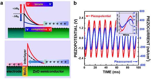 | ||
| Fig. 4 Schematic band diagram and performance of a SPENG with a MoO3 interlayer. (a) (Top) Energy band diagram of the Schottky contact with the presence of a piezopotential at the MS interface. When a tensile strain is applied on the top side, positively charged immobile ions generated by the piezoelectric effect at the interface increase the local Schottky barrier height, while negatively charged non-mobile ions reduce the Schottky barrier height with a compressive strain applied on the top side. (Bottom) Energy band diagram of the MS contact after the insertion of the MoO3 interlayer acting as an efficient electron transport barrier due to its large work function and deep conduction band minimum. (b) The piezoelectric output potential and current simultaneously measured from a SPENG consisting of functionalized 25 mM Li-doped ZnO NWs and the MoO3 interlayer. The inset is the enlarged view of output signals. | ||
To extend the practical piezoelectric function of a ZnO NW, it is highly required to create new viable applications in self-powered electronic devices that can not only preserve advantageous intrinsic piezoelectric potentials but also circumvent the low output current limits, which is another emerging issue to be addressed. To this end, we demonstrate, for the first time, that the optimized SPENG is powerful enough and suitable to drive electrophoretic ink displays, based on a voltage-drive system, which have favorable power consumption characteristics without the need of a constant current supply, and the power to not only maintain text or images, but to turn a page or change it as shown in Fig. 5. In order to operate electrophoretic ink displays, we designed a voltage doubling circuit and achieved the increased output rectified voltage of up to ∼7 V (Fig. 5c). When only the switches numbered ‘1’ are on, the four 1 μF capacitors are charged by the SPENG and then the stored charges are released to power the displays by connecting the four charged capacitors in series once the switches numbered ‘2’ and ‘3’ are turned on subsequently after the switches numbered ‘1’ are turned off.20 As shown in Fig. 5a and b, we successively displayed text on devices by sequentially discharging the capacitors. This is the first time that we demonstrate that the enhanced output power of a SPENG is sufficient to drive commercial electrophoretic displays.
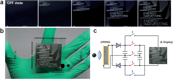 | ||
| Fig. 5 Self-powered electrophoretic displays. (a) Photographs of text displayed on the device after sequentially discharging the capacitors. (b) A photograph of electrophoretic ink displays powered by a SPENG. (c) Schematic diagram of the voltage doubling and charge storage circuit. | ||
In summary, we demonstrate simple and effective approaches to improve the efficiency of piezoelectric energy harvesting through suppressing the undesirable screening effect of the free carriers by a combination of doping and surface modification schemes. Moreover, the performance of a SPENG is further enhanced and maximized by the incorporation of a MoO3 interlayer, which increases an interfacial energy barrier and effectively obstructs free carriers from passing through the interface causing leakage current. The output voltage and current of an optimized SPENG are drastically improved by over 48 and 50 times compared to those of a SPENG based on undoped ZnO NWs, respectively. Furthermore, we demonstrate that output power of our SPENG is sufficient to drive electrophoretic displays. This approach is expected to be an attractive potential strategy, providing the high possibility for realizing multi-functional, self-powered devices with high performances.
Methods
Growth of vertically well-aligned Li-doped ZnO NW arrays for the SPENG
In order to obtain ZnO NWs with different carrier concentrations, Li-doped ZnO NWs were grown on p-type Si substrates with a 50 nm thick ZnO seed layer as catalysts in an aqueous solution containing a 100 ml solution of 25 mM zinc nitrate hexahydrate and a 300 ml solution of 25 mM hexamethylenetetramine by adding a 200 ml solution of 12.5, 25, 50, 100 mM lithium nitrate, respectively, at 85 °C. A ZnO seed layer with a highly oriented columnar structure was deposited at 450 °C by an inductively coupled RF plasma sputtering system using a ZnO ceramic target (99.999%, Kojundo).Surface functionalization of ZnO NWs via oleic acid
In order to modify the surface of ZnO NWs, we performed the functionalization with oleic acid molecules through the carboxylic acid group on the basis of previously reported results that the carboxylic acids are the most common anchoring groups on the surfaces of metal oxides. Furthermore, the surface modification of ZnO nanostructures with carboxylic acids has been also reported. However, from the fact that ZnO is easily damaged during the reactions with carboxylic acids in aqueous solutions, several different organic molecules including the carboxylic acid group have been examined. In this work, we focus our discussion on SPENGs based on ZnO NWs functionalized with the oleic acid molecule by immersion in a 2 ml dichloromethane solution containing 5.8 mg oleic acid for 30 h because it is revealed that ZnO is stable during the reactions with carboxylic acids compared to different organic molecules and solutions. After functionalization, NWs were washed with methanol thoroughly to remove residue oleic acid.Electrophoretic ink display
The bottom Al electrodes were patterned on a glass substrate by a conventional photolithography process. Electrophoretic ink capsules mixed with resin were printed on indium tin oxide (ITO) coated PET (polyethylene terephthalate) substrate, which was laminated on the glass substrate. The ink in the capsule is physically moved by an electrostatic field generated by the Al-electrodes and ITO film and displays a black and white image. The driving voltages of the ink cell depend on device structures such as the cell gap, the thickness of the resin and the adhesion quality of the lamination process. The device proposed in this work has shown 5–7 V of driving voltages.References
- S. Xu, et al. Self-powered nanowire devices, Nat. Nanotechnol., 2010, 5, 366–373 CrossRef CAS.
- S. D. Oosterhout, et al. The effect of three-dimensional morphology on the efficiency of hybrid polymer solar cells, Nat. Mater., 2009, 8, 818–824 CrossRef CAS.
- J. A. Turner, A realizable renewable energy future, Science, 1999, 285, 687–689 CrossRef CAS.
- Special issue on Sustainability and Energy, Science, 2007, 315, 781–813 Search PubMed.
- J. H. Brown, et al. Energetic limits to economic growth, BioScience, 2011, 61, 19–26 CrossRef.
- Z. L. Wang and J. H. Song, Piezoelectric nanogenerators based on zinc oxide nanowire arrays, Science, 2006, 312, 242–246 CrossRef CAS.
- M. Law, L. E. Greene, J. C. Johnson, R. Saykally and P. Yang, Nanowire dye-sensitized solar cells, Nat. Mater., 2005, 4, 455–459 CrossRef CAS.
- G. E. Jabbour and D. Doderer, Quantum dot solar cells: the best of both worlds, Nat. Photonics, 2010, 4, 604–605 CrossRef CAS.
- P. Yang, R. Yan and M. Fardy, Semiconductor nanowire: what's next?, Nano Lett., 2010, 10, 1529–1536 CrossRef CAS.
- Z. L. Wang, ZnO nanowire and nanobelt platform for nanotechnology, Mater. Sci. Eng., R, 2009, 64, 33–71 CrossRef.
- Y. Hu, et al. Self-powered system with wireless data transmission, Nano Lett., 2011, 11, 2572–2577 CrossRef CAS.
- G. Romano, et al., Piezoelectric potential in vertically aligned nanowires for high output nanogenerators, Nanotechnology, 2011, 22, 465401 CrossRef.
- S. Cha, et al. Sound-driven piezoelectric nanowire-based nanogenerators, Adv. Mater., 2010, 22, 4726–4730 CrossRef CAS.
- X. Wang, J. Song, J. Liu and Z. L. Wang, Direct-current nanogenerator driven by ultrasonic waves, Science, 2007, 316, 102–105 CrossRef CAS.
- R. Yang, Y. Qin, L. Dai and Z. L. Wang, Power generation with laterally packaged piezoelectric fine wires, Nat. Nanotechnol., 2009, 4, 34–39 CrossRef CAS.
- M.-Y. Choi, et al. Mechanically powered transparent flexible charge-generating nanodevices with piezoelectric ZnO nanorods, Adv. Mater., 2009, 21, 2185–2189 CrossRef CAS.
- B. Kumar, et al. Controlled growth of semiconducting nanowire, nanowall, and hybrid nanostructures on graphene for piezoelectric nanogenerators, ACS Nano, 2011, 5, 4197–4204 CrossRef CAS.
- S. Xu, B. J. Hansen and Z. L. Wang, Piezoelectri-nanowire-enabled power source for driving wireless microelectronics, Nat. Commun., 2010, 1, 93 CrossRef.
- J. Hu, A. P. Suryavanshi, K. Yum, M. F. Yu and Z. Y. Wang, Voltage generation from individual BaTiO3 nanowires under periodic tensile mechanical load, Nano Lett., 2007, 7, 2966–2969 CrossRef.
- S. Cha, et al. Porous PVDF as effective sonic wave driven nanogenerators, Nano Lett., 2011, 11, 5142–5147 CrossRef CAS.
- J. Lee, et al. p-Type conduction characteristics of lithium-doped ZnO nanowires, Adv. Mater., 2011, 23, 4183–4187 CrossRef CAS.
- M. G. Wardle, J. P. Goss and P. R. Briddon, Theory of Li in ZnO: a limitation for Li-base p-type doping, Phys. Rev. B: Condens. Matter Mater. Phys., 2005, 71, 155205 CrossRef.
- C. Rauch, et al. Lithium related deep and shallow acceptors in Li-doped ZnO nanocrystals, J. Appl. Phys., 2010, 107, 024311 CrossRef.
- L. Wang and N. C. Giles, Determination of the ionization energy of nitrogen acceptors in zinc oxide using photoluminescence spectroscopy, Appl. Phys. Lett., 2004, 84, 3049–3051 CrossRef CAS.
- J. I. Sohn, et al. The influence of surface chemical dynamics on electrical and optical properties of ZnO nanowire field effect transistors, Nanotechnology, 2009, 20, 505202 CrossRef.
- D. Liu, et al. Surface functionalization of ZnO nanotetrapods with photoactive and electroactive organic monolayers, Langmuir, 2008, 24, 5052–5059 CrossRef CAS.
- P. R. Brown, et al. Improved current extraction from ZnO/PbS quantum dot heterojunction photovoltaics using a MoO3 interfacial layer, Nano Lett., 2011, 11, 2955–2961 CrossRef CAS.
- J. Gao, et al. n-Type transition metal oxide as a hole extraction layer in PbS quantum dot solar cells, Nano Lett., 2011, 11, 3263–3266 CrossRef CAS.
Footnote |
| † Electronic supplementary information (ESI) available. See DOI: 10.1039/c2ee23404a |
| This journal is © The Royal Society of Chemistry 2013 |