Pore size modulation in electrochemically etched macroporous p-type silicon monitored by FFT impedance spectroscopy and Raman scattering†
Enrique
Quiroga-González
a,
Jürgen
Carstensen
a,
Colm
Glynn
b,
Colm
O'Dwyer
bc and
Helmut
Föll
*a
aInstitute for Materials Science, Christian-Albrechts-University of Kiel, Germany. E-mail: equiroga@ieee.org; jc@tf.uni-kiel.de; hf@tf.uni-kiel.de; Fax: +49(431)8806178; Tel: +49(431)8806176
bDepartment of Chemistry, University College Cork, Ireland. E-mail: colm.j.glynn@gmail.com; c.odwyer@ucc.ie
cMicro & Nanoelectronics centre, Tyndal National Institute, Cork, Ireland
First published on 30th October 2013
Abstract
The understanding of the mechanisms of macropore formation in p-type Si with respect to modulation of the pore diameter is still in its infancy. In the present work, macropores with significantly modulated diameters have been produced electrochemically in p-type Si. The effect of the current density and the amount of surfactant in the etching solution are shown to influence the modulation in pore diameter and morphology. Data obtained during the etching process by in situ FFT impedance spectroscopy correlate the pore diameter variation with certain time constants found in the kinetics of the dissolution process. Raman scattering and electron microscopy confirm the mesoscopic structure and roughening of the pore walls. Spectroscopic and microscopic methods confirm that the pore wall morphology is correlated with the conditions of pore modulation.
1. Introduction
Macroporous Si with modulated pore diameters is of importance for a variety of applications. It supplies the base material for the preparation of self-standing Si microwires and Si microparticles,1–4 photonic crystals,5–9 and micropumps and membranes.10–12 Additionally, it has been used in solar cell applications,13–16 and as a template for the preparation of metal wires or tubes.17,18 Most of the reports on macroporous Si with modulated diameters deal with n-type Si. Since the discovery of the etching process to make macroporous Si using n-type material and backside illumination in 1990,19 considerable work has been dedicated to controlling and varying the structure and morphology of macroporous n-type Si. The etching mechanism has been understood, at least under standard etching conditions,20–22 and there are also several publications detailing pore diameter modulations, including some reviews.23–25 In strong contrast, reports on pore diameter modulation in p-type Si are rather scarce.1–3,26Modulation of pore diameters in n-type Si under standard etching conditions (i.e. using low HF concentration of up to 4 wt%) can be easily obtained (and understood) by modulating the current density,22 taking into account the process of self-organization encountered27,28 during etching. The so-called Lehmann model20 is applicable in suitable ranges of the parameter space. The model assumes that for the etching process the current is mainly photocurrent, and that the current density at the pore tips is determined by the maximum current density jPS found in the current–voltage characteristics of the system obtained under saturation photo-current conditions, with limited contribution from carrier diffusion along the pore–wall interface. The current density jPS is constant under the given conditions of temperature, etchant concentration, and depth. As the current density at the pore tips is constant, varying the total current i can control the pore diameters d since π(d/2)2jPS = i. Good n-Si macropore formation implies that at the vicinity of the pore tip the pore walls are almost completely passivated, i.e. that a full SCR (space-charge region) is formed, but this is not always assured, however. The dissolution process induces charged surface states, which may reduce the width of the SCR and thus the focusing effect of the SCR, allowing thinning or over-etching of the pore walls. Since pore diameter modulations also modulate the speed of the pore growth into the bulk, the passivation kinetics should also be considered. Faster pore growth with increasing depth, for example, requires electrolyte additives (surfactants) that reduce dissolution kinetics by improved passivation.
In p-type Si, the modulation of the pore diameter is more complicated. In this case, the etching process is generally omnidirectional owing to the high hole concentration and faster hole mobility at the interface, and lateral pore growth is severely limited by the SCR between pores.29–31 Since the availability of electronic holes necessary for the etching is much higher in p-type silicon than in n-type silicon, a selective passivation of pore walls is much more difficult to achieve. This necessary selective passivation is strongly influenced by several factors: (i) the crystal anisotropy, for example, {100} oriented pore walls are more susceptible to over-etching than {111} pore walls; (ii) overlapping SCR, enforced by pre-structured nucleation sites with suitable geometry; (iii) strongly surface-passivating electrolytes; (iv) a large curvature around the pore tips, leading to a large electrical field at the pore tip. Experimentally it has been found that if current densities much lower than jPS are used, it is possible to reduce the pore diameters by decreasing the current1 during etching, allowing pore diameter modulation. Additionally, it has been reported that electrolyte additives like polyethyleneglycol (PEG) enhance attempted diameter modulations by improving the passivation of the pore walls.26
In this paper, the effect of the current and PEG additions on the pore diameter modulation of macropores in p-type Si is studied. Additionally, Fast Fourier Transformation Impedance Spectroscopy (FFT-IS), SEM microscopy and Raman scattering spectroscopy are used to elucidate details of the microstructure of the modulated macropores and the mesostructure of their pore walls.
2. Experimental details
Electrochemical etching of pores was performed on p-type Si wafers with resistivity (15–25) Ω cm. Previous to the experiments a square array of inverted pyramids with basis size of 2.2 μm × 2.2 μm was formed on the wafers by contact lithography, reactive ion etching, and chemical etching in a KOH solution. The distance from center to center of the pyramids was 3 μm in the 〈100〉 directions. Further details on the patterning are given in ref. 1. Fig. 1 shows an example of the top view of the pores etched from these substrates.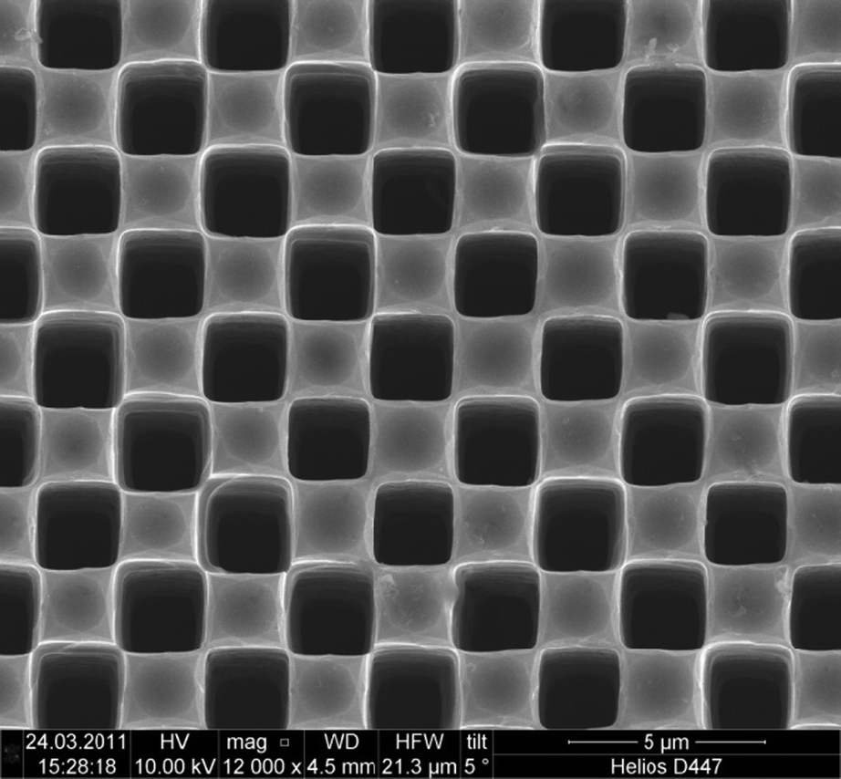 | ||
| Fig. 1 Top view of a typical macroporous sample prepared for this work. The distance from center to center of the pores is 3 μm. | ||
The pore etching experiments were performed galvanostatically, using the current profile of Fig. 2a. The current profile consists of sections of two different constant currents (high and low). The “high current” was 20, 30, or 35 mA, while the “low current” was 3 mA for all the experiments. The etched area (surface area of Si in contact with the electrolyte) was 0.78 cm2. The high currents produce sections of wide pore diameter, while the low currents produce sections of narrow pore diameter, with diameters W and N, respectively. A schematic of the pores is shown in Fig. 2b. The etching electrolyte was composed of 220 mL N,N′-dimethylformamide (DMF) and 22 mL HF. Additionally 0, 1, or 2 g polyethyleneglycol 3600 (PEG, 3600 g mol−1) were added to the etchant. The temperature for the experiments was kept constant at 20 °C. The electrolyte was pumped through the etching cell (with capacity of 7 mL) at a rate of 600 mL min−1 from a temperature controlled container that has a capacity of 400 mL. This allows a stable temperature in the etching cell, and avoids problems like electrolyte depletion. The reference electrode was positioned close to the samples to be etched (at around 2 mm distance), to keep the contribution of the electrolyte in the voltage and impedance measurements as small as possible. A simple schematic of the etching system can be found in ref. 32 and 33, with the difference that for the present experiments no backside illumination was needed. A list of the produced samples is shown in Table 1. In etching experiments employing 35 mA currents and 2 g PEG, the macropores were destroyed after reaching certain depths; the samples produced under these extreme etching conditions were not evaluated for the present work.
 | ||
| Fig. 2 (a) Current profile used for the electrochemical etching experiments. The current alternated between high current (20, 30, or 35 mA) and low current (3 mA). (b) Schematic of a pore, indicating the wide and narrow pore sections, with diameters W and N respectively; these sections are obtained with high and low currents respectively. | ||
| Sample | High current [mA] | Amount PEG [g] |
|---|---|---|
| 20_0 | 20 | 0 |
| 20_1 | 20 | 1 |
| 20_2 | 20 | 2 |
| 30_0 | 30 | 0 |
| 30_1 | 30 | 1 |
| 30_2 | 30 | 2 |
| 35_0 | 35 | 0 |
| 35_1 | 35 | 1 |
For the electrochemical etching experiments and FFT-IS measurements, a fully integrated laboratory etching system of ET&TE GmbH was used. FFT-IS spectra at 24 frequencies in a range from 5 Hz to 20 kHz were recorded in situ every 2 s. Microstructural characterization was done using an SEM microscope Helios D477 from FEI.
Raman scattering spectroscopy was conducted using a Horiba Jobin-Yvon Dilor XY Labram spectrometer with an Olympus BX40 confocal microscope. The excitation source was a 532 nm solid state 100 mW laser (filtered). The Raman spectra were collected using a Peltier-cooled CCD detector.
3. Results
3.1. Pore structure
Fig. 3 shows samples etched without PEG for the three “high currents”. The modulation of the pore diameters is observed in all samples. This confirms the idea that by varying the current densities one can vary the pore diameters, even in p-type Si, in contrast to previous reports, where an increase in the etching rate but no modification of the pore diameter30,31 is observed. At first glance, one can see that both, the length and the width of the pores are affected by modulation of the current density. | ||
| Fig. 3 Micrographs of pores etched with no PEG and (a) 20, (b) 30, and (c) 35 mA. The width of all the images is the same (12.7 μm), for a better comparison. The pieces in the pores of the sample etched at 35 mA are simply pieces of Si, due to an imperfect cleavage (the samples were cleaved for the observations). | ||
Examples for visualizing the effect of PEG on the pore modulation are shown in Fig. 4. This figure shows SEM micrographs of pores prepared using 20 mA “high currents” and different levels of PEG.
 | ||
| Fig. 4 Micrographs of pores etched with 20 mA and (a) 0, (b) 1, and (c) 2 g PEG. The width of all the images is the same (12.7 μm), for a better comparison. | ||
By visual inspection it is possible to identify a good contrast between “narrow” (N) and “wide” (W) pore regions in all the samples, but it is clear that it is enhanced through the use of PEG. Shallower pores are typically found when using higher quantities of PEG additive. Plots of the diameters N and W as a function of the PEG concentration for the different “high currents” are shown in Fig. 5. N and W vary continuously with the amount of PEG; the diameters mainly increase with a greater amount of PEG, except for N in the samples obtained with 20 mA “high current”. In this last case N decreases by using more PEG.
 | ||
| Fig. 5 Pore diameters at the (a) N sections and (b) W sections for the samples prepared with high currents equal to 20, 30, and 35 mA. | ||
A plot of the etching rates for etching the W sections prior to the development of the narrowing regions N is shown in Fig. 6. The etching rate increases with greater etching current, but the rate is retarded when greater amounts of PEG are added to the etching solution.
 | ||
| Fig. 6 Etching rate when preparing the W sections with high currents equal to 20, 30, and 35 mA, before the first narrowing. | ||
Fig. 7 shows high magnification SEM images of the W sections obtained at the different currents without PEG. Clearly the roughness (meso-structure) increases with larger applied currents for a given pore diameter. On the other hand, the degree of pore wall texture becomes finer (the features are smaller, but denser) when increasing the amount of PEG. Fig. 8 shows an example of this effect for pores prepared with 30 mA without PEG and also with 2 g PEG. The same effect is found for the samples prepared with a high current of 20 mA, but it is different for the ones prepared with 35 mA. The addition of 1 g of PEG at the highest etching current of 35 mA causes some shallow cavity formation on the pore wall.
 | ||
| Fig. 7 Micrographs of the pore wall surfaces at wide sections of samples etched without PEG and (a) 20 and (b) 35 mA. The level of roughness increases when increasing the etching current. | ||
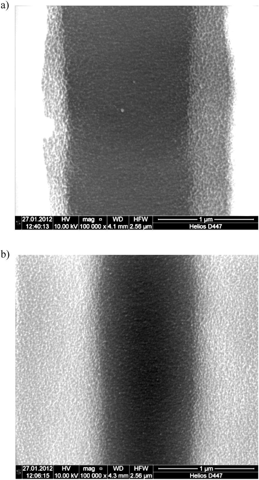 | ||
| Fig. 8 Micrographs of the surface of the pore walls at wide sections of samples etched with 30 mA current and (a) no PEG, (b) 2 g PEG. The roughness gets finer (smaller and denser features) by adding PEG. | ||
SEM images in high magnification of all the samples are provided as ESI† (S1). All these tendencies are represented graphically in Fig. 9, where a qualitative plot of the roughness versus the amount of PEG is shown for every high current, determined through visual inspection analysis of the microscopy data.
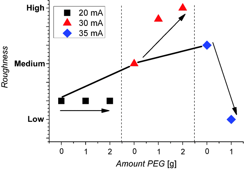 | ||
| Fig. 9 Qualitative plot of the roughness versus the amount of PEG is shown for every high current. The lines are an aid for a better visualization. | ||
To get a quantitative measure of the roughness and texture change as a function of the PEG passivation and its influence on pore wall etch rates, Raman scattering was used.
Raman scattering is commonly used for estimating Si crystallite sizes, and in the case of roughness it is a very powerful technique for probing texture effects on phonon scattering at roughened interfaces and crystalline boundaries.34–36 Typically, the width and asymmetry caused by different phonon scattering and dispersion are most evident in the transverse optical phonon (TO) mode,37–40 which is centered at ∼520 cm−1 for crystalline Si. As the crystallite size associated with the meso-scale roughness or with the micro-crystalline Si decreases, the Raman shift and peak width increase and the line-shape becomes asymmetric with an extended tail at lower energies for phonon confinement effects.41–43 A typical Raman spectrum of the samples described above is shown in Fig. 10. As can be seen in Fig. 10, the TO peak at ∼520 cm−1 and the two phonon 2TO mode at ∼960 cm−1 can be detected, as well as a peak at ∼300 cm−1, which is the two phonon 2TA mode of Si. The intensity of this last peak is two orders of magnitude smaller than the TO peak, as is the case of crystalline Si. This mode would be enhanced just if an amorphous Si phase is present, where also LA phonons are enabled;44 thus the samples are crystalline and any passivation or randomization/amorphization of the effective surface by roughening is negligible, i.e. the rough features on pore walls are remnant Si left from etching, and not individual crystallites.
 | ||
| Fig. 10 Typical Raman spectrum of the studied samples. The common Raman peaks of crystalline Si can be identified. | ||
In a relatively recent report, the asymmetry of the TO peak has been used for determining the crystallite sizes;45 this method is independent of the absolute height and width of the Raman peak. For the present study, as the differences in asymmetry between samples are in the same range of the error upon considering the center of the peak, this method is not considered. The full width at half maximum of the peaks (FWHM) was considered for this study. In Fig. 11 a plot of the FWHM versus the amount of PEG used for the etching, for each of the high currents, is shown. When comparing the samples prepared with no PEG, one can see that the FWHM widens at increasing the etching current.
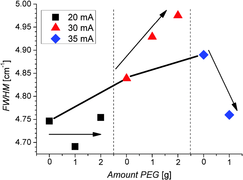 | ||
| Fig. 11 FWHM of the TO Raman peak of the different samples, versus the amount of PEG used for the etching, for the different etching currents. The lines are an aid for a better visualization. | ||
On the other hand, the FWHM exhibits different tendencies depending on the applied current, when increasing the amount of PEG (see the arrows in the figure). These are the same tendencies observed in Fig. 9, for the qualitative analysis of the roughness of the samples (nanoscale features lining the inner walls of the macropores). Nanoscale features like the described roughness typically tend to result in some degree of phonon confinement, but also contribute to asymmetry in the line shape from surface scattering effects. In practice, one observes changes in the Raman spectrum related to size effects via phonon confinement just when the crystallites are smaller than 100 nm (wavevector dependent); it is thus very plausible that the changes in FWHM described in Fig. 11 are related to the roughness of the pore walls which result in diffusive rather than specular phonon scattering46 at the rough interface, corroborating the qualitative analysis of Fig. 9. The roughness increases with the applied current when no PEG is used, and the effect of PEG on the roughness varies with applied current.
3.2. Pore structure
FFT-IS is a powerful technique for the electrochemical characterization and physicochemical modeling of electrochemical systems.47–53 This technique can be applied in situ, since it has the capability of measuring an impedance spectrum in very short times, usually for durations <1 s. With the aid of FFT-IS major insights into the pore etching process have already been obtained, especially for n-type Si etched with backside illumination50,54 or n-type InP.55,56 Additionally, the results on p-type Si are encouraging.26,57The data obtained from the impedance measurements during the electrochemical etching of the samples can be satisfactorily fitted with an equivalent circuit model containing a series resistor (Rs) and 3 time constants (τ1, τ2, and τ3) that are coupled with the resistors R1, R2, and R3. This model agrees with the previous reports on electrochemical etching of macropores in p-type Si.26,57 The impedance Z of the model can be represented mathematically by
 | (1) |
An impedance spectrum was obtained every 2 s during the etching. Every spectrum obtained was fitted to eqn (1) and the parameters were extracted in real time. An example of the fit is shown in Fig. 12. One of such fitted spectrum was obtained every 6 s during etching. The results of the fit parameters were plotted as a function of time. Fig. 13 shows the values of the time constants for the sample etched with 30 mA high current and 2 g of the PEG additive. Here, the parameters that predominantly follow the form of the current profile (see Fig. 2a) are the time constants. The other parameters do not show an apparent correlation.
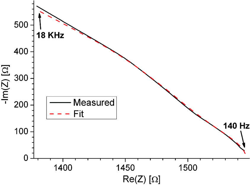 | ||
| Fig. 12 Example of fit of impedance data (sample etched with 20 mA high current and 1 g PEG). One such fitted spectrum was obtained every 6 s during etching for all the samples. | ||
 | ||
| Fig. 13 Time constants τ1, τ2, and τ3 of the etching process for the sample prepared with 30 mA high current and 2 g PEG. The blue line indicates the center of the time at “low current”. | ||
As in ref. 26, where PEG was used as an additive, in the present work it is considered that τ1 is related to the etching at the pore tip, which is nominally the fastest process assuming that the electrochemical reaction dominates over carrier diffusion at the interface since this effect is insignificant for p-type Si where holes are majority carriers with a large bulk concentration. τ2 is considered to be related to the dissolution of the pore walls, which can occur through hole supply at the wall interface (from p-type silicon). Since holes are readily available in p-silicon, carrier diffusion is less dominant and the etching current at any point away from the tip is a function of the radius of curvature of the pore walls. As this radius of curvature is much larger than the apex of the pore tip, the etching process at the walls is comparatively slower. For τ3 it has been observed that it varies with the amount of PEG, as depicted in Fig. 14, where the value of τ3 is plotted versus the amount of PEG, for every high current. The origin of τ3 can be ascribed to the diffusion of the electrolyte during the etching process, and more directly to the diameters of the pores, as will become clear in the section for Discussion. In ref. 26 it was not clear which was the origin of this time constant, but it was related to certain “transitions” of carriers from the pore tips to the PEG-passivated walls. That model fits good with the practical observations when using high currents in the range of 20 mA, but not with the data obtained using higher currents.
 | ||
| Fig. 14 Time constant τ3 for the samples prepared with high currents equal to 20, 30, and 35 mA. The values were taken at the middle of the time for etching the narrow sections. | ||
4. Discussion
4.1. Pore structure
 | ||
| Fig. 15 Pore diameters at the N and W sections of the samples prepared with “high currents” equal to 20, 30, and 35 mA with no PEG. | ||
It can be seen from this figure that W increases when going from 20 to 30 mA high current, but decreases with a further increase of the current to 35 mA. This can be explained as follows: at currents up to 30 mA the etching of Si occurs with the hole provided from the bulk at the pore tip and at the walls. The highest current of 35 mA corresponds to the initial peak current (density) corresponding to electropolishing, current densities larger than jPS. For this process, tunneling of holes through the (thin) space charge region occurs in addition to diffusion. The tunneling process occurs preferentially at the pore tips, due to the narrower space charge region caused by the high tip curvature. Thinner and longer pores propagate when the majority of the charge transport is localized at the pore tip,58,59 and the overall shape of the pore is influenced by the rate of reaction at the pore tip versus that occuring at the pore walls. In the present case the etching rate in the axial direction increases when increasing the high currents to 35 mA (see Fig. 6), while the pores become thinner when etching with this current.
The diameter N is also affected by the “high currents”, as seen in Fig. 15. This is remarkable since N could be expected to be the same for all the samples prepared with the same amount of PEG, independently of the intensity of the “high current”, since these sections are produced during the application of the always identical “low current”. Nevertheless, as the process for over-etching the W sections is relatively isotropic, the already etched N sections would also get over-etched at this stage. For this reason, the pore widths of the N sections follow a similar trend as the W sections when increasing the high currents.
The dependency of the pore diameters W on PEG additions can be observed in Fig. 5b. With additions of PEG the pore walls and the pore tip become more passivated, which reduces the etching rate at the pore tip and makes the etching more isotropic, i.e. lateral growth and depth growth rates are less different, thus the pores become wider. For the pore diameters N the same effect can be observed, except when etching with 20 mA current. For this current the over-etched region may be minimum (there is no constraint of availability of holes at the pore tips for this low current), and it may be even smaller when increasing the amount of PEG, since the pore walls may be better passivated. In this way, the N sections are less over-etched, and thus, they are thinner.
The increasing roughness of the samples by increasing the high current or the amount of PEG can explain the level of passivation at the pore tips, which increases/reduces the chance of modulating pores. PEG offers some degree of passivation, but clearly does not eliminate charge transfer completely. PEG could potentially retard the rate of etching for uniform PEG coverage, or in the case of uneven coverage of the pore wall, only allow etching at uncoated sites which still amounts to the lowest rate of etching and thus current. A clear correlation between the ability of a PEG containing electrolyte to allow for significant pore diameter modulation and the meso-structure of the surface of the pore walls is found at least for not too high current densities: the higher the PEG content, the finer is the meso-structure at the pore walls and the more pronounced is the pore diameter modulation induced by steps in the etching current density. Just in the samples prepared with 35 mA the roughness decreases when increasing the amount of PEG. A current of 35 mA may approach the limit of electropolishing, which may be enhanced with PEG. Overall, given the high density of varied crystallographic surface terminations on the rough pore walls, as opposed to the nominal {100} planes associated with the square profile of the walls into the bulk of the semiconductor, the PEG passivation appears to be effective by coating multifaceted or rough semiconductor surfaces.
4.2. Indication of diameter modulation by FFT-IS
As can be observed from Fig. 14, there is a strong influence of the amount of PEG in the etching solution on the value of the time constant τ3 of the etching process, calculated from FFT-IS data. The dependency is direct (a correlation with positive slope is observed), except for the samples prepared using a high current of 20 mA. A similar tendency is exhibited by the N sections of the pores when increasing the amount of PEG (see the tendencies of N in Fig. 5a). This may be an indication that τ3 depends on the diameter of the narrow sections. A plot combining the data of Fig. 5a and 11 is shown in Fig. 16. It can be seen from the figure that τ3 can have a direct (30 and 35 mA) or inverse (20 mA) relation with the amount of PEG (indicated with arrows), but it has a direct relation with the diameter of N (indicated with the dashed line). An increment in the diameter of N implies an enhancement or constraint for the diffusion of the etching solution. Impedance spectroscopy correlated with the microscopy measurements leads to the possibility that τ3 is likely related to the time constant of the diffusion process. This is very plausible, since this time constant is two orders of magnitude slower than any of the other two time constants, which are related to electron transfer processes. τ3 could be used for estimating the diameter of narrowing pores during their diameter modulation. | ||
| Fig. 16 Dependency of the time constant τ3 on the pore diameter at the narrow sections. For the samples prepared with high currents equal to 20, 30, and 35 mA. The lines are an aid for a better visualization. | ||
5. Conclusion
Macropores with modulated pore diameters have been successfully produced electrochemically in p-type Si. Polyethyleneglycol (PEG) has been used as an additive for the etchant in different amounts.The etching current has also a direct influence on the pore diameter. At low and moderate currents a direct dissolution of Si occurs, given the electron holes at the pore tip and at the walls; in this current range the pores get wider with increments in current. At currents close to the range of electropolishing, tunneling of carriers occurs, which is preferential at the pore tips; this makes the pores narrower again.
The diameter of the narrow and the wide pore sections varies continuously with the amount of PEG. The diameters mainly increase with a greater amount of PEG additive, except for the narrow pore sections where the over-etching produced during the production of the wide sections is minimum (when moderate currents are used). The pore walls and the pore tip become effectively passivated with PEG. This passivation reduces the localized etching rate at the pore tip and makes the etching more isotropic (the walls are consumed more). The roughness of the pore walls, measured by monitoring the variation in phonon scattering at the roughened surface, correlates well with the effect of passivation on the etching mechanism, and consequently, with the ability to modulate pores and modify the pore wall texture.
Different time constants of processes occurring during etching can be calculated from FFT impedance spectroscopy data. In this work a correlation of one of the time constants with the diameter of the narrow sections was observed. It may be possible to detect the variations in diameter of the narrow sections by FFT impedance spectroscopy.
Notes and references
- E. Quiroga-González, E. Ossei-Wusu, J. Carstensen and H. Föll, J. Electrochem. Soc., 2011, 158, E119 CrossRef PubMed.
- C. M. van Kats, P. M. Johnson, J. E. A. M. van den Meerakker and A. van Blaaderen, Langmuir, 2004, 20, 11201 CrossRef CAS PubMed.
- H. Föll, E. Quiroga-González, E. Ossei-Wusu, J. Carstensen and M. Amirmaleki, in Conference proceedings of the 2nd International Conference on Nanotechnologies and Biomedical Engineering, Chisinau, Republic of Moldova, 2013.
- H. Föll, J. Carstensen, E. Ossei-Wusu, A. Cojocaru, E. Quiroga-González and G. Neumann, J. Electrochem. Soc., 2011, 158, A580 CrossRef PubMed.
- S. Matthias, F. Mueller, J. Schilling and U. Gösele, Appl. Phys. A: Mater. Sci. Process., 2005, 80, 1391 CrossRef CAS.
- S. Matthias, F. Müller, C. Jamois, R. B. Wehrspohn and U. Gösele, Adv. Mater., 2004, 16, 2166 CrossRef CAS.
- A. Birner, R. Wehrspohn, F. Müller, U. Gösele and K. Busch, Adv. Mater., 2001, 13, 377 CrossRef CAS.
- J. Schilling, F. Müller, S. Matthias, R. B. Wehrspohn, U. Gösele and K. Busch, Appl. Phys. Lett., 2001, 78, 1180 CrossRef CAS.
- F. Müller, A. Birner, U. Gösele, V. Lehmann, S. Ottow and H. Föll, J. Porous Mater., 2000, 7, 201 CrossRef.
- F. Müller, A. Birner, J. Schilling, U. Gösele, C. Kettner and P. Hänggi, Phys. Status Solidi A, 2000, 182, 585 CrossRef.
- S. Matthias and F. Müller, Nature, 2003, 424, 53 CrossRef CAS PubMed.
- K. Mathwig, M. Geilhufe, F. Müller and U. Gösele, J. Micromech. Microeng., 2011, 21, 035015 CrossRef.
- V. Dapauw, I. Gordon, G. Beaucarne, J. Poortmans, R. Mertens and J.-P. Celis, Mater. Sci. Eng., B, 2009, 159–160, 286 CrossRef PubMed.
- K.-Q. Peng, X. Wang, X. Wu and S.-T. Lee, Appl. Phys. Lett., 2009, 95, 143119 CrossRef.
- C. Lévy-Clément, S. Lust, S. Bastide, Q. N. Le and D. Sarti, Phys. Status Solidi A, 2003, 197, 27 CrossRef.
- V. Dapauw, O. Richard, H. Bender, I. Gordon, G. Beaucarne, J. Poortmans, R. Mertens and J.-P. Celis, Thin Solid Films, 2008, 516, 6934 CrossRef PubMed.
- K. Kobayashi, F. A. Harraz, S. Izuo, T. Sakka and Y. H. Ogata, J. Electrochem. Soc., 2006, 153, C218 CrossRef CAS PubMed.
- X. Badel, J. Linnros, P. Kleimann, B. Norlin, E. Koskiahde, K. Valpas, S. Nenonen, C. S. Petersson and C. Fröjdh, IEEE Trans. Nucl. Sci., 2004, 51, 1001 CrossRef CAS.
- V. Lehmann and H. Föll, J. Electrochem. Soc., 1990, 137, 653 CrossRef CAS PubMed.
- V. Lehmann, J. Electrochem. Soc., 1993, 140, 2836 CrossRef CAS PubMed.
- V. Lehmann and U. Gösele, Mater. Res. Soc. Symp. Proc., 1993, 283, 27 CrossRef CAS PubMed.
- V. Lehmann and U. Grüning, Thin Solid Films, 1997, 297, 13 CrossRef CAS.
- S. Matthias, F. Müller, J. Schilling and U. Gösele, Appl. Phys. A: Mater. Sci. Process., 2005, 80, 1391 CrossRef CAS.
- A. Langner, F. Müller and U. Gösele, in Molecular- and nano-tubes, ed. O. Hayden, K. Nielsch and D. Wang, Springer, New York, 2011, p. 431 Search PubMed.
- H. Föll, M. Leisner, A. Cojocaru and J. Carstensen, Materials, 2010, 3, 3006 CrossRef.
- E. Ossei-Wusu, J. Carstensen, E. Quiroga-González, M. Amirmaleki and H. Föll, ECS J. Solid State Sci. Technol., 2013, 2, P243 CrossRef CAS PubMed.
- A. Cojocaru, J. Carstensen, M. Leisner, H. Föll and I. M. Tiginyanu, Phys. Status Solidi C, 2009, 206, 1533 CrossRef.
- H. Föll, M. Leisner, A. Cojocaru and J. Carstensen, Electrochim. Acta, 2009, 55, 327 CrossRef PubMed.
- V. Lehmann and S. Rönnebeck, J. Electrochem. Soc., 1999, 146, 2968 CrossRef CAS PubMed.
- J. Carstensen, M. Christophersen and H. Föll, Mater. Sci. Eng., B, 2000, 69–70, 23 CrossRef.
- V. Kochergin and H. Föll, Porous semiconductors: Optical properties and applications, Springer, London, 2009 Search PubMed.
- M. Christophersen, J. Carstensen, A. Feuerhake and H. Föll, Mater. Sci. Eng., B, 2000, 69–70, 194 CrossRef.
- M. Christophersen, J. Carstensen, S. Rönnebeck, C. Jäger, W. Jäger and H. Föll, J. Electrochem. Soc., 2001, 148, E267 CrossRef CAS PubMed.
- M. G. Ghossoub, K. V. Valavala, M. Seong, B. Azeredo, K. Hsu, J. S. Sadhu, P. K. Singh and S. Sinha, Nano Lett., 2013, 13, 1564 CAS.
- J. Lim, K. Hippalgaonkar, S. C. Andrews, A. Mujumdar and P. Yang, Nano Lett., 2012, 12, 2475 CrossRef CAS PubMed.
- J. P. Feser, J. S. Sadhu, B. P. Azeredo, K. H. Hsu, J. Ma, J. Kim, M. Seong, N. X. Fang, X. Li, P. M. Ferreira, S. Sinha and D. G. Cahill, J. Appl. Phys., 2012, 112, 114306 CrossRef.
- C. Ossadnik, S. Veprek and I. Gregora, Thin Solid Films, 1999, 337, 148 CrossRef CAS.
- S. V. Gaisler, O. I. Semenova, R. G. Sharafutdinov and B. A. Kolesov, Phys. Solid State, 2004, 46, 1528 CrossRef CAS.
- H. S. Mavi, A. K. Shukla, R. Kumar, S. Rath, B. Joshi and S. S. Islam, Semicond. Sci. Technol., 2006, 21, 1627 CrossRef CAS.
- B. Li, D. Yu and S. L. Zhang, Phys. Rev. B: Condens. Matter Mater. Phys., 1999, 59, 1645 CrossRef CAS.
- S. K. Gupta and P. K. Jha, Solid State Commun., 2009, 149, 1989 CrossRef CAS PubMed.
- K. W. Adu, H. R. Gutiérrez, U. J. Kim and P. C. Eklund, Phys. Rev. B: Condens. Matter Mater. Phys., 2006, 73, 155333 CrossRef.
- I. F. Crowe, M. P. Halsall, O. Hulko, A. P. Knights, R. M. Gwilliam, M. Wojdak and A. J. Kenyon, J. Appl. Phys., 2011, 109, 083534 CrossRef.
- Y. Ma, X. Liao, G. Kong and J. Chu, Sci. China, Ser. A: Math., Phys., Astron., 2000, 43, 414 CrossRef.
- E. Quiroga, W. Bensch, M. Aceves, Z. Yu, J. P. Savy, M. Haeckel and A. Lechner, in IEEE proceedings of the 10th international conference on ultimate integration of silicon, 349, Aachen, Germany, 2009.
- N. Mingo, Phys. Rev. B: Condens. Matter Mater. Phys., 2003, 68, 113308 CrossRef.
- R. J. Schwall, A. M. Bond and D. E. Smith, Anal. Chem., 1977, 49, 1805 CrossRef CAS.
- J. E. Garland, K. A. Assiongbon, C. M. Pettit, S. B. Emery and D. Roy, Electrochim. Acta, 2002, 47, 4113 CrossRef CAS.
- A. Cojocaru, E. Foca, J. Carstensen, M. Leisner, I. M. Tiginyanu and H. Föll, in Proceedings of the 5th international conference on ‘Microelectronics and computer science’, Technical University of Moldova, Chisinau, 2007, vol. 1, p. 133.
- J. Carstensen and H. Föll, ECS Trans., 2009, 25, 11 CrossRef CAS PubMed.
- G. G. Min, Y. Ko, T.-H. Kim, H.-K. Song, S. B. Kim and S.-M. Park, J. Electrochem. Soc., 2011, 158, A1267 CrossRef CAS PubMed.
- K.-M. Nam, D.-H. Shin, N. Jung, M. G. Joo, S.-M. Park and B.-Y. Chang, Anal. Chem., 2013, 85, 2246 CrossRef CAS PubMed.
- E. Quiroga-González, J. Carstensen and H. Föll, Materials, 2013, 6, 626 CrossRef.
- E. Foca, J. Carstensen, G. Popkirov and H. Föll, Phys. Status Solidi A, 2007, 204, 1378 CrossRef CAS.
- M. Leisner, J. Carstensen, A. Cojocaru and H. Föll, Phys. Status Solidi C, 2009, 206, 1566 CrossRef.
- M. Leisner, J. Carstensen, A. Cojocaru and H. Föll, ECS Trans., 2008, 16, 133 CrossRef CAS PubMed.
- E. Ossei-Wusu, J. Carstensen and H. Föll, Nanoscale Res. Lett., 2012, 7, 320 CrossRef PubMed.
- C. O'Dwyer, D. N. Buckley, D. Sutton, M. Serantoni and S. B. Newcomb, J. Electrochem. Soc., 2007, 154, H78 CrossRef CAS PubMed.
- R. Lynch, C. O'Dwyer, N. Quill, S. Nakahara, S. B. Newcomb and D. N. Buckley, J. Electrochem. Soc., 2013, 160, D260 CrossRef CAS PubMed.
Footnote |
| † Electronic supplementary information (ESI) available. See DOI: 10.1039/c3cp53600a |
| This journal is © the Owner Societies 2014 |