Controlling the diffusion profile of electroactive species for selective anodic stripping voltammetry of cadmium at boron-doped diamond electrodes†
Ai
Sugitani
a,
Takeshi
Watanabe
a,
Tribidasari A.
Ivandini
ab,
Tatsuo
Iguchi
c and
Yasuaki
Einaga
*ad
aDepartment of Chemistry, Faculty of Science and Technology, Keio University, 3-14-1 Hiyoshi, Yokohama 223-8522, Japan. E-mail: einaga@chem.keio.ac.jp
bDepartment of Chemistry, Faculty of Mathematics and Science, University of Indonesia, Kampus UI Depok, Jakarta 16424, Indonesia
cDepartment of Mathematics, Faculty of Science and Technology, Keio University, 3-14-1 Hiyoshi, Yokohama 223-8522, Japan
dJST, CREST, 3-14-1 Hiyoshi, Yokohama 223-8522, Japan
First published on 24th October 2012
Abstract
Selective anodic stripping voltammetry of trace metal ions in a mixture solution with another interfering metal was developed based on Fick's law concerning the diffusion profile of interfering metals at the electrode surface after electrolysis treatment. A boron-doped diamond film was used as the sensing electrode, while a perforated carbon sheet was used for the interference-depleting electrode. The influence of the electrode distance and the time of electrolysis on the formation of the diffusion profile was studied. As a working model, the detection of cadmium with copper interference was investigated. The advantage of the method in comparison to general electrolysis was also discussed. The method offers a new perspective for improving the selective detection of metal ions by analyzing the diffusion profiles of the interfering species at the surface of electrodes.
Introduction
Anodic stripping voltammetry (ASV) has mainly been applied for the detection of trace levels of metals due to its advantages in terms of simplicity and sensitivity. Boron-doped diamond (BDD) exhibits suitable properties for ASV because of its wide potential window and its freedom from problems related to surface preparation and deactivation of the electrode surface.1 Applications of unmodified BDD electrodes for ASV of various metals have been reported.2–9 However, selectivity problems due to metal co-stripping processes affected by underpotential deposition (UPD) have been difficult to avoid.3For example, the presence of copper decreases the stripping peak of cadmium. Our group recently reported on the ASV of Cd2+ in 0.1 M HClO4 using a BDD electrode.3 A single peak at −0.6 V (vs. Ag/AgCl) could be observed, which is difficult to obtain when using other electrodes due to their limitations in terms of potential windows. However, the voltammograms were quite affected by the presence of copper. Since UPD involves an excessive energy for deposition of the metals, elements with less negative Nernst potentials than the applied energy would be deposited. Therefore, the UPD of cadmium will certainly involve the deposition of copper due to its less negative Nernst potential. Furthermore, the UPD of cadmium on copper has been studied by some groups.10–13 Our results showed that in the presence of copper two extra peaks in addition to the original peaks of cadmium and copper were present.3 Those extra peaks were proposed to be related to the Cu–Cd alloy and were also noticed in other group reports.4,14 The presence of these peaks decreased the main oxidation peaks of cadmium and copper. Hence, the stripping peak of cadmium oxidation cannot directly reflect the Cd2+ concentration in a mixed solution with Cu2+. Although, in our previous work, the peak of the Cd–Cu alloy could be utilized for Cd2+ detection by adding known amounts of copper.3 Good linearity and a detection limit of 10 ppb could be achieved by the ASV technique based on stripping peaks of the deposited Cd–Cu alloy and avoiding the deposition of individual cadmium by carefully controlling the deposition potential.
Presented here is the alternative and simple approach for the selective cadmium detection by controlling the diffusion profile of interference species, i.e. copper, at the sensing electrodes. The electrolysis technique was applied to deplete the Cu2+ ions by using an additional electrode. Acting as it is in thin layer electrochemistry, as long as the thickness between the sensing and the depleting electrodes is smaller than the diffusion layer thickness, mass transfer within the cell is diffusion controlled. Furthermore, when the electrochemical oxidation of electroactive species is diffusion-controlled, its concentration on the electrode surface approaches zero, and the concentration gradient in the diffusion layer is well defined by Fick's law.15 Therefore, instead of depleting all the Cu2+ ions from the bulk solution, the sensing electrode could be carefully positioned in the Cu2+-free region of the depleting electrodes. In the proper location, where the interfering species approaches zero, the electrochemical signal for the interfering species at the sensing electrode should be negligible.
The use of dual-electrode approaches to enable the selectivity of detection had been reported for enzymatic glucose.16,17 One electrode was used for oxidizing glucose, whereas the other was used to sense the peroxide produced by the first electrode. In that report, a microelectrode was utilized since it is important to locate the sensing electrode in the appropriate region of the diffusion layer.16,17 A more simple approach was used for simultaneous detection of ascorbic acid and hydrogen peroxide, which exploited a dual-electrode amperometric detector; one electrode was conditioned for the selective detection of ascorbic acid, while the other one was to block interference of ascorbic acid for the selective detection of H2O2.18 Another approach was used by using nickel-modified BDD for glucose detection, where the modifying nickel and modified BDD were considered to act as a dual electrode to perform the different diffusion profile of glucose and ascorbic acid.19,20
In the present work, we demonstrated that by considering the diffusion profile of the interference species carefully, the selective detection of electroactive trace metals in the presence of other interference metal ions could be performed. Instead of using a microelectrode, a planar sensing electrode was utilized. A perforated carbon was used as the depleting electrode as the holes were required to allow the diffusion of the solution. The effect of various distances between the two electrodes and the electrolysis times on the interference profile was investigated, while a mathematical simulation based on Fick's second law was derived to support the experiments. As a model for such a system, the detection of Cd2+ in the presence of Cu2+ was investigated at a planar BDD film. The novelty of the method was shown as by controlling the diffusion profile of Cu2+, a simple, selective, and relatively fast detection of Cd2+ at the BDD electrode could be performed. Moreover, fitting of the mathematical simulation with the experimental data indicated that the method could be developed to detect any electroactive species by studying the diffusion profile of the interference species. Furthermore, comparison of the method with bulk electrolysis method was also discussed.
Experimental
BDD thin films were grown using a microwave plasma-assisted chemical vapor deposition (MPVCD) set-up (ASTeX Corp.) as described elsewhere with some modifications.1 Acetone was used as a carbon source and B(OCH3) was used as a boron source. An atomic ratio of 1% B/C was fixed. BDD was deposited on Si (100) wafers in an MPCVD chamber at 5 kW using high-purity hydrogen as a carrier gas. Electrochemical measurements were carried out in a homemade Teflon® cell using a bipotentiostat Compactstat (Ivium Technologies, Netherlands). Two working electrodes were applied. A BDD film was applied as the sensing electrode and placed in the bottom of the cell. Above the sensing electrode, a perforated carbon sheet was placed for the depleting electrode. In order to prevent direct contact between the sensing and the depleting electrodes, a silicone rubber sheet was positioned between them (Fig. 1). Various distances were obtained by using different thickness of silicone sheets. The depleting electrode was made of 99.5% carbon sheet (1.0 mm × 20.0 mm × 20.0 mm). In order to provide good mass transport of the solution during the measurement, the carbon sheet was perforated using a drilling machine to have a pattern as shown in Fig. 2b. The diameter of each hole is 1.0 mm. The estimated area of BDD exposed through the silicone rubber sheet was 0.95 cm2. An Ag/AgCl system was used as the reference electrode, and a Pt wire was used as the counter electrode. All of the measurements were performed in 0.1 M HClO4 at room temperature (23 °C). A fixed volume of 5 mL was used for every measurement.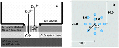 | ||
| Fig. 1 (a) Schematic illustration of a dual-electrode approach for selective Cd detection and (b) schematic of the holes in the perforated carbon, the diameter of the hole is 1 mm. The hole in the center was placed carefully in the center part of the sensing electrode separated by a silicone rubber sheet. | ||
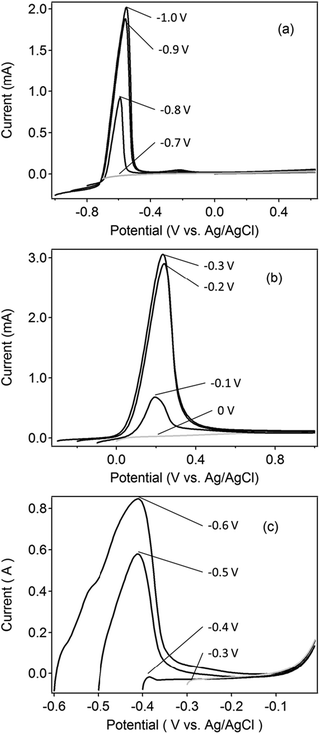 | ||
| Fig. 2 Anodic stripping voltammograms of (a) 0.1 mM Cd2+ solution and (b) 0.1 mM Cu2+ at the perforated carbon electrode, and (c) 0.1 mM Cd2+ at Cu electrodes with various deposition and starting potentials. The electrolyte was 0.1 M HClO4. Deposition was performed for 60 s. The scan rate was 0.3 V s−1. | ||
Results and discussion
The deposition potential of ASV at the BDD electrode was optimized by applying various deposition potentials in two independent solutions of 1 mM Cd2+ and 1 mM Cu2+ in 0.1 M HClO4. The voltammograms, performed from the deposition potential to 0.5 V (data not shown), suggested that the ASV peak of cadmium could be observed using a more negative deposition potential than −0.8 V. Meanwhile, the same experiment with a copper solution suggested that at such a potential value copper was already deposited. These results indicated that, at any possible potential for cadmium deposition, the presence of Cu2+ would interfere with the ASV of Cd2+. The same method at a carbon electrode showed that cadmium and copper started to deposit at −0.8 (Fig. 2a) and −0.2 V (Fig. 2b), respectively. Furthermore, the same experiments using a Cu electrode carried to consider the UPD of Cd on Cu deposited on the carbon electrodes showed that the electrodeposition of cadmium at copper started at the potential of −0.4 V (Fig. 2c). Consequently, the applied potentials for the depleting electrode should be applied between −0.2 V and −0.4 V, whereas for Cd2+ sensing the potential should be more negative than −0.8 V. The deposition potentials of −0.3 V and −1.0 V (vs. Ag/AgCl) were therefore fixed independently at the carbon and BDD electrodes, respectively, for the working electrode system.In order to optimize the copper depletion time as well as the distance between the depleting and the sensing electrodes, a numerical simulation was conducted.
The concentration C of Cu2+ as a function of distance x from the carbon electrode surface and time t of the deposition is governed by Fick's second law:15
 | (1) |
| C(x,0) = C*, 0 < x < l | (2) |
 | (3) |
 | (4) |
 | ||
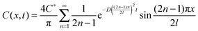
| Fig. 3 (a) Simulated concentration profile of Cu2+ based on eqn (4); (b) Experimental data of ASV for a mixture solution of 0.1 mM Cd2+ and 0.1 mM Cu2+ in 0.1 M HClO4. BDD was used as the sensing electrode with a deposition potential of −1.0 V for 60 s and a scan rate of 0.3 V s−1. A potential of −0.3 V was applied at the carbon electrode for various times to deplete Cu2+. The distance between the BDD and the carbon electrode was fixed at 0.3 mm. A comparison of the dependence on time of C/C* between the simulation data and experimental data extracted from the peak at +0.1 V in (b) is shown in (c). | ||
The simulation demonstrated that, when using a depletion time of 30 s, C/C* at 0.3 mm is reduced by half. In the case of 180 s, almost all of the Cu2+ ions are eliminated. The simulation suggested that a Cu2+-free region could be achieved at the distance of 0.3 mm from the depleting electrodes with an electrolysis time of ∼180 s. Experiments were conducted by positioning the depleting electrode at a distance of 0.3 mm from the sensing electrode for various depletion times. Fig. 3b shows ASV of a mixture solution of 0.1 mM Cd2+ and 0.1 mM Cu2+ in 0.1 M HClO4. While applying a potential of −0.3 V (vs. Ag/AgCl) at the perforated carbon to deplete Cu2+, a potential of +0.5 V was applied at the BDD in order to avoid Cu deposition at the BDD surface. Then, ASV of Cd2+ with a deposition potential of −1.0 V for 60 s was performed at the BDD electrode. It can be seen that without the application of the depleting electrode (depletion time = 0 s) at least four well-defined peaks were observed (Fig. 3b), including a cadmium oxidation peak at −0.6 V, a peak related to copper oxidation at +0.1 V, and two other peaks at −0.05 V and −0.4 V related to the oxidation of Cd–Cu alloys.3,4,14 Increasing the depletion time caused the cadmium-related peak to increase, while on the contrary, the other three peaks decreased. With a depletion time of 180 s, the other three peaks were not clearly observed, indicating that the influence of Cu2+ should be almost negligible.
A comparison of the simulation and experimental data is shown in Fig. 3c. The peak at +0.1 V shown in Fig. 3b was used for the experimental data since it reflects the individual copper species at the surface of the sensing electrode. It can be seen that the simulation data fit quite well with the experimental results. These results suggested that 180 s and longer time for depleting is preferable for the selective Cd detection by using a distance of 0.3 mm.
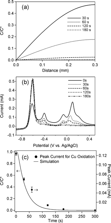
Further simulations and experiments using various positions of the sensing electrodes were also performed. Simulations of implementing different distances between the sensing and the depleting electrodes were shown in Fig. 4a, whereas experimental data for a mixture solution of 0.1 mM Cd2+ and 0.1 mM Cu2+ in 0.1 M HClO4 are displayed in Fig. 4b. A fixed electrolysis time of 120 s was applied for the experiments. At the distance of 1.0 mm, CV shows that all 4 peaks appeared. When the sensing electrodes shifted to the distance of 0.5 mm, the Cd-related peak increased, while other peaks decreased. In the case of 0.3 mm distance, although the peak at ∼0.1 V totally disappeared, the two peaks at ∼−0.4 V and ∼0.0 V remained, suggesting that an electrolysis time of >120 min was required to deplete all copper ions in the 0.3 mm region. The comparison between the simulations and experiments (Fig. 4c) shows that the trend of the experimental results was similar to the simulations.
 | ||
| Fig. 4 (a) Simulated concentration profile of Cu2+ based on eqn (4); (b) Experimental data of ASV for a mixture solution of 0.1 mM Cd2+ and 0.1 mM Cu2+ in 0.1 M HClO4. BDD was used as the sensing electrode with a deposition potential of −1.0 V for 60 s and a scan rate of 0.3 V s−1. A potential of −0.3 V was applied at the carbon electrode at a fixed time of 120 s. Various distances between the BDD and the carbon electrode were examined. A comparison of the dependence on time of C/C* between the simulation data and experimental data extracted from the peak at +0.1 V in (b) is shown in (c). | ||
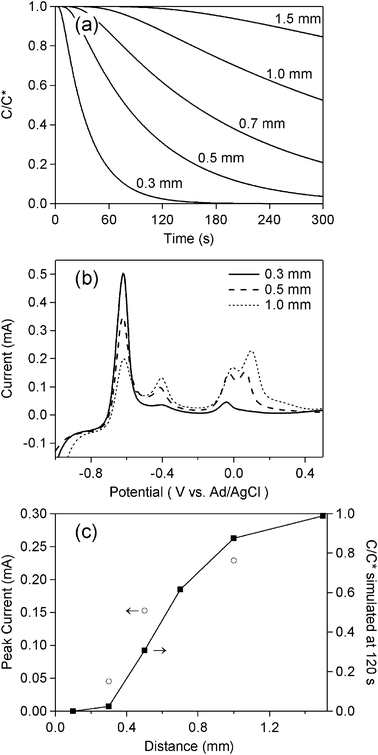
As a model of application, the method was applied for the determination of 0.1 mM Cd2+ in the presence of Cu2+. Fig. 5 shows ASVs for 0.1 mM Cd2+ in the absence of Cu2+ at a single BDD electrode (curve A) in comparison to those for 0.1 mM Cd2+ in the presence of 0.1 mM Cu2+, both without (curve B) and with (curve C) the application of a depletion potential of −0.3 V for 300 s. The figure shows that using this system effectively eliminated the influence of copper, as shown by comparable voltammograms represented by curve A and curve C.
 | ||
| Fig. 5 Linear sweep voltammograms of a solution of 0.1 mM Cd2+ (A), and a solution of 0.1 mM Cd2+ in the presence of 0.1 mM Cu2+ without (B) and with (C) the application of a potential of −0.3 V at the carbon electrode for 180 s. The deposition potential of the BDD electrode was −1.0 V for 60 s with a scan rate of 0.3 V s−1. The distance between the BDD and carbon electrodes was fixed at 0.3 mm. | ||
Considering the total electrolysis of copper, theoretically, with a sample volume of 5.0 mL, a charge of 9.65 × 10⁻² C is required to deposit 0.1 mM Cu2+. In the case of using this method, a volume made by a distance of 0.3 mm from the depleting electrode can be calculated to be ∼0.057 mL. Thus, only a charge of 1.10 × 10⁻⁴ C is required for selective ASV of cadmium. Although, in fact, a charge of 9.8 × 10⁻³ C was observed in the experiment, the higher charge required was reasonable considering that the detecting electrode was positioned in the bottom of the cell. Therefore, the solution was not totally motionless and its transfer to the electrode was influenced by gravitation. On the other hand, converting the theoretical charge of the 5.0 mL volume (9.65 × 10⁻² C) to the applied current of 30 μA (observed from experiment) will need an electrolysis time of ∼3200 s. Moreover, although the electrolysis time can be decreased by increasing the applied current or potential, the procedure was found to affect the deposition of cadmium on deposited copper, suggesting that total electrolysis of copper is not simple and practicable.
The method was also examined for various concentrations of Cd2+. The total charges of Cd oxidation peaks were plotted against Cd2+ concentration. The linear calibration curves are shown in Fig. 6 for 3 repetitive measurements. The small deviation of the curve indicated that good reproducibility of the cadmium peak current could be achieved. Curve A shows the calibration curve of a solution of Cd2+. Curve B shows the linear calibration curve of a solution of Cd2+ in the presence of 0.1 mM Cu2+ without applying the depletion potentials. The figure shows that, although linearity could also be achieved without Cu2+ depletion, the slope is much lower, suggesting low sensitivity for this method. The concentration dependence with the application of the depleting electrode for 180 s (curve C) was similar to curve A, indicating that the method with the dual-electrode is effective for the depletion of Cu2+, at least at 0.3 mm distance. The estimated detection limit was calculated by using yLOD = a + 3 Sy, where Sy is the average deviation obtained for 3 repetitive measurements 0.0029. As the linear calibration curve equation was y = −0.013 + 2.1916x, an estimated detection limit of 443 ppb was obtained. Compared to our previous result,3 the limit of detection was not satisfactory. The probable reason was the limited mass transfer of cadmium above the perforated carbon electrode.
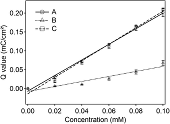 | ||
| Fig. 6 Linear calibration curves of solutions of various concentrations of Cd2+ (A) and solutions of Cd2+, in the presence of 0.1 mM Cu2+, without (B) and with (C) the application of a potential of −0.3 V at the carbon electrode for 180 s. The other conditions are similar to those shown in Fig. 5. | ||
In conclusion, selective anodic stripping voltammetry of trace Cd2+ in the presence of Cu2+ could be achieved by applying two working electrodes, i.e. a copper-depleting electrode (perforated carbon) and a cadmium-sensing electrode (boron-doped diamond). In addition to the deposition potentials, the diffusion profile also became an important factor to be considered. The results indicated that the method is promising for the development of selective detection techniques for any metal ions. Although, the sensitivity still needs to be improved. Furthermore, this method offers a simple and practicable alternative method to solve the problem of selectivity.
Acknowledgements
This work was supported by the New Energy and Industrial Technology Development Organization (NEDO).References
- Diamond Electrochemistry, ed. A. Fujishima and Y. Einaga, et al., BKC, Amsterdam, Boston, Elsevier, Tokyo, 2005 Search PubMed.
- D. Yamada, T. A. Ivandini, M. Komatsu, A. Fujishima and Y. Einaga, J. Electroanal. Chem., 2008, 615, 145 CrossRef CAS.
- S. Fierro, T. Watanabe, K. Akai, M. Yamanuki and Y. Einaga, J. Electrochem. Soc., 2011, 158, F173 Search PubMed.
- O. El Tall, N. Jaffreich-Renault, M. Sigaud and O. Vittori, Electroanalysis, 2007, 19, 1152 CrossRef CAS.
- K. E. Toghill, G. G. Wildgoose, A. Moshar, C. Mulcahy and R. G. Compton, Electroanalysis, 2008, 20, 1731 CrossRef CAS.
- D. Dragoe, N. Spătaru, R. Kawasaki, A. Manivannan, T. Spătaru, D. A. Tryk and A. Fujishima, Electrochim. Acta, 2006, 51, 2437 Search PubMed.
- E. A. McGaw and G. M. Swain, Anal. Chim. Acta, 2006, 575, 180 CrossRef CAS.
- L. A. Hutton, M. E. Newton, P. R. Unwin and J. V. Macpherson, Anal. Chem., 2011, 83, 735 CrossRef CAS.
- S. E. W. Jones, F. G. Chevallier, C. A. Paddon and R. G. Compton, Anal. Chem., 2007, 79, 4110 CrossRef CAS.
- M. I. Aguf, B. G. Karbasov and K. I. Tikhonov, Russ. J. Electrochem., 1996, 32, 718 Search PubMed.
- B. W. Gregory, M. L. Norton and J. L. Stickney, J. Electroanal. Chem. Interfacial Electrochem., 1990, 293, 85 Search PubMed.
- J. Hommrich, S. Humann and K. Wandelt, Faraday Discuss., 2002, 121, 129 RSC.
- S. Humann, J. Hommrich and K. Wandelt, Thin Solid Films, 2003, 428, 76 Search PubMed.
- C. Babyak and R. B. Smart, Electroanalysis, 2007, 19, 1152 CrossRef CAS.
- A. J. Bard and L. R. Faulkner, Electrochemical methods: fundamentals and applications, John Wiley, New York, Chichester, 2nd edn, 2001 Search PubMed.
- K. Wang, D. Zhang, T. Zhou and X. H. Xia, Chem.– Eur. J., 2005, 11, 1341 CrossRef CAS.
- K. Wang, J. J. Xu, D. C. Sun, H. Wei and X. H. Xia, Biosens. Bioelectron., 2005, 20, 1366 CrossRef CAS.
- R. Taniolo, N. Dossi, A. Pizzariello, S. Susmel and G. Bontempelli, Electroanalysis, 2011, 23, 628 CAS.
- T. Watanabe, T. A. Ivandini, Y. Makide, A. Fujishima and Y. Einaga, Anal. Chem., 2006, 78, 7857 CrossRef CAS.
- T. Watanabe and Y. Einaga, Biosens. Bioelectron., 2009, 24, 2684 CrossRef CAS.
- A. C. F. Ribeiro, S. M. N. Simões, V. M. M. Lobo, A. M. T. D. P. V. Cabral, F. J. B. Veiga and M. A. Esteso, J. Chem. Eng. Data, 2009, 55, 2192 Search PubMed.
Footnote |
| † Electronic supplementary information (ESI) available. See DOI: 10.1039/c2cp43283h |
| This journal is © the Owner Societies 2013 |