One-step synthesis of alloyed dual-emitting semiconductor nanocrystals†
Emily J.
McLaurin
,
Majed S.
Fataftah
and
Daniel R.
Gamelin
*
Department of Chemistry, University of Washington, Box 351700, Seattle, Washington 98195-1700, USA. E-mail: gamelin@chem.washington.edu
First published on 6th November 2012
Abstract
Alloyed Zn1−x−yCdxMnySe nanocrystals exhibiting bright intrinsic dual emission attractive for ratiometric optical nanothermometry are reported. Relative to earlier materials with related dual emission, these alloy nanocrystals require shorter syntheses, contain less Cd2+, and show dual emission that is less sensitive to nanocrystal shape, size, or surfaces.
Molecular or nanocrystalline luminophores showing temperature-dependent photoluminescence (PL) can be used for high-resolution thermal mapping of microelectronics, photonics, and biological or biotechnological processes.1,2 Dual-emitting probes provide ratiometric readout that is independent of probe concentration, fluctuations in excitation intensity or detection efficiency, and other local inhomogeneities. Here we describe the development of dual-emitting Mn2+-doped alloy semiconductor nanocrystals as ratiometric probes for optical nanothermometry.
Wide-gap semiconductors doped with Mn2+ have long been used as phosphors in photo- and electroluminescence applications.3,4 Excitation of these semiconductors is followed by rapid energy localization at Mn2+ (kET ∼ 1011 s−1), which emits from its 4T1 state with a high quantum yield (Fig. 1a). Wide-gap Mn2+-doped semiconductor nanocrystals (NCs) behave similarly,5 and are consequently attractive for use in solution-processable electroluminescent devices6,7 and as soluble imaging phosphors.8
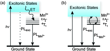 | ||
| Fig. 1 Energy diagrams for Mn2+-doped semiconductors. (a) In wide-gap semiconductors such as ZnSe and ZnS, photoexcitation followed by fast energy transfer to Mn2+ (kET ∼ 1011 s−1) yields efficient sensitized Mn2+ PL (kMn ∼ 104 s−1). (b) Narrowing the semiconductor energy gap brings the excitonic states within thermal reach of the luminescent Mn2+(4T1) excited state, allowing thermal population equilibration and emission from both excited states. | ||
Recently, a new photophysical phenomenon was discovered in this class of materials:9,10 When the excitonic states of Mn2+-doped NCs were tuned to reside just above the lowest Mn2+ excited state (Fig. 1b), thermal equilibration of excited-state populations was found to yield emission from both states. At low temperatures, only Mn2+ PL is observed because population freezes out in the 4T1 state. At high temperatures, only excitonic PL is observed because the excitonic radiative transition probability is ∼104 greater than that of the Mn2+. At intermediate temperatures, dual emission is observed, requiring only ∼1![[thin space (1/6-em)]](https://www.rsc.org/images/entities/char_2009.gif) :104 population of the exciton to achieve equal exciton:Mn2+ PL intensities. This phenomenon, first discovered in quantum-confined Cd1−xMnxSe NCs,9 was most dramatically realized in Zn1−xMnxSe/ZnCdSe core/shell NCs10 and has subsequently been demonstrated in Zn1−xMnxSe/ZnS/CdS/ZnS core/multishell NCs11 and CdSSe/Zn1−xMnxS core/shell NCs.12
:104 population of the exciton to achieve equal exciton:Mn2+ PL intensities. This phenomenon, first discovered in quantum-confined Cd1−xMnxSe NCs,9 was most dramatically realized in Zn1−xMnxSe/ZnCdSe core/shell NCs10 and has subsequently been demonstrated in Zn1−xMnxSe/ZnS/CdS/ZnS core/multishell NCs11 and CdSSe/Zn1−xMnxS core/shell NCs.12
Studies of Zn1−xMnxSe/ZnCdSe NCs showed that the active dual-emission temperature window could be varied by controlling the shell thickness, which in turn controlled the semiconductor energy gap.10 The strong dependence of the NC energy gap on a small number of surface Cd2+ ions, and the extremely strong dependence of the dual emission on this energy gap, resulted in photo- or thermal instabilities of the dual emission in these NCs, however. Such instabilities could be overcome using core/multishell NCs (Zn1−xMnxSe/ZnS/CdS/ZnS) that buffer the energy-tuning CdS layer from both the Mn2+-bearing ZnSe cores and the surfaces.11 Although these multishell NCs are indeed stable at high temperatures and in water, their synthesis requires multiple time-consuming steps that increase size distributions and broaden the dual-emission temperature window.
Here, we report a one-step synthesis of alloyed Zn1−x−yCdxMnySe NCs that, for the first time, yields room-temperature dual-emitting NCs directly out of the synthesis. In contrast with previous studies, the dual emission of these NCs is tuned using composition rather than quantum confinement or shell growth, making it less sensitive to NC shape, size, or surfaces. Moreover, these NCs have the lowest Cd2+ content of any dual-emitting colloidal semiconductor NC to date, a feature of practical interest for many applications.
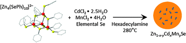
Scheme 1 summarizes the Zn1−x−yCdxMnySe NC synthesis. Modifying a synthesis of Zn1−xMnxSe NCs,13 (Me4N)2[Zn4(SePh)10] tetramers were heated to 280 °C in the presence of CdCl2, MnCl2, and elemental Se using hexadecylamine as a coordinating solvent. Fig. 2a shows absorption spectra of aliquots extracted periodically from a reaction performed with initial values of x = 0.13 and y = 0.06 (see ESI†). The absorption onset redshifts as the reaction temperature is increased and held at 280 °C. The structured spectra at early times are similar to those of small chalcogenide clusters.14 After ∼50 min, the energy gap stops changing but absorption at higher energies continues to increase, suggesting continued deposition of ZnSe onto the NC surfaces. The alloy NCs isolated after 75 min show narrower absorption spectra than our best core/multishell dual-emitting NCs,11 but were prepared in a fraction of the time. Fig. 2b plots cation mole fractions measured by inductively coupled plasma atomic emission spectroscopy (ICP-AES) on precipitated and washed NCs from each aliquot. The Zn2+:Cd2+:Mn2+ ratio remains almost constant over the entire growth period, consistent with nearly homogeneous alloy compositions enriched slightly in ZnSe toward the NC surfaces. The Cd2+ content of these alloy NCs is substantially smaller than in other dual-emitting NCs, with or without Mn2+.10–12,15,16 Incorporation of Cd2+ directly into the Mn2+-doped NC cores reduces the amount needed to achieve the proper energy gap for dual emission by the mechanism of Fig. 1b.
 | ||
| Scheme 1 | ||
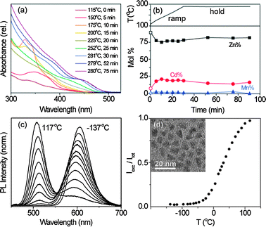 | ||
| Fig. 2 Nanocrystal synthesis and temperature response. (a) Absorption spectra of NC aliquots collected during a reaction, showing a redshift of the absorption onset with reaction time. (b) Top: temperature ramp and hold during synthesis. Bottom: cation mole fractions in precipitated aliquots vs reaction time, measured by ICP-AES. Final composition = Zn0.829Cd0.168Mn0.003Se. (c) Variable-temperature PL spectra of colloidal Zn0.784Cd0.209Mn0.007Se/ZnSe NCs normalized by the total integrated PL intensity. (d) Thermometric response curve (Iexc/Itotvs T) for the NCs of (c), showing a maximum slope of 9.3 × 10⁻³ °C−1. Inset: TEM image of these NCs. Scale bar = 20 nm. | ||
Powder X-ray diffraction (XRD) data for the NCs of Fig. 2b (Fig. S1, ESI†) reveal a zinc blende structure with peaks at angles between those of zinc blende CdSe and ZnSe. Vegard's Law17 suggests x ∼ 0.17, in agreement with ICP results (x = 0.17). The cation composition of the NCs is thus similar to that of the reactants (x = 0.13 in this case), meaning NC energy gaps can be selected simply by adjusting the precursor concentrations in this single-step reaction. This finding is similar to that reported for lyothermal synthesis of Zn1−xCdxSe NCs using ternary decameric clusters [ZnxCd10−xSe4(SePh)12(PnPr3)4],18 but the present results demonstrate that pre-incorporation of Cd2+ or Mn2+ into the clusters prior to thermolysis is not necessary. We also note that similar alloy NCs are obtained using CdO or Cd(OAc)2 instead of CdCl2 (Fig. S2, ESI†), i.e., this synthesis is tolerant of different precursors. By this approach, alloy NCs have been prepared with final Mn2+ concentrations from 0.5% to 2.6%.
Photoluminescence measurements of the alloy NCs from Fig. 2b show pronounced dual emission at room temperature directly out of the synthesis. Similar results have been obtained from several batches, with typical total PL quantum yields of ϕ = 10–30% at room temperature. The quantum yields of these as-prepared NCs are comparable to those of our previous best dual emitting NCs,11 and can be increased even further by ZnSe shell growth via alternating addition of Zn(oleate)2 and TOPSe at 220 °C.19 Fig. S3a (ESI†) shows that ∼2.5 monolayers of ZnSe on Zn0.784Cd0.209Mn0.007Se core NCs increases ϕ from 21.6 ± 0.2% to 45.3 ± 0.1% while shifting the absorption and emission energies only slightly. ZnSe shell growth also narrows the EPR spectrum, reducing the apparent hyperfine coupling constant from a superposition of 89.0 and 61.8 × 10⁻⁴ cm−1 signals to just 61.8 × 10⁻⁴ cm−1, consistent with elimination of surface or adventitious Mn2+ (note: the one-step alloy NC synthesis described above does not involve any surface-cleaning steps).5 Transmission electron microscopy (TEM) images of these alloy/shell NCs (Fig. 2d (inset)) show mostly ∼7.0 nm triangular NCs.
Fig. 2c shows PL spectra of these Zn0.784Cd0.209Mn0.007Se/ZnSe NCs at various temperatures, normalized by their total integrated intensity. Below ∼−100 °C, only Mn2+ PL is observed. This Mn2+ PL is slightly red shifted relative to that in Zn1−xMnxSe NCs (600 vs 590 nm at 22 °C),20,21 tentatively attributed to a low-symmetry splitting of the 4T1 term in the alloy. As the temperature is increased, excitonic PL grows at the expense of Mn2+ PL. At 117 °C, the spectrum shows almost exclusively excitonic PL, shifted from ∼520 to ∼510 nm over this entire temperature range. From the data in Fig. 2c, a thermometric response curve (Iexc/Itotvs T) was constructed (Fig. 2d), which shows a maximum slope of 9.3 × 10⁻³ °C−1 around room temperature, corresponding to a maximum relative sensitivity2 of Sm = (d[Iexc/Itot(Tm)]/dT)/[Iexc/Itot(Tm)] ≈ 2.0% °C−1 that compares favourably with other nanothermometers.2 These metrics do not take into account absorption cross sections, where these semiconductor NCs excel relative to many existing nanothermometers (e.g., lanthanide-doped oxides or fluorides).
The effect of temperature on excited-state populations is illustrated by variable-temperature time-resolved PL decay measurements. Representative data from Zn0.784Cd0.209Mn0.007Se NCs are shown in Fig. 3. At and below −213 °C, only Mn2+ PL is observed, decaying with τMn(avg) ∼ 525 μs (Fig. S4, ESI†). With increasing temperature, τMn decreases slightly due to thermally activated nonradiative processes. At −70 °C (Fig. 3a), τMn(avg) ∼ 450 μs and excitonic PL (∼530 nm) with a comparably slow decay becomes faintly evident. At −18 °C (Fig. 3b), the excitonic PL maximum is shifted to ∼525 nm and has grown more intense. At 19 °C (Fig. 3c), the spectrum is dominated by excitonic PL, which decays with an apparent time constant of ∼70 μs, similar to that of the Mn2+ PL at the same temperature. The excitonic PL displays the signature blueshift with time modelled previously.10 These excitonic PL decay times exceed the intrinsic exciton lifetime by orders of magnitude, reflecting thermal exciton repopulation from the long-lived Mn2+(4T1) excited state. The long exciton decay times and strong temperature dependence seen in Fig. 3 thus illustrate the thermal equilibrium of Fig. 1b.
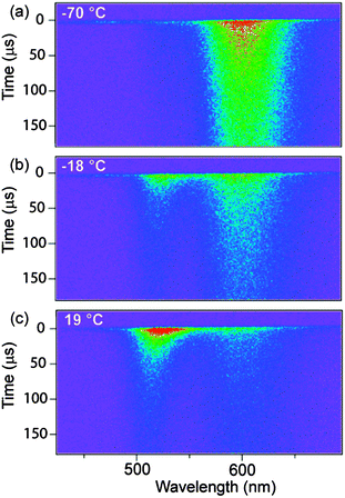 | ||
| Fig. 3 Time-resolved dual emission. PL intensities for Zn0.784Cd0.209Mn0.007Se NCs plotted vs wavelength (horizontal) and time (vertical) for various temperatures. (a) The data at −70 °C show almost exclusively Mn2+ PL with a slow (450 μs) decay. (b) Increasing the temperature to −18 °C causes excitonic PL at ∼525 nm to grow in. (c) At 19 °C, the excitonic PL dominates but retains a long decay time. | ||
An attraction of using alloying rather than quantum confinement9,12 or hetero-shell growth10,11 to tune the NC energy gaps is that this dual emission can now be decoupled from crystal shape and size. To illustrate, Fig. 4 shows normalized variable-temperature PL spectra of dual-emitting Zn0.64Cd0.35Mn0.01Se rods formed by oriented attachment22 of quasi-spherical NCs (Fig. S5, ESI†). As in the NCs, these rods display strongly temperature-dependent dual emission (Fig. 4a), demonstrating this phenomenon for the first time in materials other than quantum dots. Using alloying to tune the exciton–Mn2+(4T1) energy gap, rather than quantum confinement or core/shell growth, thus makes Mn2+-based dual emission accessible in a variety of new crystal morphologies, including anisotropic structures (Fig. 4), heterostructures, and potentially even thin films. As such, the use of alloying introduces new opportunities for the development and application of this class of dual-emitting materials.
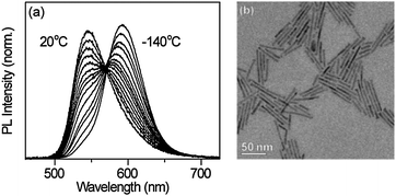 | ||
| Fig. 4 Dual-emitting nanorods. (a) Variable-temperature PL spectra of colloidal Zn0.64Cd0.35Mn0.01Se nanorods, normalized by the total integrated PL intensity. (b) TEM image of the nanorods (∼41 nm long, d ∼ 4 nm). Scale bar = 50 nm. | ||
In summary, a simple, one-step synthesis of Zn1−x−yCdxMnySe alloy NCs has been developed that yields bright, dual-emitting colloidal NCs with high temperature sensitivity. This synthesis is substantially more expedient than previous routes to related dual emitters, and additionally yields NCs in which dual emission is largely decoupled from NC shape and size, making them less susceptible to degradation. These features make dual-emitting alloy NCs particularly attractive for a variety of optical thermometry or thermography applications.
This work was supported by the U. S. National Science Foundation (DMR 1206221). Part of this work was conducted at the University of Washington NanoTech User Facility, a member of the NSF National Nanotechnology Infrastructure Network (NNIN). The authors thank Alina Schimpf, Liam Bradshaw, and Charles Barrows for experimental assistance and Vladimir Vlaskin for valuable discussions.
Notes and references
- D. Jaque and F. Vetrone, Nanoscale, 2012, 4, 4301 RSC.
- C. D. S. Brites, P. P. Lima, N. J. O. Silva, A. Millán, V. S. Amaral, F. Palacio and L. D. Carlos, Nanoscale, 2012, 4, 4799 RSC.
- G. Blasse and B. C. Grabmaier, Luminescent Materials, Springer, Berlin, 1994 Search PubMed.
- Luminescence: From Theory to Applications, ed. C. Ronda, Wiley-VCH, Weinheim, Germany, 2008 Search PubMed.
- R. Beaulac, P. I. Archer, S. T. Ochsenbein and D. R. Gamelin, Adv. Funct. Mater., 2008, 18, 3873 CrossRef CAS.
- H. Yang and P. H. Holloway, J. Phys. Chem. B, 2003, 107, 9705 CrossRef CAS.
- V. Wood, J. E. Halpert, M. J. Panzer, M. G. Bawendi and V. Bulović, Nano Lett., 2009, 9, 2367 CrossRef CAS.
- S. E. Irvine, T. Staudt, E. Rittweger, J. Engelhardt and S. W. Hell, Angew. Chem., Int. Ed., 2008, 47, 2685 CrossRef CAS.
- R. Beaulac, P. I. Archer, J. van Rijssel, A. Meijerink and D. R. Gamelin, Nano Lett., 2008, 8, 2949 CrossRef CAS.
- V. A. Vlaskin, N. Janssen, J. van Rijssel, R. Beaulac and D. R. Gamelin, Nano Lett., 2010, 10, 3670 CrossRef CAS.
- E. J. McLaurin, V. A. Vlaskin and D. R. Gamelin, J. Am. Chem. Soc., 2011, 133, 14978 CrossRef CAS.
- C.-H. Hsia, A. Wuttig and H. Yang, ACS Nano, 2011, 5, 9511 CrossRef CAS.
- V. A. Vlaskin, R. Beaulac and D. R. Gamelin, Nano Lett., 2009, 9, 4376 CrossRef CAS.
- A. Eichhöfer, Eur. J. Inorg. Chem., 2005, 1245 CrossRef.
- A. E. Albers, E. M. Chan, P. M. McBride, C. M. Ajo-Franklin, B. E. Cohen and B. A. Helms, J. Am. Chem. Soc., 2012, 134, 9565 CrossRef CAS.
- A. A. Lutich, C. Mauser, E. Da Como, J. Huang, A. Vaneski, D. V. Talapin, A. L. Rogach and J. Feldmann, Nano Lett., 2010, 10, 4646 CrossRef CAS.
- L. Vegard, Z. Phys. A:Hadrons Nucl., 1921, 5, 17 CAS.
- M. W. DeGroot, H. Rösner and J. F. Corrigan, Chem.–Eur. J., 2006, 12, 1547 CrossRef CAS.
- J. J. Li, Y. A. Wang, W. Guo, J. C. Keay, T. D. Mishima, M. B. Johnson and X. Peng, J. Am. Chem. Soc., 2003, 125, 12567 CrossRef CAS.
- J. F. Suyver, S. F. Wuister, J. J. Kelly and A. Meijerink, Phys. Chem. Chem. Phys., 2000, 2, 5445 RSC.
- D. J. Norris, N. Yao, F. T. Charnock and T. A. Kennedy, Nano Lett., 2001, 1, 3 CrossRef CAS.
- Z. Tang, N. A. Kotov and M. Giersig, Science, 2002, 297, 237 CrossRef CAS.
Footnote |
| † Electronic supplementary information (ESI) available: Additional experimental details and data. See DOI: 10.1039/c2cc36862e |
| This journal is © The Royal Society of Chemistry 2013 |