Super-wetting, wafer-sized silicon nanowire surfaces with hierarchical roughness and low defects†
Ana
Egatz-Gomez
*a,
Ravish
Majithia
ab,
Christopher
Levert
a and
Kenith E.
Meissner
ab
aDepartment of Biomedical Engineering, Texas A&M University, 3120 TAMU, 5032 Emerging Technologies Building, College Station, TX 77843-3120, USA. E-mail: angomez@bme.tamu.edu; Fax: +1 9798454450
bDepartment of Materials Science and Engineering, Texas A&M University, 3120 TAMU, 5032 Emerging Technologies Building, College Station, TX 77843-3120, USA
First published on 18th October 2012
Abstract
This paper reports the fabrication of wafer-sized silicon nanowire (SiNW) surfaces using a modified metal-assisted chemical etching method. The complete fabrication and coating process can be performed in less than three hours, is easily size-scalable, and produces surfaces with very low surface defects, complex, hierarchical surface roughness, and large nanowire height. These surfaces exhibit extreme wettabilities depending on surface coating: oxidized SiNW surfaces are superhydrophilic, while surfaces coated with a fluorinated hydrocarbon are superhydrophobic. The wetting and morphological properties of SiNW surfaces made with one and two etches of different duration are characterized vis-à-vis their effect on water drop mobility. Compared to a single etch process, a double etch followed by coating with a fluorinated hydrocarbon more efficiently produces SiNW surfaces with high contact angles on which microliter-sized water drops roll-off at approximately 0° tilt angle. Due to their very low friction, extreme wetting properties, ease of fabrication, low-cost, and large-sizes, these SiNW surfaces may be advantageous in microfluidic devices, bioanalysis systems sensitive to cross-contamination that require disposable substrates, and other applications.
Introduction
Silicon nanowires (SiNWs) have found application in a growing number of fields because of their compatibility with existing silicon technology, and their structural, electronic, and optical properties. SiNW surfaces have been proposed for photovoltaic solar energy conversion due to their strong optical absorption in the solar spectrum,1 and for thermoelectric energy conversion due to the low thermal conductivity of nanowires.2 SiNWs have also been proposed for field effect transistors (FET).3 SiNW FET-based sensors have been shown to change conductance with electrolyte composition and upon binding/unbinding events to detect protein biomarkers,4,5 small molecules,6,7 DNA,8,9 viruses,10 pH,11 and flow velocity.12 SiNW surfaces coated with epithelial cell antibodies have been used for capture and detection of circulating tumor cells.13 Other uses of SiNWs in bio-applications are further detailed in recent reviews.14–16Of special interest are the wetting properties of SiNW surfaces. Using various surface coatings, the SiNW surfaces can be tuned from superhydrophilic to superhydrophobic.17–20 SiNW superhydrophobic surfaces are particularly attractive as substrates for drop-based microfluidic biochips because the effective contact area between droplets and substrates is very low. This minimizes resistance to drop movement and protein adsorption, and facilitates movement of droplets with high protein concentrations.21 In addition, they hold promise for integration of SiNW-based biosensors on the same substrate used for drop movement. Some examples of applications for droplet manipulation and analysis on open SiNW surfaces include actuation of protein, plasma, and serum drops using magnetic fields and particles,21 electrochemical measurement of dopamine and glucose with magnetic actuation,22 MALDI analysis,23–25 and electrowetting-driven cleaning.26 Two important considerations regarding the use of SiNW surfaces as substrates for biochips are the ability to easily make substrates with a large area, and the production of surfaces with a low number of defects and high nanowire coverage. Large-area substrates allow for mass production of biochips at low-cost, which can be used as disposable substrates to prevent sample contamination. A low number of surface defects and even nanowire coverage across the surface are necessary for uniformity of the macroscopic surface properties and for a reduced number of defective biochips.
There are a variety of methods for fabrication of SiNW surfaces, including vapor-liquid-solid (VLS) chemical vapor deposition, electron-beam lithography, and metal-assisted chemical etching. The VLS mechanism for growth of single crystal SiNWs on silicon substrates (“whiskers”) was introduced almost half a century ago.27 In VLS, liquid alloy droplets are deposited on a silicon substrate. Under a silicon precursor gas, a monocrystalline SiNW forms by precipitation of Si from each alloy droplet. The metallic droplets can be deposited on the wafer surface using a variety of methods, to make either random28,29 or ordered30,31 SiNW surfaces. The size of SiNW surfaces using VLS is limited by the capacity of the chamber where samples are put under high vacuum, high temperature, and explosive, toxic silicon precursor gas. Electron-beam lithography followed by reactive ion etching and thermal oxidation is an alternative fabrication method to produce arrays of regular and hierarchical Si columns.32,33 In addition to the high-cost of an electron lithography system, very long exposure times, typically tens of minutes per square millimeter, are a major limitation of this method.33 SiNW arrays have also been made using metal-assisted chemical etching. This reaction proceeds in an aqueous solution of silver nitrate and hydrofluoric acid (HF). Silver in solution reduces onto the wafer surface forming Ag nanoparticles that oxidize the surrounding Si lattice which is subsequently etched by HF. Further reduction of Ag occurs not on the wafer but on the nanoparticles, which become the active cathode by electron transfer from the underlying wafer. Nanowires and pores are then etched as the Ag nanoparticles sink into the wafer. The principles of metal-assisted chemical etching including the effect of the noble metal, etchant, temperature, and intrinsic properties of the silicon substrate, and fabrication methods including template-based etching are comprehensively detailed in a recent review.34 Metal-assisted chemical etching provides a simple approach to fabricate large, wafer-sized arrays.35 However as we discuss along the following sections, this method presents challenges in obtaining large, defect-free surfaces.
We present a simple, low-cost method for fabrication of wafer-sized SiNW surfaces using a modified version of the metal-assisted chemical etching method that provides enhanced wetting properties due to a combination of large nanowire height, low surface defects, and complex, hierarchical surface roughness with micro to nanometer-sized features. Our experiments show that a double etch followed by coating with a fluorinated hydrocarbon can be used to fabricate wafer-sized SiNW surfaces with contact angles as high as 172°, on which microliter-sized water drops roll off when these surfaces are laid flat, using shorter total etch times compared to SiNW surfaces made using a single etch. As recently pointed out by Cottin-Bizonne et al., small variations in the mesoscopic roughness of a surface can have large effect on its resistance to flow as well as the static wetting properties.36,37 In particular, spiky roughness morphologies offer a very small solid fraction and can produce dramatic friction reductions because they favor a flat, continuous air/water interface between the drop and the surface (“a bubble mattress”).38,39 In our work, the second etch enhances the roll-off effect and reduces friction by reducing or eliminating surface defects remaining from the first etch.
We characterize the wetting and morphological properties of SiNW surfaces made with one and two etches of different duration, and how these properties relate to the roll-off effect. The complete fabrication and coating process can be performed in less than three hours. Due to their very low friction, extreme wetting properties, ease of fabrication, low cost, and large size, which may allow production of multiple disposable chips, these SiNW surfaces are a valuable addition to the existing repertoire of superwetting and antiwetting surfaces,40–42 and may find application in areas such as microfluidic devices and substrates for bioanalysis systems sensitive to cross-contamination.
Experiments and methods
Hydrofluoric acid safety considerations
Some of the procedures presented here use hydrofluoric acid (HF), which is an extremely corrosive acid. Exposure to HF and its fumes, even small amounts, can be fatal. It must be handled only by personnel trained and certified in HF handling, its hazards, and what to do in the event of an exposure or a spill.Materials
Hydrofluoric acid (HF), silver nitrate, nitric acid, acetone, 1H,1H,2H,2H-Perfluorooctyltriethoxysilane (PFOS), and anhydrous toluene were purchased from Sigma- Aldrich (St. Louis, USA). Mechanical grade, 6′′ diameter, n-type silicon wafers, were cleaned by immersion in acetone and ethanol and dried under laboratory compressed air. All HF etching steps were performed in large, round HDPE containers (7′′ diameter, 2 l capacity, Cambro, Huntington Beach, USA) to minimize reagent use and spill risk.SiNW etch
We fabricated SiNW surfaces using a single and double etch. To investigate the effect of the etch time, silicon wafers were etched for 1, 5, 15, 30, and 60 min (t1). The samples etched for 1, 5, 15, and 30 min received an additional etch step of 5 and 15 min (t2). The two etch procedures were identical except for their etch times, as follows. A clean 6′′ diameter silicon wafer was immersed in 160 ml of 0.05 M silver nitrate solution in a HDPE container on a hot plate at 90 °C. Twenty milliliters of 48% HF were added against the wall of the container, around (not over) the wafer under gentle stirring until a silver dendritic film formed over the wafer. The final solution concentration was 5 M HF and 0.04 mM silver nitrate. Upon film formation stirring was stopped to prevent the film from detaching from the wafer surface, and the wafer was etched for t1 min at 90 °C in the HDPE uncovered container. The wafer was then removed with carbon fiber tipped tweezers, and rinsed sequentially as follows: 1) DI water immersion for 3 min to remove the etch solution; 2) nitric acid (40%) immersion for 5 min to remove the silver dendritic film; 3) DI water immersion to remove residual nitric acid; 4) repeat of rinses 3 and 4 with fresh nitric acid solution to completely remove the silver film; and 5) acetone dip to remove loose nanowires. For the second etch, the above steps were repeated using t2 instead t1 min. Hereafter samples made using different etch times are denoted as SiNW_t1 and SiNW_t1+t2, where t indicates the duration of the single etch, and t1+t2 indicate the respective durations of the first (t1) and second (t2) etches (in minutes).Sample coating
Smooth silicon wafers and SiNW surfaces were prepared with three different surface chemistries: a silicon oxide layer, bare silicon, and a fluorinated coating. SiNW surfaces were oxidized by the nitric acid rinses detailed in the previous section. Silicon wafers without native oxide were oxidized by performing the same rinses applied to the nanowire samples (steps 2 to 5). Bare silicon surfaces consisted of SiNW surfaces and smooth silicon wafers, both dipped for 5 to 10 s in 48% HF to remove silicon oxide. For the fluorinated (PFOS) coating, all glassware was thoroughly washed, rinsed with acetone, and dried on a hot plate at 160 °C for 20 min to eliminate as much residual water as possible. Smooth silicon and SiNW surface samples were cleaned by immersion in: 1) 10% hydrofluoric acid for 5 s; 2) DI water for 3 min; and 3) acetone for 5 s; and were dried on a hot plate at 160 °C for 3 min. In a portable glove box under nitrogen atmosphere, samples were immersed in 0.2% v/v PFOS in anhydrous toluene for 30 min. Then samples were rinsed in anhydrous toluene and dried at 120 °C on a hot plate for 20 min.Surface defect image analysis
Ten red-green-blue (RGB) pictures of different regions (54.613 mm2) from a larger SiNW surface (approximately 600 mm2) were taken with a Hirox digital microscope using constant illumination, microscope and camera settings at a magnification yielding 75 pixels/mm2. Image analysis was done with ImageJ v1.46 software.43 Each set of 10 images was treated as a stack. Surface defects were separated from the background using the Color Threshold ImageJ tool, with filters set based on the pixel values of a user-outlined region corresponding to a large defect. Thresholded images were converted to 8-bit black and white images, and defects were measured using the Particle Analysis tool, which provides counts and areas for the surface defects. The defect area was calculated as the total percent total number of white pixels on an image, averaged over the 10 image-stack. The difference between samples was analyzed for statistical significance using t- and F-tests for the percent defect area averages and variances. Sample averages and variances were considered statistically significant when p-values were equal to or lower than 0.05.Contact angle measurements and SEM imaging
Images for contact angle measurements were acquired with a Theta Attension goniometer (Biolin Scientific Inc., Linthicum Heights, MD, USA) and analyzed with ImageJ software.43 Advancing and receding water contact angles were measured by holding a drop on the surfaces using the goniometer's dispensing needle, increasing drop volume to 6 μl, and then reducing the volume. A minimum of 20 measurements of left and right contact angles on 4 drops placed on different surface regions was averaged for each sample type. To test for roll-off effect, a 6 μl drop was dispensed on a surface leveled to 0° and held by the needle, which was then slowly pulled up to allow the drop to detach from the needle (Supplementary Information Fig. 4). Scanning electron microscope (SEM) images of the SiNW surfaces were taken from the top and the side using a JEOL JSM-7500F.Results and discussion
From superhydrophilic to superhydrophobic surfaces
Water contact angles (θ) on surfaces range from 0° to 180°. In general the term superhydrophilic refers to a θ that tends to 0° (complete wetting), hydrophilic to θ < 90°, hydrophobic to θ > 90°, and superhydrophobic to θ > 150°. Additionally, some in the field also require that water drops roll off superhydrophobic surfaces upon tilting the surface by an angle lower than 10°.41,44 The ease with which drops roll off surfaces is enhanced by a higher intrinsic chemical hydrophobicity, a lower wetted surface fraction underneath the drop, texture morphologies with smaller distances between tips and deeper valleys, and hierarchical and complex roughness.41,44,45 Roll-off on superhydrophobic surfaces is closely related to contact angle hysteresis. In general, a small roll-off tilt angle indicates that the surface has very low contact angle hysteresis.46,47 We observed drop roll-off from PFOS-coated SiNW surfaces laid flat (leveled to approximately 0° tilt angle) when drops were gently placed on the surface (minimizing their kinetic energy within our experimental conditions). For this reason, henceforth “roll-off” is used to describe water drops rolling off surfaces that are laid flat, after detaching from the dispensing needle as detailed in the Experiments and methods section.The two main factors that determine the wetting properties of a surface are roughness and chemical composition. We compared two different surface textures, a smooth silicon wafer and a double-etched SiNW surface (SiNW_5+15); and three different surface chemistries, a silicon oxide layer, bare silicon, and silicon with a fluorinated coating. Smooth silicon wafer samples change from hydrophilic to hydrophobic depending on the surface coating. Oxidized smooth silicon wafers are hydrophilic with a contact angle of approximately 38.6°. Bare silicon surfaces are also hydrophilic, with a higher contact angle of 77.0°. Finally, PFOS-coated samples are hydrophobic exhibiting a contact angle of 96.4° (Fig. 1A–C). The change in wetting properties of SiNW surfaces with coating is much more dramatic. SiNW surfaces with an oxide layer are superhydrophilic with a contact angle that tends to zero. Bare SiNW surfaces are hydrophobic with a contact angle of 123.9°. PFOS-coated SiNW surfaces are superhydrophobic with a contact angle of 166.3° (Fig. 1D–F). Videos of Fig. 1 in the ESI illustrate drops falling on SiNW surfaces with the three types of surface chemistry.†
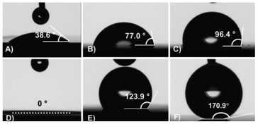 | ||
| Fig. 1 Pictures and contact angle measurements of a 6 μl water drop on: (A) a smooth oxidized silicon wafer; (B) a smooth bare silicon wafer; (C) a smooth PFOS-coated silicon wafer; (D) an oxidized SiNW_5+15 surface (the drop spreads out with a contact angle of approximately 0°, dotted line); (E) a bare SiNW_5+15 surface; and (F) a PFOS-coated SiNW_5+15 surface. The ESI includes videos of drops falling on substrates (D) to (F).† | ||
The relation between the contact angles for the hydrophilic, oxidized smooth (wafer) and rough (SiNW) samples can be described using the Wenzel model. This model describes a regime where the drop fluid wets the surface and fills the gaps in the texture, also called homogeneous wetting. The contact angle of a Wenzel drop is given by:
| cosθ* = rcosθ | (1) |
In Wenzel's model, increasing r makes a hydrophobic surface more hydrophobic and a hydrophilic surface more hydrophilic. In particular, if the roughness of a hydrophilic surface is larger than a critical value given by:
| rc = 1/cosθ | (2) |
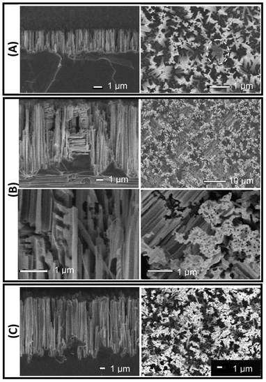 | ||
| Fig. 2 SiNW surfaces SEM images; side-views on left, and top-views on right. (A) A sample made using a single etch of 5 min (SiNW_5) with nanowires are mainly aligned along the vertical direction (side-view). A small area without nanowires is shown on the top-view (inside dotted line). (B) A sample made using a two etches of 5 min (SiNW_5+5). Close-up images are shown on bottom row. The double-etched surface appears as a “mosaic” of regions with horizontal nanowires separated by vertical nanowires (top views). Pores, feather-like structures, and nanowires predominantly in the vertical but also in two mutually perpendicular horizontal directions can be observed on the close-up views. (C) A sample made using an etch of 5 min followed by and etch of 15 min (SiNW_5+15). The top-view shows fewer horizontal nanowires than in (B) due to the longer duration of the second etch. All scale bars correspond to 1 μm, except for the upper right picture in (B), where the scale bar corresponds to 10 μm. | ||
In the Cassie-Baxter or heterogeneous wetting state, drops rest on the tops of the texture leaving air inside the structure, the surface is regarded as an air/solid composite surface, and the Cassie-Baxter contact angle is given by:48
| cosθ* = rsϕcosθ + ϕ − 1 | (3) |
| Surface coating | Experimental | r c | ϕ | Model | |
|---|---|---|---|---|---|
| θ (smooth) | θ* (SiNW) | ||||
| Oxidized silicon | 38.6 | 0.1 | 1.3 | NA | Wenzel |
| Bare silicon | 77.0 | 124.0 | NA | 0.359 | Cassie-Baxter |
| PFOS | 96.4 | 170.1 | NA | 0.016 | Cassie-Baxter |
SiNW surfaces with hierarchical roughness
The effect on surface morphology of the double etch, using different durations for the first (1, 5, 15, and 50 min) and second (5 and 15 min) etches, was elucidated by scanning electron microscopy. Fig. 2 A–C, which consist of side (left) and top (right) views of representative SiNW_5, SiNW_5+5, and SiNW_5+15 surfaces, suggest the following etch mechanism. Assuming the initial surface of the <100>-type wafer is on the x–y plane, during the first etch silver nanoparticles sink into the wafer almost exclusively in the z-direction and produce vertical nanowires (Fig. 2A, side view). After the first etch, un-etched areas or surface defects remain on the surface (discussed in detail in section 3.4), which present alternative crystallographic planes to the nanoparticles during a second etch. Because silver nanoparticles etch silicon preferentially along the three <100> crystallographic directions,52,53 during the second etch silver nanoparticles move predominantly in the z direction, but create complex structures by also etching the newly exposed surfaces in the y and x directions. Examples of these structures are the vertical and horizontal nanowires and “feather-like” structures produced during the second 5-minute etch, shown on Fig. 2B side views (left panel). If the duration of the second etch is increased to 15 min, fewer horizontal SiNWs are observed (Fig. 2C). This may be attributed to the horizontal SiNWs ultimately being etched by nanoparticles moving predominantly in the z direction, and to a distance-dependent interaction between the silver particles that makes the silver particles cooperatively move in the same direction with longer etching times.34,54 Thus, the resulting double-etched surfaces exhibit a more complex morphology with hierarchical roughness as well as decreased defect areas containing no nanostructures.SiNW height was measured on SEM side-views. SiNW average height in samples made with a single etch of 1 to 60 min is 1.03 μm to 15.08 μm; whereas in those made with a total double-etch times (the sum of the first and second etch times) of 6 to 45 min, SiNW height is 5.5 μm to 20.9 μm (Fig. 3A). For single etched surfaces the etch rate decreases from approximately 1.1 μm min−1 after 1 min, to 0.5 μm min−1 and 0.25 μm min−1 after 5 and 60 min, respectively. For double etched surfaces the effective etch rates (using the total etch time) are 0.92 μm min−1 and 0.465 μm min−1 after 6 and 45 min, respectively (Fig. 3B).
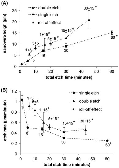 | ||
| Fig. 3 Silicon nanowire height (A) and etch rate (B) for single-etched (circles) and double-etched (triangles) surfaces as a function of the total etch time. In (A) values represent the average height on a SEM image, and error bars represent ±1 standard deviation. Points for double-etched samples correspond to 1 + 5, 5 + 5, 1 + 15, 5 + 15, 15 + 15, and 30 + 15 min. Samples marked with an asterisk exhibit roll-off effect. | ||
Comparing single-etch times to total double-etch times, double-etches produce longer nanowires, provided the duration of the second etch is equal or longer than the duration of the first etch. We also observed that a second etch with a short duration can reduce SiNW length. For example, SiNW_15+5, and SiNW_30+5 samples had an average length shorter than SiNW_15 and SiNW_30, respectively (not shown). The reason for this behavior has not been fully elucidated, but it may be attributed to nanoparticles etching the tips of the SiNWs during the first few minutes until they sink into the pits made by the first etch and lengthen existing SiNWs. Double-etched SiNW surfaces exhibit larger standard deviations of nanowire length that single-etched surfaces (Fig. 3). During the first etch, nanoparticles sink vertically into the wafer at approximately the same rate (Fig. 2A). During the second etch, nanoparticles may either etch surface defects, or sink to the bottom of the pits left by the first etch and lengthen the existing SiNWs, which is the likely cause of the larger variations of nanowire depth of double-etched surfaces (Fig. 2C). This variation for double-etched surfaces can be of several microns.
These results show that a double etch makes it possible to fabricate SiNW surfaces with complex, hierarchical roughness and reduced surface defects, using shorter fabrication times than comparable single-etched surfaces for a given nanowire length. These characteristics can enhance the roll-off effect as discussed in the following sections.
Contact angle and roll-off effect on single- and double-etched PFOS-coated SINW surfaces
In practice, surfaces exhibit a range of static contact angles as a result of roughness morphology, chemical heterogeneity, and drop history (e.g. how it was deposited). The advancing and receding angles are the maximum and minimum values for a liquid front that has been advanced or receded over a surface, and the contact angle hysteresis is the difference between the two.44 We investigated the effect of single and double etches on the PFOS-coated SiNW advancing and receding contact angles and roll-off effect as a function of total etch time (Fig. 4).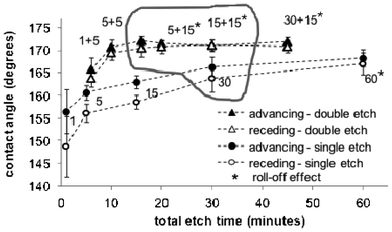 | ||
| Fig. 4 Advancing (black symbols) and receding (white symbols) average water contact angle for SiNW substrates made using a single etch of 1, 5, 15, 30, and 60 min (circles) and a double etch of 1 + 5, 5 + 5, 1 + 15, 5 + 15, 15 + 15, 30 + 15 min (triangles) as a function of the total etch time. Averages correspond to 24 measurements and error bars to ±1 standard deviation. ESI† for Fig. 4: video of a drop on an horizontal SiNW_5+15 surface, first held by the dispensing syringe and then released by slowly pulling the dispensing needle up, illustrating the method used for testing roll-off. | ||
For samples SiNW_1 to SiNW_60, the average advancing contact angle rises from 148.7° to 167°, and the contact angle hysteresis decreases from 7.7° to 1.3°. A 60 min etch was necessary to produce single-etched surfaces with roll-off effect. For double-etched SiNW_1+5 to 1+15 samples, the advancing contact angle increases with total etch time from 165.7° to 172°, and remains approximately constant for longer etch times. The roll-off effect appears for SiNW_1+15 samples and samples made using longer etch times. The angle hysteresis ranges from 1.9° to 0.02°.
The increase of contact angle with etch time for the single-etched samples may be attributed to the combined effects of longer nanowires and reduced surface defects. As nanowires become longer, the drop becomes solely suspended on the tips of the nanowires, and the contact angle is no longer influenced by nanowire length. Our data suggests that the critical length for these samples is around 9 μm (the average nanowire length of the SiNW_1+15 sample), which is also consistent with a previous study on PDMS-coated silicon nanowires.51 By reducing the surface defects, longer etches reduce the solid fraction in contact with the liquid which further increases the contact angle, reduces contact angle hysteresis, and allows roll-off in the case of the SiNW_60 surfaces.
SiNW surfaces shown on Fig. 4 may be grouped in three sets. The first set consists of samples with nanowires equal or shorter than SiNW_5+5 (8.39 μm), which do not exhibit roll off. The surface morphology of SiNW_1+5 and SiNW_5+5 samples, made using short total etch times, appear as a “mosaic” of vertical nanowires separated by horizontal nanowire regions on the order of 10 μm (Fig. 2B, right panel top views). Here, a drop may be more likely to follow the texture rather than to sit on the tips of the vertical nanowires, resulting in the lower observed contact angles and no roll-off effect. The samples in the second set (grouped with a thick grey line) all have similar nanowire lengths and contact angles (9.10 μm to 12.82 μm and 166.02° to 171.1°). In this group, the double-etched samples exhibit a smaller contact angle hysteresis than the single-etched samples and the roll-off effect. In the third set, there is a single- and a double-etched surface. Both are roll-off surfaces with the larger nanowires (15.18 and 20.82 μm), contact angles (170.35° and 172.18°), and etch times (60 and 45 min), and small contact angle hysteresis (1.2° and 1.07°).
These results show that a double etch makes it possible to fabricate roll-off superhydrophobic surfaces using reduced fabrication times than comparable single-etched surfaces. The roll-off effect appeared sooner for double-etched surfaces (marked with asterisks on Fig. 3 and 4). Drops rolled-off double-etched surfaces made with a total etch time of 16 min (SiNW_1+15), while a 60 min etch was necessary for the roll-off effect to appear on single-etched surfaces. The second etch enhances aspects of surface morphology that contribute to a reduction of surface friction and development of roll-off, such as the introduction of complex roughness which favours entrapment of air bubbles beneath the drops, and reduction of surface defects which reduces the contact angle hysteresis, discussed in the following section.
Reduction of defects on SiNW surfaces
Metal-assisted etching of SiNWs is a simple method for fabrication of large silicon nanowire surfaces. However, achieving a defect-free surface with this method can be challenging. Surface defects contribute to surface roughness heterogeneity and can hinder the macroscopic wetting properties of SiNW surfaces. As in other wet-etch methods, generation of gas bubbles produces spot-shaped surface defects. In addition, large concentration gradients that arise during the immersion of the silicon wafer in a pre-mixed HF–silver nitrate solution produce wave-shaped surface defects due to non-homogeneous silver reduction on the wafer's surface. We found that these problems can be mitigated by using a double etch, and placing the wafer in a silver nitrate solution and then slowly adding HF to the solution, allowing it to diffuse over the wafer rather than dipping the wafer into the pre-mixed solution. Surface defects appear as shiny spots, some of them detectable to the naked eye. SEM imaging revealed that these spots correspond to areas without or with very short SiNWs. Fig. 5A shows images of SiNW surfaces made with a single etch of 1, 5, 15, 30, and 60 min. The surface color changes from black to greenish-brown as etch times increase. This increase in reflectivity has recently been attributed to bundle formation as SiNWs become longer yielding an increase in void space between nanowires.55 Consistent with this we observe that reflectivity in general increases with longer etch times for the single-etched and for the double-etched SiNW surfaces, as image histograms shift toward higher intensities for the more reflective surfaces. Fig. 5B shows representative 6.40 mm × 8.53 mm close-up pictures of bare SiNW_1, SiNW_30, and SiNW_5+15 surfaces, on which surface defects appear as light-colored spots. Defects decrease in number for the SiNW_30 sample, and are barely noticeable on the SiNW_5+30 sample. Defects were separated from the background using an ImageJ built-in color thresholding method based on the pixel color values of a user-defined defect region. The segmentation method was chosen due to the changing surface reflectivity, the absence of well-defined peaks and valleys on the image histograms, the small defect size, and the distinct defect color compared to the background.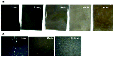 | ||
| Fig. 5 Macroscopic and mesoscopic SiNW surface images. (A) Pictures of SiNW surfaces (approximately 30 mm × 20 mm), made with a 1, 5, 15, 30, and 60 min single etch, taken with a digital camera, illustrating SiNW surface color changes from black to greenish-brown as nanowires are longer. (B) Pictures of SiNW surfaces (6.40 mm × 8.53 mm), made with a single etch of 1 and 30 min and a double etch of 5 + 15 min, taken with a digital inspection microscope. The white spots on the images correspond to surface defects, i.e., highly reflective areas without nanowires or with very short nanowires. | ||
As shown in Fig. 6A, long single etches can reduce the size and number of surface defects. For example, a single etch of 60 min produces a low-defect surface and facilitates the roll-off effect. Still, a disadvantage of this approach is that longer SiNWs tend to break apart from the surface.2 Double etching eliminates most large and medium-sized defects (greater than 0.002 mm2). For double-etched surfaces, the averages and variances of percent defect area are from one to two orders of magnitude smaller than for single-etched surfaces, and the minimum percent defect area is close to zero (Fig. 6B and Table 1). Table 2 shows the results of one-tailed statistical significance t- and F-tests for comparisons between the average and variance of the percent defect area of the SiNW samples taken by pairs. Differences between sample averages and variances are considered statistically significant when the test p-value is 0.05 or lower. The significance levels for the average percent defect area are shown on the upper triangular matrix of Table 2 with number signs, and for the variance on the lower triangular matrix with asterisks. From the p-values, it can be concluded that a single etch of at least 30 min is necessary to achieve a significant reduction in percent defect area and its variance, and that double etching significantly reduces the percent defect area and its variance relative to single etches. The exception is SiNW_1+5, which is the double-etched sample made with the shortest total etch time (6 min), compared to SiNW_60, whose etch time is ten times longer (60 min). The percent average area for SiNW 1+5 is significantly lower than for SiNW_60 but the variances are not significantly different.
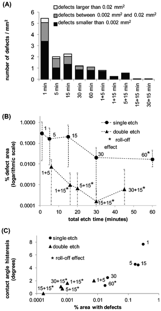 | ||
| Fig. 6 Analysis of surface defects. (A) Number of defects per unit area, classified in three groups according to defect size: x < 0.0002 mm2 (1 pixel), 0.0002 mm2 < x < 0.02 mm2 (from 2 to 100 pixels), and 0.002 mm2 < x (defects larger than 100 pixels). (B) Percentage area with defects, calculated as the average percent defect area measured on 10 different regions (54.5 mm2) of a larger SiNW surface sample (approximately 600 mm2). The surfaces were made by single (circles) and double (triangles) etches using selected times. Error bars indicate maximum and minimum defect area measurements. (C) Contact angle hysteresis (difference between the advancing and receding contact angles shown on Fig. 4), plotted as a function of percentage defect area for single and double etched SiNW surfaces. | ||
| Etch time (min) | Mean | Variance | 1 | 15 | 30 | 60 | 1 + 5 | 1 + 15 | 5 + 15 | 15 + 15 | 30 + 15 |
|---|---|---|---|---|---|---|---|---|---|---|---|
| 1 | 3.0 × 10⁻¹ | 1.0 × 10⁻¹ | — | # | ## | ## | ## | ## | ## | ## | |
| 15 | 2.1 × 10⁻¹ | 5.2 × 10⁻² | — | # | # | # | # | # | # | # | |
| 30 | 2.1 × 10⁻² | 4.5 × 10⁻⁴ | ** | ** | — | # | ## | ## | ## | ## | |
| 60 | 1.7 × 10⁻² | 1.3 × 10⁻⁴ | ** | ** | * | # | ## | ## | ## | ## | |
| 1 + 5 | 7.4 × 10⁻³ | 7.5 × 10⁻⁵ | ** | ** | ** | — | # | # | # | # | |
| 1 + 15 | 9.7 × 10⁻⁴ | 1.5 × 10⁻⁶ | ** | ** | ** | ** | ** | — | # | — | |
| 5 + 15 | 6.8 × 10⁻⁴ | 1.3 × 10⁻⁶ | ** | ** | ** | ** | ** | — | — | — | |
| 15 + 15 | 1.6 × 10⁻⁴ | 7.7 × 10⁻⁸ | ** | ** | ** | ** | ** | ** | ** | — | |
| 30 + 15 | 6.1 × 10⁻⁴ | 3.0 × 10⁻⁶ | ** | ** | ** | ** | ** | — | — | ** |
On Fig. 6C, we plot the contact angle hysteresis from data on Fig. 4 as a function of the percent defect area for the single- and double-etched surfaces. These results clearly show that reduced surface defects lead to a very small contact angle hysteresis and roll-off effect on SiNW surfaces.
Conclusions
We have described and investigated a modified version of the metal-assisted etch method that uses two shorter etches to replace a conventional single long etch. This technique enables large-scale production of wafer-sized SiNW surfaces with tunable wettability. The complete fabrication and coating process can be performed in less than three hours. SiNW surfaces with a silicon oxide layer exhibit superhydrophilic behavior, while SiNW coated with a fluorinated hydrocarbon (PFOS) are superhydrophobic, with a tendency of droplets to roll off easily from surfaces leveled to approximately 0° tilt angle. The second etch enhances the roll-off and superhydrophobic properties of these surfaces by reducing surface defects, generating surfaces with a complex, random, hierarchical surface roughness, and producing large nanowire heights using total etch times as short as 16 min. Due to their very low friction, extreme wetting properties, ease of fabrication, low cost, and large size, these SiNW surfaces may be easily adapted to microfluidic device applications that are sensitive to cross-contamination and require disposable substrates.Acknowledgements
AEG thanks funding from the Department Bioengineering Department, Texas A&M University. RM and KEM acknowledge partial funding from NSF through CBET grant 0933719.References
- K. Q. Peng and S. T. Lee, Adv. Mater., 2011, 23, 198–215 CrossRef CAS.
- A. I. Hochbaum, R. Chen, R. D. Delgado, W. Liang, E. C. Garnett, M. Najarian, A. Majumdar and P. Yang, Nature, 2008, 451, 163–167 CrossRef CAS.
- Y. Cui, Z. Zhong, D. Wang, W. U. Wang and C. M. Lieber, Nano Lett., 2003, 3, 149–152 CrossRef CAS.
- G. Zheng, F. Patolsky, Y. Cui, W. U. Wang and C. M. Lieber, Nat. Biotechnol., 2005, 23, 1294–1302 CrossRef CAS.
- S. M. Kwon, G. B. Kang, Y. T. Kim, Y. H. Kim and B. K. Ju, J. Nanosci. Nanotechnol., 2011, 11, 1511–1514 CrossRef CAS.
- W. U. Wang, C. Chen, K. H. Lin, Y. Fang and C. M. Lieber, Proc. Natl. Acad. Sci. U. S. A., 2005, 102, 3208–3212 CrossRef CAS.
- M. C. McAlpine, H. D. Agnew, R. D. Rohde, M. Blanco, H. Ahmad, A. D. Stuparu, W. A. Goddard Iii and J. R. Heath, J. Am. Chem. Soc., 2008, 130, 9583–9589 CrossRef CAS.
- Z. Gao, A. Agarwal, A. D. Trigg, N. Singh, C. Fang, C. H. Tung, Y. Fan, K. D. Buddharaju and J. Kong, Anal. Chem., 2007, 79, 3291–3297 CrossRef CAS.
- L. T. H. Kao, L. Shankar, T. G. Kang, G. Zhang, G. K. I. Tay, S. R. M. Rafei and C. W. H. Lee, Biosens. Bioelectron., 2011, 26, 2006–2011 CrossRef CAS.
- F. Patolsky, G. Zheng, O. Hayden, M. Lakadamyali, X. Zhuang and C. M. Lieber, Proc. Natl. Acad. Sci. U. S. A., 2004, 101, 14017–14022 CrossRef CAS.
- X. T. Vu, R. Stockmann, B. Wolfrum, A. Offenhäuser and S. Ingebrandt, Phys. Status Solidi A, 2010, 207, 850–857 CrossRef CAS.
- D. R. Kim, C. H. Lee and X. Zheng, Nano Lett., 2009, 9, 1984–1988 CrossRef CAS.
- S. Wang, G. E. Owens and H. R. Tseng, Methods Mol. Biol., 2011, 726, 141–150 CAS.
- A. K. Wanekaya, W. Chen, N. V. Myung and A. Mulchandani, Electroanalysis, 2006, 18, 533–550 CrossRef CAS.
- B. K. Teo and X. H. Sun, Chem. Rev., 2007, 107, 1454–1532 CrossRef CAS.
- Y. He, C. Fan and S.-T. Lee, Nano Today, 2010, 5, 282–295 CrossRef CAS.
- R. Rosario, D. Gust, A. A. Garcia, M. Hayes, J. L. Taraci, T. Clement, J. W. Dailey and S. T. Picraux, J. Phys. Chem. B, 2004, 108, 12640–12642 CrossRef CAS.
- A. Egatz-Gómez, S. Melle, A. A. García, S. A. Lindsay, M. Márquez, P. Domínguez-García, M. A. Rubio, S. T. Picraux, J. L. Taraci, T. Clement, M. Hayes and D. Gust, Appl. Phys. Lett., 2006, 89, 034106 CrossRef.
- G. Piret, Y. Coffinier, C. Roux, O. Melnyk and R. Boukherroub, Langmuir, 2008, 24, 1670–1672 CrossRef CAS.
- G. Piret, E. Galopin, Y. Coffinier, R. Boukherroub, D. Legrand and C. Slomianny, Soft Matter, 2011, 7, 8642–8649 RSC.
- A. A. Garcia, A. Egatz-Gómez, S. A. Lindsay, P. Dominguez-Garcia, S. Melle, M. Marquez, M. A. Rubio, S. T. Picraux, D. Yang and P. Aella, J. Magn. Magn. Mater., 2007, 311, 238–243 CrossRef CAS.
- S. Lindsay, T. Vázquez, A. Egatz-Gómez, S. Loyprasert, A. A. Garcia and J. Wang, Analyst, 2007, 132, 412–416 RSC.
- M. L. McLauchlin, D. Yang, P. Aella, A. A. Garcia, S. T. Picraux and M. A. Hayes, Langmuir, 2007, 23, 4871–4877 CrossRef CAS.
- G. Piret, H. Drobecq, Y. Coffinier, O. Melnyk and R. Boukherroub, Langmuir, 2009, 26, 1354–1361 CrossRef.
- F. Lapierre, G. Piret, H. Drobecq, O. Melnyk, Y. Coffinier, V. Thomy and R. Boukherroub, Lab Chip, 2011, 11, 1620–1628 RSC.
- M. Jonsson-Niedziolka, F. Lapierre, Y. Coffinier, S. J. Parry, F. Zoueshtiagh, T. Foat, V. Thomy and R. Boukherroub, Lab Chip, 2011, 11, 490–496 RSC.
- R. S. Wagner and W. C. Ellis, Appl. Phys. Lett., 1964, 4, 89–90 CrossRef CAS.
- J. Westwater, D. P. Gosain, S. Tomiya, S. Usui and H. Ruda, J. Vac. Sci. Technol., B, 1997, 15, 554–557 CAS.
- A. Egatz-Gómez, J. Schneider, P. Aella, D. Yang, P. Domínguez-García, S. Lindsay, S. T. Picraux, M. A. Rubio, S. Melle and M. Marquez, Appl. Surf. Sci., 2007, 254, 330–334 CrossRef.
- X. Y. Zhang, L. D. Zhang, G. W. Meng, G. H. Li, N. Y. Jin-Phillipp and F. Phillipp, Adv. Mater., 2001, 13, 1238–1241 CrossRef CAS.
- B. Fuhrmann, H. S. Leipner, H.-R. Höche, L. Schubert, P. Werner and U. Gösele, Nano Lett., 2005, 5, 2524–2527 CrossRef CAS.
- H. Liu, J. Vac. Sci. Technol., B, 1992, 10, 2846 CAS.
- J. Feng, M. T. Tuominen and J. P. Rothstein, Adv. Funct. Mater., 2011, 21, 3715–3722 CrossRef CAS.
- Z. Huang, N. Geyer, P. Werner, J. de Boor and U. Gösele, Adv. Mater., 2011, 23, 285–308 CrossRef CAS.
- K. Q. Peng, Y. J. Yan, S. P. Gao and J. Zhu, Adv. Mater., 2002, 14, 1164 CrossRef CAS.
- C. Cottin-Bizonne, J.-L. Barrat, L. Bocquet and E. Charlaix, Nat. Mater., 2003, 2, 238–240 CrossRef.
- C. Cottin-Bizonne, C. Barentin, Ã. Charlaix, L. Bocquet and J. L. Barrat, Eur. Phys. J. E, 2004, 15, 427–438 CrossRef CAS.
- A. Steinberger, C. Cottin-Bizonne, P. Kleimann and E. Charlaix, Nat. Mater., 2007, 6, 665–668 CrossRef CAS.
- A. Steinberger, C. Cottin-Bizonne, P. Kleimann and E. Charlaix, Phys. Rev. Lett., 2008, 100, 134501 CrossRef CAS.
- X. J. Feng and L. Jiang, Adv. Mater., 2006, 18, 3063–3078 CrossRef CAS.
- P. Roach, N. J. Shirtcliffe and M. I. Newton, Soft Matter, 2008, 4, 224–240 RSC.
- Y.-L. Zhang, H. Xia, E. Kim and H.-B. Sun, Soft Matter, 2012 10.1039/c2sm26517f.
- T. J. Collins, BioTechniques, 2007, 43, 25–30 CrossRef.
- C. Dorrer and J. Ruhe, Soft Matter, 2009, 5, 51–61 RSC.
- C. W. Extrand, Langmuir, 2006, 22, 1711–1714 CrossRef CAS.
- A. Marmur, Langmuir, 2004, 20, 3517–3519 CrossRef CAS.
- B. Bhushan and Y. C. Jung, Prog. Mater. Sci., 2011, 56, 1–108 CrossRef CAS.
- M. Callies and D. Quere, Soft Matter, 2005, 1, 55–61 RSC.
- N. J. Shirtcliffe, G. McHale, M. I. Newton, G. Chabrol and C. C. Perry, Adv. Mater., 2004, 16, 1929–1932 CrossRef CAS.
- Y.-H. Cheng, C.-K. Chou, C. Chen and S.-Y. Cheng, Chem. Phys. Lett., 2004, 397, 17–20 CrossRef CAS.
- C. Y. Kuo and C. Gau, J. Electrochem. Soc., 2010, 157, K201–K205 CrossRef CAS.
- K. Peng, A. Lu, R. Zhang and S. T. Lee, Adv. Funct. Mater., 2008, 18, 3026–3035 CrossRef CAS.
- H. Chen, H. Wang, X. H. Zhang, C. S. Lee and S. T. Lee, Nano Lett., 2010, 10, 864–868 CrossRef CAS.
- Z. Huang, T. Shimizu, S. Senz, Z. Zhang, X. Zhang, W. Lee, N. Geyer and U. Gösele, Nano Lett., 2009, 9, 2519–2525 CrossRef CAS.
- B. Ozdemir, M. Kulakci, R. Turan and H. E. Unalan, Nanotechnology, 2011, 22, 155606 CrossRef.
Footnote |
| † Electronic Supplementary Information (ESI) available. See DOI: 10.1039/c2ra22267a |
| This journal is © The Royal Society of Chemistry 2012 |