Recycle and reuse of substrates and the deposit materials†
Amitha
Shetty
and
Karuna Kar
Nanda
*
Materials Research Centre, Indian Institute of Science, Bangalore, India. E-mail: nanda@mrc.iisc.ernet.in.; Fax: +91-80-2360 7316; Tel: +91-80-2293 2996
First published on 2nd October 2012
Abstract
The recovery and reuse of substrates such as indium tin oxide (ITO) and silicon along with the deposited materials has been attempted for the first time. It has been possible to exfoliate the oxide nanostructured films by a conducting polymer named poly-(3,4-ethylenedioxythiophene):poly-(styrenesulphonic acid)(PEDOT:PSS), leaving the substrates unaltered, so they can be used several times without any degradation of the material properties. One of the by-products is the retrieval of a flexible and free-standing inorganic–organic hybrid structure, which on annealing in an Ar atmosphere recovers the oxide materials from the hybrid structure.
Indium tin oxides (ITOs) are used in countless diverse applications as they offer the best performances in terms of optical transparency, electrical resistivity, uniformity of both transparency and resistivity, chemical and mechanical stability, resistance to corrosion, etc. They are the best materials for opto-electronic devices such as light emitting diodes, solar cells and flat panel displays.
The use of ITO is increasing day by day as ITOs are also widely used by researchers for the deposition of thin films and nanostructures for different studies such as substrates for optical characterization and electrodes for light emitting and solar cell applications, etc. Because of an increasing focus on green energy technology, the usage of ITO is expected to increase even more. The main concern about ITO is the cost and the rise of its price. The price for 1.0 cm2 of ITO is in the $3–$25 range depending on its resistivity and thickness.1 The projected scarcity of metals may cause the price to rise further.2 Significant efforts have been made to develop alternative transparent conducting materials. Aluminum zinc oxide (AZO) is a common choice of transparent conducting oxide (TCO) because of its cost and relatively good optical transmission performance in the solar spectrum. Apart from AZO, other materials that can probably replace ITO are fluorine doped tin oxide, carbon nanotubes, graphene, graphene oxide, metal thin films and conductive polymers.3–12 The quest is on to find a suitable replacement for ITO. However, the materials developed thus far are not able to match the performance of ITO.
One of the solutions for the increasing demand of ITO is recycling, which has not been envisioned yet for nanoparticle research. Here, a simple method of lifting oxide nanorods from the ITO substrate is described. Characterization of fresh and used ITOs suggests that they can be recycled. One of the interesting byproducts of the exfoliation process is the fabrication of a free standing oxide nanorod–PEDOT:PSS heterojunction. PEDOT:PSS is known to be one of the p-type materials that forms a heterojunction with n-type oxides.13,14 It has also been shown that the oxide materials from hybrid structures can be recovered by annealing the heterojunction in an Ar atmosphere. Overall, the present work describes the recovery and reuse of the substrates and the deposited materials.
The sample microstructure is characterized by scanning electron microscopy (SEM) using a field emission scanning microscope (FESEM, Serion). Electron dispersive X-ray spectroscopy (EDS) analysis in the SEM is used to determine the film compositions. An Asylum Research MFP-3DSA atomic force microscope (AFM) is used to examine the surface morphologies of the samples. The optical properties are measured using a UV-Vis Hitachi U-3000 spectrophotometer. X-ray photoelectron spectroscopy (XPS) studies are carried out using an ESCA-3 Mark II spectrometer (VG Scientific Ltd., England) using Al-Kα radiation. Raman and photoluminescence spectra are recorded on a LABRAM-HR spectrometer (Jobin-Yvon) excited with 514 and 325 nm lasers, respectively.
A schematic diagram of the exfoliation of the nanostructured film is shown in Scheme 1. Exfoliation is not only possible for nanorods but also for microstructures, as depicted in Scheme 1. A drop of PEDOT:PSS is cast onto the deposit and allowed to dry under a tungsten lamp. The temperature of the films as measured using a laboratory thermometer is 60 °C when the lamp is on. After about 40 min, the PEDOT:PSS with oxide nanorods partially embedded in it is exfoliated. The exfoliation starts from the periphery and proceeds to the middle. First, the exfoliation of ZnO nanorods is discussed. It has been reported that a strong interaction between the thiophene molecules of PEDOT:PSS and ZnO nanoparticles exists. As a result, a red shift in the Raman spectrum of the ZnO–PEDOT:PSS composite is observed.18 In order to investigate the interaction between ZnO and PEDOT:PSS, a composite is prepared by thoroughly mixing 6.25 mg of ZnO in 1500 μL of PEDOT:PSS and then drying under a lamp. Raman spectra of both PEDOT:PSS and the PEDOT:PSS–ZnO composite are compared in Fig. 1a. A red shift in the spectrum of the composite is observed, which confirms the interaction between ZnO and PEDOT:PSS.15 There was no shift observed in the case of an exfoliated film as the interaction between the polymer and ZnO is only limited to the surface. In order to illustrate the thermo-mechanical properties of the PEDOT:PSS film, it is kept under a ruler under an incandescent light. It is observed that there is a contraction in the length of the film in the presence of the light as shown in Fig. 1b,c. Overall, the strong interaction between ZnO and PEDOT:PSS and the thermo mechanical response of PEDOT:PSS enables one to exfoliate the ZnO from ITO. In this context, it is worthy to note that spin coated PEDOT:PSS does not exfoliate the ZnO film. The interaction between PEDOT:PSS and the materials should be stronger than that between the materials and the substrates for the exfoliation to occur.
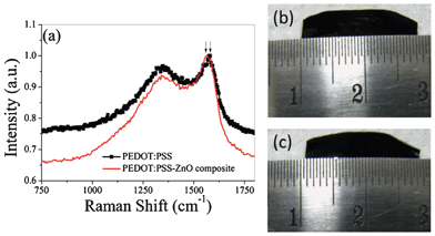 | ||
| Fig. 1 PEDOT:PSS–ZnO interaction. (a) Raman spectra of PEDOT:PSS and the ZnO–PEDOT:PSS composite. (b) and (c) Optical photographs of PEDOT:PSS before and after exposure to a tungsten lamp. | ||
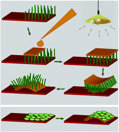 | ||
| Scheme 1 Schematic showing the steps involved in the exfoliation of nanostructures of different morphologies. | ||
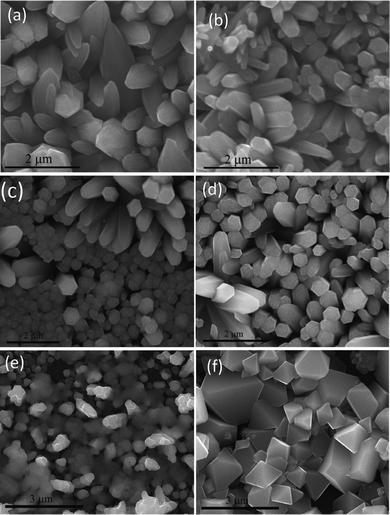
The SEM micrograph of an electrochemically deposited ZnO film with the exfoliated region is shown in Fig. 2a. We have also successfully exfoliated ZnO nanostructures and Ga2O3 nanostructures from both ITO and silicon synthesized by microwave-assisted techniques16 and the SEM micrographs are shown Fig. 2b and c. The SEM micrograph of Ga2O3 microstructures in the non-exfoliated region is shown in the inset of Fig. 2c. This indicates that not only nanorods but also microstructures can be exfoliated.
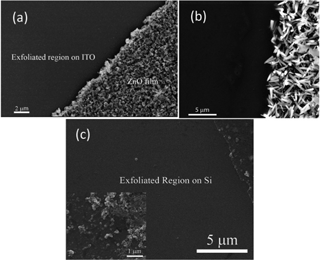 | ||
| Fig. 2 SEM micrographs of the exfoliated region. ZnO nanostructures are prepared by (a) electrochemical deposition on ITO and (b) microwave-assisted growth on silicon. (c) Ga2O3 microstructures are prepared by microwave-assisted growth on silicon. | ||
The optical as well as electrical properties were studied to ascertain the quality of the used ITO/silicon. A comparison of the current–voltage characteristics of fresh ITO and used ITO are shown in Fig. 3a and the transmittance spectra are shown in Fig. 3b. The identical characteristics of fresh ITO and used ITO reveal that they can be recycled. XPS studies reveal a small amount of Zn [Fig. 3c] that is not traceable from energy dispersive X-ray spectroscopy (EDS). A small amount of ZnO is seen from the SEM micrograph [Fig. 3d]. The contribution of Zn comes from the broken ZnO nanorods on the ITO. However, no Zn is traceable from XPS studies in the case of silicon substrates [Fig. 3c]. The broken ZnO nanorods were then removed by rinsing the used substrates with acetone. AFM micrographs as shown in Fig. 3e,f reveal that the morphology of the fresh and used ITO is identical. As a conducting substrate is essential for an electrochemical deposition of materials, we investigated the recycling of ITO for the deposition of ZnO. It requires ZnO to be deposited on ITO as a ZnO–ITO heterojunction can be used as a basis for different applications such as solar cells, light emitting devices and photodetectors.17–19 We are able to grow identical morphologies of ZnO after several uses as shown in Fig. 4(a–d). It may be noted that one-dimensional nanostructures such as nanorods of ZnO are obtained by electrochemical deposition and ITO can be used several times. Not only electrochemically deposited ZnO but also that deposited by other techniques such as microwave-assisted techniques16 can successfully be exfoliated. Other oxides such as NiO and Cu2O oxide are grown on the ITO substrates [Fig. 4(e and f)] and are successfully exfoliated.
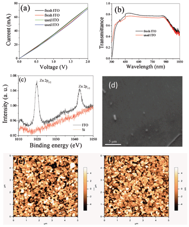 | ||
| Fig. 3 Characterization of used substrates. (a) I–V curves of fresh and used ITO. (b) Optical transmittance of the fresh and used ITO showing similar behaviour with no degradation of the coating. (c) XPS measurements on the used ITO and used Si showing the signal of ZnO traces. (d) SEM micrograph showing the traces of ZnO on used ITO. (e,f) AFM micrographs taken on fresh and used ITO showing similar morphology. | ||
 | ||
| Fig. 4 Recycling tests. SEM micrographs of the ZnO nanorods grown on the same substrate. (a) 1st, (b) 2nd, (c) 3rd, (d) 4th depositions; (e) nickel oxide and (f) copper oxide film. | ||
The cost factor of ITO and silicon is one of the barriers for wide use. When the cost is taken into consideration the cost associated with the recycling of substrates is much cheaper. Improvements in the speed and efficiency of ITO will provide sufficient indium for all other applications and will eventually bring about price stability. Not only ZnO from ITO, but also ZnO from Si and sapphire, and Ga2O3 from Si can be exfoliated and a heterojunction of ZnO–PEDOT:PSS and Ga2O3–PEDOT:PSS films can be fabricated. This suggests that the recycling of ITO and other substrates such as silicon/sapphire is possible for other nanoresearch.
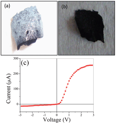
Another interesting byproduct of the process is the retrieval of a flexible hybrid structure of ZnO nanorods and PEDOT:PSS. It may be noted that the fabrication of the free-standing heterojunction is a major challenge. One side is PEDOT:PSS and the other side is ZnO. The ZnO side of the film appears white while the PEDOT:PSS side is black in color. Optical micrographs of the PEDOT:PSS and ZnO sides of the free film are shown in Fig. 5a,b. EDS spectra of both sides of an exfoliated film are shown in Fig. S1.† As expected, the ZnO side shows the presence of Zn and O whereas the polymer side shows the presence of sulphur (S) along with C, O and Na, as expected. The current–voltage characteristics of a free-standing heterojunction with a Ag/ZnO/PEDOT:PSS/Ag configuration is shown in Fig. 5c. The rectifying characteristic is clearly observed as ZnO is generally n-type and PEDOT:PSS is p-type.20
 | ||
| Fig. 5 Optical photographs of (a) the ZnO side and (b) the PEDOT:PSS side of an exfoliated film. (c) Current–voltage characteristics of a flexible ZnO–PEDOT:PSS heterojunction. | ||
Recovery of the ZnO materials from the hybrid structures is made by annealing the free-standing film at 500 °C for 2 h in an Ar atmosphere. ZnO is completely recovered as PEDOT:PSS decomposes at 500 °C. The SEM micrograph and PL spectrum of the recovered ZnO are shown in Fig. 6a,b and that of as-synthesized ZnO are shown in Fig. 6c,d for comparison. It is evident that the morphology and the luminescence are almost identical, indicating that the materials can be recovered from the hybrid structures. However, a small amount of S is detected from the EDS analysis (Fig. S2†). Overall, the work describes the recovery and reuse of ITO as well as the recovery of the deposited materials.
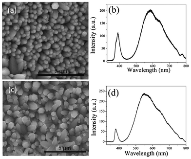 | ||
| Fig. 6 (a) SEM micrograph of the recovered sample after annealing at 500 °C and (b) the PL spectrum of the exfoliated film after annealing. (c) SEM micrograph and (d) the PL spectrum of the as-synthesized ZnO. | ||
Conclusions
Reuse reduces the consumption of fresh raw materials, waste disposal, energy usage, air pollution, water pollution, and greenhouse gas emissions, etc. It has been shown that materials that are extensively used, such as ITO and Si, can be used several times for nanoresearch without altering their material properties. The deposited materials, especially oxides, can be exfoliated by PEDOT:PSS and hybrid structures are obtained. Furthermore, the oxide materials can be recovered from the hybrid structures upon annealing at a moderate temperature. It is believed that this work will motivate researchers to find more efficient ways to retrieve the substrates even after several uses.Experimental section
Oxides such as ZnO, NiO and Cu2O films were prepared by the electrochemical method. All chemicals are used as received without any further purification. Deionized (DI) water is used in all the experiments. In a typical synthesis process, an equimolar 100 ml solution of the precursors such as hydrated zinc nitrate [Zn(NO2)3·6H2O] and hexamethylene tetramine [(CH2)6N4, HMT] for the synthesis of ZnO nanorods, nickel sulphate hexahydrate (NiSO4·6H2O) and copper sulphate (CuSO4·5H2O) for NiO and Cu2O nanostructures, are used. The experimental set up comprises of a graphite counter electrode and an ITO working electrode. The ZnO films are deposited under potentiostatic conditions at a voltage of 3 V. The electrolytic bath is maintained at 95 °C. The as-synthesized film is washed several times to get rid of the electrolyte and unwanted products. After the film is dried, a drop of PEDOT:PSS is put on the region of the ZnO film and then dried under a tungsten lamp. As the polymer becomes dry the ZnO nanorods starts to exfoliate from the substrate.Acknowledgements
The authors acknowledge financial support from the Department of Information Technology (DIT) through the Nanotechnology programme.References
- http://www.nanocs.com/ITO.htm .
- R. B. Gordon, M. Bertram and T. E. Graedel, Proc. Natl. Acad. Sci. U. S. A., 2006, 103, 1209–1214 CrossRef CAS.
- B. Thestrup and J. Schou, Appl. Phys. A: Mater. Sci. Process., 1999, 69, S807–S810 CrossRef CAS.
- W.-H. Baek, M. Choi, T.-S. Yoon, H. H. Lee and Y.-S. Kim, Appl. Phys. Lett., 2010, 96, 133503 CrossRef.
- Z. Wu, Z. Chen, X. Du, J. M. Logan, J. Sippel, M. Nikolou, K. Kamaras, J. R. Reynolds, D. B. Tanner, A. F. Hebard and A. G. Rinzler, Science, 2004, 305, 1273–1276 CrossRef CAS.
- X. Wang, L. Zhi and K. Mullen, Nano Lett., 2008, 8, 323–327 CrossRef CAS.
- S. Wu, Z. Yin, Q. He, X. Huang, X. Zhou and H. Zhang, J. Phys. Chem. C, 2010, 114, 11816–11821 CAS.
- R. B. Pode, C. J. Lee, D. G. Moon and J. I. Han, Appl. Phys. Lett., 2004, 84, 4614 CrossRef CAS.
- K. Tvingstedt and O. Inganäs, Adv. Mater., 2007, 19, 2893–2897 CrossRef CAS.
- P. B. Catrysse and S. Fan, Nano Lett., 2010, 10, 2944–2949 CrossRef CAS.
- K. Fehse, K. Walzer, K. Leo, W. Lövenich and A. Elschner, Adv. Mater., 2007, 19, 441–444 CrossRef CAS.
- Y. Zhou, F. Zhang, K. Tvingstedt, S. Barrau, F. Li, W. Tian and O. Inganas, Appl. Phys. Lett., 2008, 92, 233303 CrossRef.
- R. Konenkamp, R. C. Word and C. Schlegel, Appl. Phys. Lett., 2004, 85, 6004 CrossRef CAS.
- A. Nadarajah, R. C. Word, J. Meiss and R. Konenkamp, Nano Lett., 2008, 8, 534–537 CrossRef CAS.
- T. Zhang, Z. Xu, D. L. Tao, F. Teng, F. S. Li, M. J. Zheng and X. R. Xu, Nanotechnology, 2005, 16, 2861 CrossRef CAS.
- S. Brahma, K. Jagannatha Rao and S. Shivashankar, Bull. Mater. Sci., 2010, 33, 89–95 CrossRef CAS.
- J. Liu, S. Wang, Z. Bian, M. Shan and C. Huang, Appl. Phys. Lett., 2009, 94, 173103 CrossRef.
- E. Neshataeva, T. Kummell, G. Bacher and A. Ebbers, Appl. Phys. Lett., 2009, 94, 091113 CrossRef.
- M. L. Lee, P.-F. Chi and J. K. Sheu, Appl. Phys. Lett., 2009, 94, 013512 CrossRef.
- A. Shetty and K. K. Nanda, Appl. Phys. Lett., 2012, 100, 242108 CrossRef.
Footnote |
| † Electronic Supplementary Information (ESI) available. See DOI: 10.1039/c2ra21987e |
| This journal is © The Royal Society of Chemistry 2012 |