Rapid nanopatterning of zirconium dioxide via nanoprinting and microwave-assisted annealing†
Dae-Geun
Choi
*ab,
Ki-Joong
Lee
a,
Sarah
Kim
a,
Eung-Sug
Lee
a,
Jun-Ho
Jeong
a,
Jihye
Lee
a and
Jun-Hyuk
Choi
a
aNanomechanical System Research Division, Korea Institute of Machinery and Materials, 171 Jang-dong Yuseong-gu, Daejeon, 305-343, Republic of Korea. E-mail: lamdg@kimm.re.kr
bDepartment of Nano-Mechatronics, University of Science and Technology, 217 Gajungro Yuseong-gu, Daejeon, 305-350, Republic of Korea
First published on 14th September 2012
Abstract
High resolution nanopatterning of metal oxide materials using low cost and high throughput processes is necessary for the ongoing development of electronic and optical devices. In this work, we demonstrate the fabrication of a sub-50 nm ZrO2 nanomesh structure by size reduction induced volume shrinkage that accompanies microwave-assisted annealing. The effect of microwave annealing time on pattern dimension variations such as hole size, wall thickness, and pattern depth is investigated. The evolution of the crystallinity as well as the optical properties of the ZrO2 thin films, including the refractive index and transmittance, are studied as a function of annealing time. Interestingly, the pure tetragonal crystalline phase of ZrO2 can be obtained within minutes by rapid microwave-assisted annealing. We believe that the nanopatterning of inorganic oxide materials using the size reduction effect and rapid crystallization capability of microwave annealing is very useful in the field of nanoscale patterning and for applications involving nanoscale oxide materials.
Introduction
Metal oxide materials have been extensively investigated for various applications including solar cells, photocatalysts, thin film transistors, transparent electrodes, sensors, and other optical devices, as such materials can simultaneously exhibit high transparency, excellent electrical properties, as well as the possibility of solution processing.1–3Nanopatterning of functional metal oxide materials such as ZnO, TiO2, SnO2, SiO2, and ZrO2 has recently gained increasing interest owing to the possibility of device performance enhancement as well as further device miniaturization facilitated by the use of nanoscale elements.4–11
Owing to their low-cost and high-throughput capabilities, micro- and nanofabrication processes of oxide materials by spin-coating or inkjet printing are particularly attractive for use in device fabrication. However, high temperature annealing following solution deposition to convert an amorphous inorganic–organic hybrid oxide to a dense crystalline phase inorganic oxide material is typically required to achieve the desired high-performance material. This annealing process increases fabrication costs and prevents the use of polymeric or soft substrates. The development of high quality metal oxide materials using a rapid low temperature process is therefore warranted for a number of device applications.12–14
Although unconventional techniques such as electrochemical lithography, nanoimprint lithography (NIL), and nanomolding have been applied to metal oxide nanopatterning because of their simplicity, low-cost, and sub-50 nm resolution,5–10,15 the additional unfavorable high temperature annealing process described above is almost always required for crystallization of the metal oxide. For example, temperatures in excess of 400 °C were necessary to generate nanopatterns of crystalline anatase TiO2 and tetragonal ZrO2.8,10 We herein report the rapid nanopatterning of crystalline ZrO2 using microwave-assisted annealing (MAA) as opposed to conventional convection annealing. In our previous work, we demonstrated facile nanopatterning of ZrO2 using direct UV NIL that was subsequently crystallized by high temperature annealing, including slow heating and cooling processes.10 Crystalline ZrO2 is relevant to a number of applications owing to its high refractive index, large optical band gap, and strong thermal-, chemical-, and wear-resistance.10,16 In this work, we present the fabrication of tetragonal ZrO2 nanopatterns that can be annealed within 3 min. In addition, we demonstrate the successful fabrication of a nanomesh structure with a wall thickness of 40 nm by a convenient one-step MAA process. Finally, the effect of MAA time on the crystallinity as well as the optical properties, such as refractive index and transmittance, of the ZrO2 structures is also investigated.
Experimental
Fabrication of ZrO2 nanopattern
A silicon (Si) master consisting of hexagonal arrays with holes of 265 nm diameter and 400 nm pitch was first prepared. Flexible perfluoropolyether (PFPE) polymer mold (Young Chang Chemical) was then replicated from the Si master by UV curing with 365 nm light at an intensity of 30 mW cm−2 for a duration of 120 s. Zirconyl 2-ethylhexanoate (Strem Chemicals Inc., 6% Zr in Stoddard solvent), which serves as the ZrO2 precursor, was then spin-coated onto the polymer molds at a spin-rate of 3000 rpm for 30 s. The oxide precursor was transfer printed onto an air plasma treated p-Si(100) wafer at a temperature of 150 °C and a pressure of 6 bar for a duration of 15 min. To prepare a flat ZrO2 film, zirconyl 2-ethylhexanoate was directly spin-coated at a spin-rate of 3000 rpm onto an air plasma treated Si surface. The generated films (both patterned and unpatterned) were then subjected to microwave-assisted annealing using a commercial microwave oven (LG electronics) operating at a frequency of 2.45 GHz and a power of 700 W.Characterization methods
The thickness and refractive index of the ZrO2 films were measured by spectroscopic ellipsometry (Model M2000D, Woollam) at an incidence angle of 70°. The crystallinity of the microwave-annealed ZrO2 films was investigated by X-ray diffraction using a Rigaku D/Max 2500 diffractometer with Cu-Kα radiation (λ = 1.54178 Å) operating at 40 kV and 300 mA. Film transmittance was determined by UV-Vis spectroscopy and the nanostructured patterns were imaged by field emission scanning electron microscopy (FE-SEM).Results and discussion
A schematic describing the nanopatterning of ZrO2 using microwave-assisted annealing is depicted in Fig. 1. To generate the desired ZrO2 structures, a zirconyl 2-ethylhexanoate precursor film was first spin-coated at a spin-rate of 3000 rpm for 30 s onto p-Si(100) wafers. The films were then thermally cured at 150 °C for 15 min to solidify the precursor resin. The curing mechanism of zirconyl 2-ethylhexanoate is similar to that described in our previous work, the only difference being that thermal curing rather than UV curing was employed.10 The overall reaction mechanism can be summarized by eqn (1). | (1) |
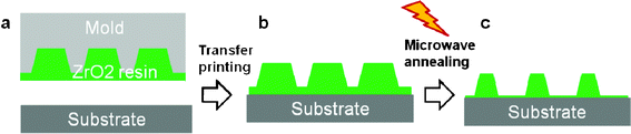 | ||
| Fig. 1 Scheme depicting the direct nanopatterning of ZrO2 by microwave-assisted annealing. | ||
The cured films were then annealed in a microwave oven (2.45 GHz frequency) for varying amounts of time. XRD spectra of the ZrO2 films were collected at various microwave annealing times, as shown in Fig. 2. A reference ZrO2 film that was subjected to only thermal curing at 150 °C was found to be completely amorphous (reference in Fig. 2a). Using conventional thermal annealing, the ZrO2 crystalline phase typically appears with treatment at temperatures exceeding 400 °C for a lengthy period of time.10 In our MAA process, amorphous ZrO2 structures were readily converted to crystalline tetragonal ZrO2 after 60 s of treatment. Within 180 s of MAA processing, the (111), (200), (220), and (311) diffraction peaks expected for crystalline ZrO2 had all appeared.
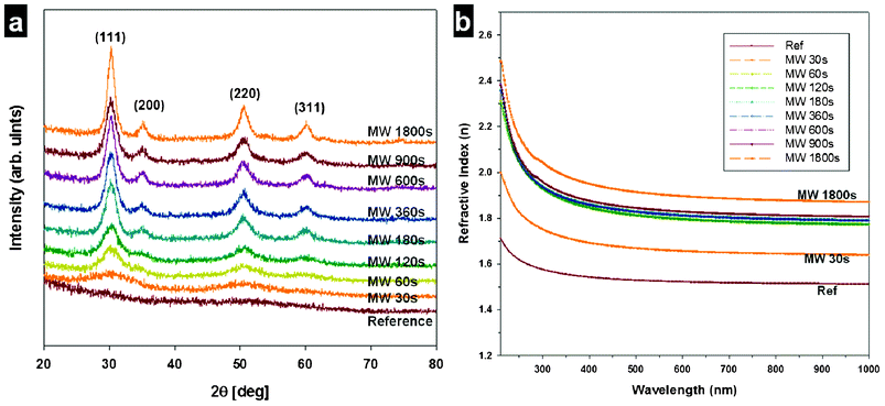 | ||
| Fig. 2 (a) XRD of the ZrO2 films as a function of microwave annealing time. (b) Dispersion relations for ZrO2 films microwave annealed for different amounts of time. | ||
The dispersion relation (i.e., refractive index (n) as a function of wavelength) of ZrO2 films treated with MMA to varying extents is shown in Fig. 2b. The refractive indices at 500 nm were 1.53, 1.67, 1.82, 1.82, 1.83, 1.83, 1.85, 1.85, and 1.92 for the ZrO2 films treated for a duration of 0, 30, 60, 120, 180, 300, 600, 900, and 1800 s by MAA, respectively. The film thickness, as determined by spectroscopic ellipsometry, was reduced from 850 nm to 452 nm as the MAA exposure time was increased from 0 to 1800 s (Table 1).
| Annealing @ 150 °C for 15 min | MW 60 s | MW 180 s | MW 600 s | MW 1800 s | ||
|---|---|---|---|---|---|---|
| Feature size (400 nm pitch) | Hole size (nm) | 288 | 340 (18% increase) | 345 (20% increase) | 360 (25% increase) | — |
| Wall width (nm) | 122 | 60 (51% reduction) | 55 (55% reduction) | 40 (67% reduction) | — | |
| Pattern depth (nm) | 356 | 175 (51% reduction) | 131 (63% reduction) | 73 (80% reduction) | — | |
| Refractive index @ 500 nm | 1.53 | 1.82 | 1.83 | 1.85 | 1.92 | |
| Film thickness (nm) | 850 | 544 | 492 | 471 | 452 | |
There are many reports describing the use of microwave sintering in the synthesis of metal oxide particles as well as thin films.1,14,17–25 A systematic study of the effect of microwave treatment in the fabrication of nanopatterned metal oxide materials is currently lacking, however. It is important that variations in pattern dimensions and material optical properties with changing MAA processing times are characterized (Fig. 3 and Table 1). The hole size of the patterned ZrO2 after transfer printing at 150 °C for 15 min was 288 nm, which is slightly larger than the 265 nm holes of the silicon master (Fig. 3a and 3d, Table 1). As MAA times were increased from 0 to 600 s, the hole size increased from 288 nm to 360 nm. Meanwhile, wall-width decreased from 122 nm to 40 nm (Fig. 3a–c) and pattern depth decreased from 356 nm to 73 nm (Fig. 3d–f) (see also Table 1). Interestingly, a nanomesh structure with sub-50 nm feature sizes could be successfully fabricated by means of the size reduction induced by MAA, as shown in Fig. 3c. Volume shrinkage originated from decomposition of the organic molecules present as well as the structural rearrangement that accompanies the amorphous to crystalline phase transition.10 Compared with the as-prepared amorphous ZrO2 pattern, pattern width and pattern depth were reduced by 67% and 80%, respectively, as shown in Fig. 3 and Table 1. From our results, it is anticipated that the size reduction method observed for MAA will be increasingly employed with low-cost masters for use in nanopatterning,9 although there are previous reports using other approaches such as lithographically controlled wetting to reduce the size of the pattered feature compared to the size of the stamp.26–29
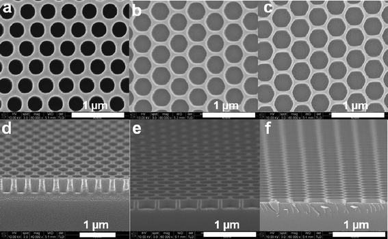 | ||
| Fig. 3 SEM images of ZrO2 nanostructures (a) just after transfer printing, (b) after 60 s of microwave annealing, and (c) after 600 s of microwave annealing. SEM images (d–f) are cross-section images of (a-c), respectively. | ||
UV-vis spectroscopy was employed to evaluate the transmittance of the ZrO2 film nanopatterns following microwave annealing (Fig. 4). The transmittance at 600 nm of the reference ZrO2 film, the ZrO2 film treated with MAA for 600 s, and the ZrO2 nanopattern treated with MAA for 600 s was 99%, 93%, and 98%, respectively. The slight decrease in transmittance for the MMA treated ZrO2 film may be attributed to the formation of a dense crystalline phase, as confirmed by an increase in the refractive index. The transmittance spectrum of the ZrO2 nanopattern treated with MAA for 600 s displays two spectral regions, as shown in Fig. 4. Transmittance at wavelengths greater than 540 nm increased to 98%, because the nanopattern has a transparent window area matching the nanopattern hole size, as well as the antireflection effect of the nanopattern which reduces total reflection losses due to surface scattering.30 Severe transmittance reduction for wavelengths between 400 and 530 nm can be attributed to Bragg reflections from the periodic nanopattern of 400 nm pitch. The position of the stop-band of the ordered structure can be approximated by Bragg's diffraction law, nλ = 2dsinθ, where λ, d, and θ correspond to the wavelength of the maximum reflection peak, atomic lattice spacing, and the angle of incidence, respectively. The position of maximum reflection loss depends strongly on the internal lattice spacing (d) of the nanopattern. Therefore, various patterns with sub-300 nm pitch are generally used for antireflection purposes over the visible wavelength range.31
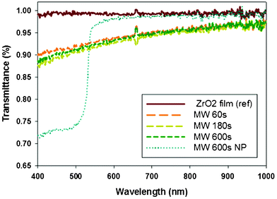 | ||
| Fig. 4 Transmittance of ZrO2 films and a ZrO2 nanopattern following microwave annealing. | ||
Conclusions
In summary, we have demonstrated the rapid fabrication of nanopatterned crystalline ZrO2 films using nanotransfer printing and microwave annealing. Conversion of the amorphous ZrO2 structures to their corresponding tetragonal crystalline phase appeared upon 60 s of MMA exposure. The pure tetragonal crystalline phase formed within 180 s of MMA treatment. The refractive index of the amorphous ZrO2 film increased from 1.53 to 1.92 following MAA. The optical transmittance of the ZrO2 thin films and nanopatterns was also investigated as a function of the duration of MAA treatment. Finally, the effect of MAA processing on the nanopattern dimensions was also considered and, interestingly, allowed for the successful fabrication of a nanomesh structure with sub-50 nm wall thickness. We believe that the simplicity of this size reduction method will be useful in the further development of nanoscale patterning, which will impact a number of technologies.Acknowledgements
This research was supported by KIMM research funds (NK169D and SC0890), NRF grants (No.2011-0028585 and 2011-0031563), and a National Platform Technology grant (10033636).References
- G. R. Patzke, Y. Zhou, R. Kontic and F. Conrad, Angew. Chem., Int. Ed., 2011, 50, 826–859 CrossRef CAS.
- T. Kamiya and H. Hosono, NPG Asia Mater., 2010, 2, 15–22 CrossRef.
- J. W. Reiner, A. M. Kolpak, Y. Segal, K. F. Garrity, S. Ismail-Beigi, C. H. Ahn and F. J. Walker, Adv. Mater., 2010, 22, 2919–2938 CrossRef CAS.
- C. Battaglia, J. Escarré, K. Söderström, M. Charrière, M. Despeisse, F. J. Haug and C. Ballif, Nat. Photonics, 2011, 5, 535–538 CrossRef CAS.
- S. H. Lim, M. S. M. Saifullah, H. Hussain, W. W. Loh and H. Y. Low, Nanotechnology, 2010, 21, 285303 CrossRef.
- K. m. Yoon, K. y. Yang and H. Lee, Thin Solid Films, 2009, 518, 126–129 CrossRef CAS.
- H. H. Park, D. G. Choi, X. Zhang, S. Jeon, S. J. Park, S. W. Lee, S. Kim, K. D. Kim, J. H. Choi, J. Lee, D. K. Yun, K. J. Lee, R. H. Hill and J. H. Jeong, J. Mater. Chem., 2010, 20, 1921–1926 RSC.
- R. Ganesan, J. Dumond, M. S. M. Saifullah, S. H. Lim, H. Hussain and H. Y. Low, ACS Nano, 2012, 6, 1494–1502 CrossRef CAS.
- H. H. Park, W. L. Law, X. Zhang, S. Y. Hwang, S. H. Jung, H. B. Shin, H. K. Kang, R. H. Hill and C. K. Ko, ACS Appl. Mater. Interfaces, 2012, 4, 2507–2514 CAS.
- H. H. Park, X. Zhang, S. W. Lee, K. D. Kim, D. G. Choi, J. H. Choi, J. Lee, E. S. Lee, R. H. Hill and J. H. Jeong, J. Mater. Chem., 2011, 21, 657–662 RSC.
- M. Cavallini, Z. Hemmatian, A. Riminucci, M. Prezioso, V. Morandi and M. Murgia, Adv. Mater., 2012, 24, 1197–1201 CrossRef CAS.
- K. K. Banger, Y. Yamashita, K. Mori, R. L. Peterson, T. Leedham, J. Rickard and H. Sirringhaus, Nat. Mater., 2011, 10, 45–50 CrossRef CAS.
- K. M. Kim, C. W. Kim, J. S. Heo, H. Na, J. E. Lee, C. B. Park, J. U. Bae, C. D. Kim, M. Jun, Y. K. Hwang, S. T. Meyers, A. Grenville and D. A. Keszler, Appl. Phys. Lett., 2011, 99 Search PubMed.
- S. Jeong and J. Moon, J. Mater. Chem., 2012, 22, 1243–1250 RSC.
- F. C. Simeone, C. Albonetti and M. Cavallini, J. Phys. Chem. C, 2009, 113, 18987–18994 CAS.
- L. Kumari, W. Z. Li, J. M. Xu, R. M. Leblanc, D. Z. Wang, Y. Li, H. Guo and J. Zhang, Cryst. Growth Des., 2009, 9, 3874–3880 CAS.
- T. Jun, K. Song, Y. Jeong, K. Woo, D. Kim, C. Bae and J. Moon, J. Mater. Chem., 2011, 21, 1102–1108 RSC.
- K. Song, Y. K. Chang, T. Jun, D. Lee, Y. Jeong and J. Moon, J. Cryst. Growth, 2011, 326, 23–27 CrossRef CAS.
- Y. V. Bykov, K. I. Rybakov and V. E. Semenov, J. Phys. D: Appl. Phys., 2001, 34, R55–R75 CrossRef CAS.
- K. E. Haque, Int. J. Miner. Process., 1999, 57, 1–24 CrossRef CAS.
- E. T. Thostenson and T. W. Chou, Composites, Part A, 1999, 30, 1055–1071 CrossRef.
- M. Oghbaei and O. Mirzaee, J. Alloys Compd., 2010, 494, 175–189 CrossRef CAS.
- J. N. Hart, D. Menzies, Y. B. Cheng, G. P. Simon and L. Spiccia, Sol. Energy Mater. Sol. Cells, 2007, 91, 6–16 CrossRef CAS.
- G. A. Tompsett, W. C. Conner and K. S. Yngvesson, ChemPhysChem, 2006, 7, 296–319 CrossRef CAS.
- J. Liang, Z. Deng, X. Jiang, F. Li and Y. Li, Inorg. Chem., 2002, 41, 3602–3604 CrossRef CAS.
- M. Cavallini, D. Gentili, P. Greco, F. Valle and F. Biscarini, Nat. Protoc., 2012, 7, 1668–1676 CrossRef CAS.
- E. Coronado, C. Martí-Gastaldo, J. R. Galán-Mascarós and M. Cavallini, J. Am. Chem. Soc., 2010, 132, 5456–5468 CrossRef CAS.
- P. Greco, M. Cavallini, P. Stoliar, S. D. Quiroga, S. Dutta, S. Zacchini, M. C. Iapalucci, V. Morandi, S. Milita, P. G. Merli and F. Biscarini, J. Am. Chem. Soc., 2008, 130, 1177–1182 CrossRef CAS.
- M. Cavallini, J. Mater. Chem., 2009, 19, 6085–6092 RSC.
- K. J. Lee, J. H. Jeong, K. D. Kim, J. Lee and D. G. Choi, J. Korean Phys. Soc., 2009, 55, 566–571 CrossRef CAS.
- B. Päivänranta, N. Heikkila and M. Kuittinen, J. Opt. Soc. Am. A, 2007, 24, 1680–1686 CrossRef.
Footnote |
| † Electronic Supplementary Information (ESI) available. See DOI: 10.1039/c2ra21919k |
| This journal is © The Royal Society of Chemistry 2012 |