Synthesis and characterization of few-layer Sb2Te3 nanoplates with electrostatic properties
Guolin
Hao
a,
Xiang
Qi
a,
Guang
Wang
b,
Xiangyang
Peng
a,
Shengli
Chang
b,
Xiaolin
Wei
a and
Jianxin
Zhong
*a
aHunan Provincial Key Laboratory of Micro-Nano Energy Materials and Devices, Laboratory for Quantum Engineering and Micro-Nano Energy Technology and Faculty of Materials and Optoelectronic Physics, Xiangtan University, Hunan 411105, P. R. China. E-mail: jxzhong@xtu.edu.cn; Fax: +86 0731-58298612; Tel: +86 0731-58293749
bCenter of Material Science, College of Science, National University of Defense Technology, Changsha 410073, P. R. China
First published on 17th September 2012
Abstract
Sb2Te3-based nanomaterials are predicted to be one of the topological insulators promising in future spintronics and topological quantum computation. Few-layer Sb2Te3 nanoplates on different substrates forming heterostructures were fabricated via the vapor phase deposition method. The electrostatic properties of Sb2Te3 nanoplates were characterized by Kelvin probe force microscopy. It was found that Sb2Te3 nanoplates exhibit uniform surface potential and charge distribution. The work function was determined to be ∼5.016 eV for Sb2Te3 nanoplates grown on highly oriented pyrolytic graphite. These results pave a route to explore the exotic topological properties of Sb2Te3-based nanoelectronic devices.
1. Introduction
Antimony telluride (Sb2Te3) is one of the layered narrow band gap semiconductors with rhombohedral structure, which has been employed as the best candidate for near room-temperature thermoelectric applications.1,2 Recently, both theoretical and experimental investigations have demonstrated that Sb2Te3, Bi2Te3 and Bi2Se3 are topological insulators (TIs) with a gapped insulator in the bulk but possessing gapless surface states protected by time-reversal symmetry on the surface,1,3–14 which have promising applications in spintronics and topological quantum computation.15,16 Therefore, growth of high quality TI Sb2Te3 is crucial for its realistic applications.17,18 Successful growth of Sb2Te3 on different substrates would further promote developments in topological insulator material engineering and integration.Low-dimensional Sb2Te3 materials exhibiting extremely large surface-to-volume ratios are essential for the transport properties associated with topological surface states.2,4 Sb2Te3 nanostructures have been prepared by employing various methods such as molecular beam epitaxy,17 solvothermal process,19 “graphene-like” exfoliation,20 and vapor–liquid–solid process.21 In this paper, few-layer Sb2Te3 nanoplates with various morphologies have been successfully synthesized on different substrates forming heterostructures by vapor phase deposition method, which doesn’t need any catalysts compared to other methods in fabricating nanomaterials.22–26
In previous reports, Sb2Te3 samples were characterized by angle-resolved photoemission spectroscopy as well as scanning tunneling microscopy. It was shown that Fermi energies of Sb2Te3 lie in the band gap of the bulk, intersecting the Dirac cone of the surface states.1,8,11,17 However, promising applications of Sb2Te3 require the films to rest on different substrates forming heterostructures, and few experiments of the electrostatic properties of Sb2Te3 are directly probed. Herein, the surface potential and charge distribution of Sb2Te3 nanoplates (NPs) were investigated by Kelvin probe force microscopy (KPFM) technique, based on dynamic force microscopy principles, which has its own advantages for imaging heterogeneous surfaces and can give much information on topography and potential distribution of the sample with high spatial resolution.27–30 Moreover, the work function of Sb2Te3 NPs resting on highly oriented pyrolytic graphite (HOPG) was determined. These results could provide a framework for designing Sb2Te3 nanoplate-based devices.
2. Experimental details
2.1 Synthesis of Sb2Te3 nanostructures
Similar to Bi2Te3 and Bi2Se3, Sb2Te3 has a rhombohedral crystal structure belonging to the space group D53d (R![[3 with combining macron]](https://www.rsc.org/images/entities/char_0033_0304.gif) m), consisting of five-atom layers arranged along the z axis known as quintuple layers (QLs) shown in Fig. 1a. Covalently bonded quintuple layers are held together predominantly by weak van der Waals interactions. Few-layer Sb2Te3 NPs with various nanostructures on SiO2/Si (300 nm), Si (111), HOPG, and mica substrates have been synthesized in a 12 inch horizontal tube furnace at a temperature of 510 °C by catalyst-free vapor phase deposition method as schematically shown in Fig. 1b. The source material, 0.5 g of Sb2Te3 powders (99.999%), is used as precursors and placed in the hot center of the furnace. Various wafers are located at the downstream zone (10–12 cm away from the centre) as growth substrates. Before synthesis, the tube is flushed 5 times with high-purity Ar gas to decrease oxygen contamination. An inert environment is maintained with a flow rate of 100 sccm Ar and the temperature in the hot center of furnace is heated to 510 °C at the given rate under the various pressures ranging from 10 mTorr to 30 Torr during the growth. The reaction time is maintained for 5 min under these conditions and then cooled down to room temperature naturally.
m), consisting of five-atom layers arranged along the z axis known as quintuple layers (QLs) shown in Fig. 1a. Covalently bonded quintuple layers are held together predominantly by weak van der Waals interactions. Few-layer Sb2Te3 NPs with various nanostructures on SiO2/Si (300 nm), Si (111), HOPG, and mica substrates have been synthesized in a 12 inch horizontal tube furnace at a temperature of 510 °C by catalyst-free vapor phase deposition method as schematically shown in Fig. 1b. The source material, 0.5 g of Sb2Te3 powders (99.999%), is used as precursors and placed in the hot center of the furnace. Various wafers are located at the downstream zone (10–12 cm away from the centre) as growth substrates. Before synthesis, the tube is flushed 5 times with high-purity Ar gas to decrease oxygen contamination. An inert environment is maintained with a flow rate of 100 sccm Ar and the temperature in the hot center of furnace is heated to 510 °C at the given rate under the various pressures ranging from 10 mTorr to 30 Torr during the growth. The reaction time is maintained for 5 min under these conditions and then cooled down to room temperature naturally.
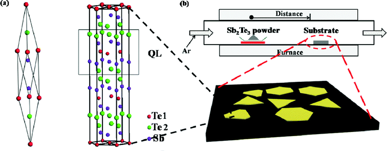 | ||
| Fig. 1 (a) The rhombohedral primitive and the hexagonal unit cells of Sb2Te3 with quintuple layers along the c axis. (b) Experimental setup of the furnace employed for the synthesis of Sb2Te3 NPs. | ||
2.2 Characterization
The crystal structures of the as-synthesized Sb2Te3 NPs are determined by X-ray diffraction (XRD) (Rigaku D/MAX-2500, Cu Kα radiation). The morphologies and microstructures of the samples are characterized employing optical microscopy, scanning electron microscopy (SEM, JEOL, JSM-6360), high-resolution transmission electron microscopy (TEM, JEM2100) equipped with an energy dispersive X-ray spectrometer (EDS), and atomic force microscopy (AFM, SEIKO, SPI3800N + 300 HV). The electrostatic properties of Sb2Te3 NPs are performed by KPFM (AFM, SEIKO, SPI3800N + 300 HV) employing a dual-pass mode in traditional tapping atomic force microscopy under ambient conditions with humidity of ∼40%.3. Results and discussions
3.1 Characterizations of Sb2Te3 nanostructures
An XRD pattern of as-prepared products is shown in Fig. 2. Sb2Te3 NPs are obtained on the SiO2/Si (300 nm) substrates with a temperature in the hot center of 510 °C reached with a heating rate of 17 °C min−1 under a pressure of 10 mTorr during the growth process. All peaks can be perfectly indexed to rhombohedral Sb2Te3 (JCPDS: 15-0874), which are in good agreement with the lattice parameters of a = 0.4262 nm and c = 3.045 nm. This result demonstrates that pure phase Sb2Te3 is synthesized via the vapor phase deposition method.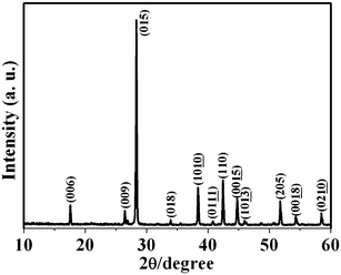 | ||
| Fig. 2 XRD pattern of as-prepared Sb2Te3 NPs. | ||
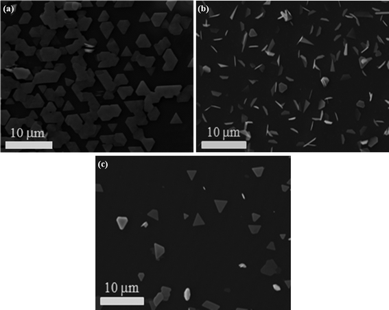
The morphologies of Sb2Te3 are characterized by SEM. Fig. 3a and b show that the synthesized products are predominantly hexagonal-based NPs connected to each other, exhibiting well-defined shape and uniform size. During the synthesis process, it is found that two essential parameters, i.e. heating rate and pressure, in the vapor phase deposition system have vital influence on the growth of Sb2Te3 NPs. When the pressure varies from 10 mTorr to 30 Torr with the other parameters fixed compared to synthesis conditions of the products as shown in Fig. 3a and b, the Sb2Te3 NPs with linear arrangement are oriented in the direction perpendicular to the flat substrate surface with the c axis parallel to the surface plane (Fig. 3c and d). The lateral dimension of Sb2Te3 NPs is about 2.5 μm. When the heating rate is improved to be 64 °C min−1 under a pressure of 30 Torr, one can see that Sb2Te3 NPs are grown lying on the substrate. It is interesting to note that the edge length (∼8 μm) increases significantly with the heating rate of 64 °C min−1 up to a temperature of 510 °C (Fig. 3e). The corresponding XRD pattern is shown in Fig. 3f. The dominant (006) and (0015) diffraction peaks suggest that the as-prepared Bi2Te3 NPs have a preferred orientation along the (00l) direction under the growth condition indicating that the (00l) facets have lower surface energies. Therefore, the growth along the c-axis vertical to the surface of Sb2Te3 NP is faster than that along the lateral surface, which has been confirmed for Bi2Te3 and Bi2Se3 NPs in previous reports;31–33 therefore Sb2Te3 NPs are successfully prepared. At a heating rate of 17 °C min−1, we propose that the speed of bismuth and antimony atoms reaching the substrate is so slow that the Sb2Te3 NPs are grown in the vertical direction of substrate, while, at the heating rate of 64 °C min−1, bismuth and antimony atoms reaching the substrate are very active and move quickly to the edge of the Sb2Te3 NPs.
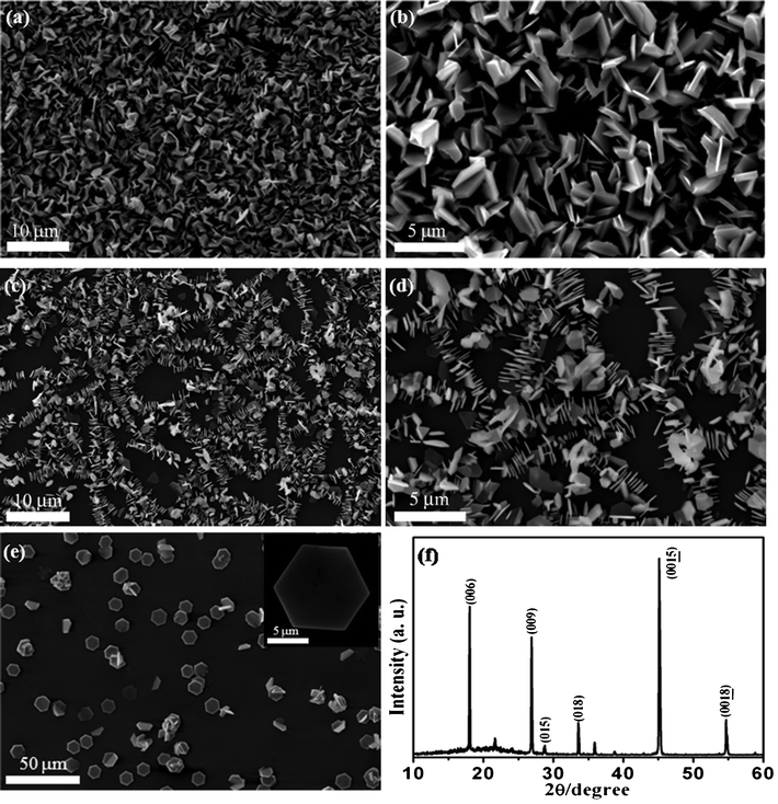 | ||
| Fig. 3 (a)–(b) SEM images of Sb2Te3 NPs obtained on SiO2/Si (300 nm) substrates under 10 mTorr at a heating rate of 17 °C min−1. (c)–(d) SEM images of as-grown Sb2Te3 NPs under 30 Torr at a heating rate of 17 °C min−1. (e) SEM image of Sb2Te3 NPs under 30 Torr at a heating rate of 64 °C min−1. Inset: high-magnification image of a Sb2Te3 NP. (f) Corresponding XRD pattern of as-prepared products as shown in (e). | ||
The composition and structure of Sb2Te3 NPs are further studied using EDS and TEM. A typical TEM image of a Sb2Te3 NP is shown in Fig. 4a. The high resolution TEM images taken from the NP with clear lattice fringes and corresponding fast Fourier transformation (FFT) further confirm the single-crystalline nature of Sb2Te3 NP as shown in Fig. 4b. The corresponding stoichiometry between Sb and Te are 39.36% and 60.64%, respectively, which is close to the formula of Sb2Te3 (Fig. 4c). A typical optical image of Sb2Te3 NPs on the SiO2/Si (300 nm) substrates is displayed under white light illumination (Fig. 5a). Fig. 5b exhibits a typical AFM topography of Sb2Te3 NP with flat surfaces.
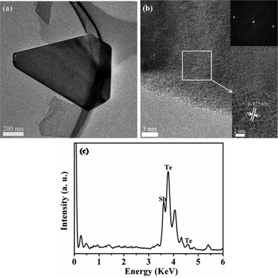 | ||
| Fig. 4 (a) TEM image of Sb2Te3 NP. (b) HRTEM image of the same Sb2Te3 NP. Inset: magnified HRTEM image and corresponding fast Fourier transformation pattern. (c) EDS spectrum taken from a single Sb2Te3 NP indicated in (a). | ||
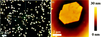 | ||
| Fig. 5 (a) Optical image of as-prepared Sb2Te3 NPs at a rate of 64 °C min−1 up to a temperature of 510 °C. (b) Topography AFM image of Sb2Te3 NPs. | ||
Currently, epitaxial growth of TI on diverse substrates is of great interest due to the properties associated with the surface state coupling at the interface. Besides the above silicon oxide substrate material, Sb2Te3 NPs are successfully grown on various substrates including mica, HOPG and Si(111) by vapor phase deposition method without any catalyst. Fig. 6a shows the SEM image of Sb2Te3 NPs prepared on mica substrate. Compared to the products obtained on HOPG and Si(111) substrates, as shown Fig. 6b and c, the Sb2Te3 NPs on mica have a certain orientation, which may further promote developments in Sb2Te3-based material engineering and integration.
 | ||
| Fig. 6 (a–c) SEM images of Sb2Te3 NPs grown on mica, HOPG and Si (111) substrates, respectively. | ||
3.2 Electrostatic properties of Sb2Te3 NPs
In recent years, much attention has been paid to the transport properties of TI-based device exploring the ideal TI properties.31,34,35 Little attention is paid to the electrostatic properties of TIs,28 which is also crucial for TI-based device and integration. We have carried out surface and charge distribution measurements using KPFM employing MikroMasch CSC-17/Cr-Au tips with a force constant of 0.15 N m−1 at a fixed tip–sample distance of ∼50 nm on HOPG under ambient environment with humidity of ∼40%. KPFM images of the sample surfaces are acquired with the cantilever vibrating at a frequency slightly lower (∼2 kHz) than its resonance frequency at a probe scan rate of 0.5 Hz.Fig. 7a is a representative topographic image of Sb2Te3 NP grown on HOPG forming a heterostructure, which exhibits smooth surface morphologies with a thickness of ∼20 nm. Fig. 7b is the corresponding surface potential image. The dark feature on the CPD (contact potential difference) map corresponds to Sb2Te3 NP exhibiting uniform surface potential and charge distribution. The darker contrast on the Sb2Te3 NP compared to HOPG substrate corresponds to a higher work function. This means that electron charges flow from HOPG into Sb2Te3 NP at the interface of Sb2Te3 NP-HOPG heterostructures. Thus, the Fermi level of Sb2Te3 NPs can be upshifted through electron diffusion, which is in accordance with previous reports.17
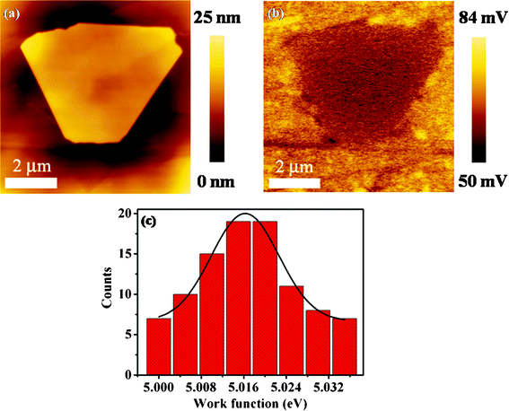 | ||
| Fig. 7 (a) Topographic image of Sb2Te3 NP grown on HOPG substrate. (b) Corresponding surface potential image of Sb2Te3 NP. (c) Statistics of work functions of Sb2Te3 NPs grown on HOPG substrates. | ||
The Sb2Te3 NP surface local work function of the sample can be calculated as follows:
| Φsample = ΦHOPG + eCPDHOPG − eCPDsample |
Φsample is the work function of sample. ΦHOPG is the work function of HOPG. CPDHOPG and CPDsample are the CPD of the HOPG and the sample, respectively. e is the elementary charge.
The work function of Ti–Pt coated tips is first calibrated with HOPG (ΦHOPG ∼5.0 eV) to convert the measured CPD to absolute surface local work function.30,36 To obtain the Sb2Te3 NP work function, a large number of NPs are characterized. Fig. 7c shows the work function statistical distribution of Sb2Te3 NPs fitted well to a Gaussian distribution with an average work function of ∼5.016 eV. The distribution of work function is narrow from 4.97 eV to 5.035 eV in the statistic, which implies that the chemical potential of Sbi2Te3 NPs possibly depends on their morphologies and thickness.
In order to investigate the dissipation of injected electrons, charge injection is achieved employing a gold-coated Si probe (SI-DF3-A) with force constant of 1.1 N m−1 by pressing the conductive tip biased at Vinj, with respect to the substrate, with a typical 2 nN contact force on a given Sb2Te3 NP. Injection experiments have been performed with a constant injection time of 2 min. Charge injection measurements indicate that both electrons and holes can be injected into the NP exhibiting ambipolar surface potential as shown in Fig. 8. The surface potential as a function of applied biases reveals an asymmetric bias dependence, suggesting that the sign of surface potential strongly rely on the completion charge trapping effect. It is interesting to note that the surface potential values after positive biases are higher than those of corresponding negative biases, indicating that electron trapping is easier than hole trapping in Sb2Te3 NP. These charge trapping maps imply the p-type nature of Sb2Te3 during growth process, which is ascribed to Sb vacancies and SbTe antisites as shown in previous reports by means of ARPES and STM.4,8,18 Our measurement provides a new way to detect the doped nature of Sb2Te3 NP through charge injection characterized by KPFM.
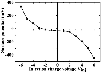 | ||
| Fig. 8 The surface potential of Sb2Te3 NP as a function of charge injection under different applied biases. | ||
4. Conclusion
In conclusion, high-quality hexagonal-based Sb2Te3 NPs have been synthesized on diverse substrates by a vapor phase deposition method without any catalyst. By employing the KPFM technique, the electrostatic properties of Sb2Te3 NPs are investigated, which shows that the surface potential is uniform and the work function on HOPG is determined to be about 5.016 eV. Moreover, charge injection measurements show that the electrons can be injected easily into the NP compared to hole injection, implying the p-doped nature of synthesized Sb2Te3 NPs. These results have important implications for exploring intriguing topological properties for Sb2Te3 NP-based devices, providing new opportunities to design TI and other effective TI-based heterostructures.Acknowledgements
This work was supported by the Grants from National Natural Science Foundation of China (Nos. 11074211, 11104347, 51172191, 51002129 and 11274265), National Basic Research Program of China (2012CB921303), the Open Fund based on the innovation platform of Hunan colleges and universities (No. 11K008), the Hunan Provincial Innovation Foundation for Graduate (No. CX2011B254) and Furong Scholar Program of Hunan Provincial Government.References
- R. Venkatasubramanian, E. Siivola, T. Colpitts and B. O'Quinn, Nature, 2001, 413, 597–602 CrossRef CAS.
- D. Hsieh, Y. Xia, D. Qian, L. Wray, F. Meier, J. H. Dil, J. Osterwalder, L. Patthey, A. V. Fedorov, H. Lin, A. Bansil, D. Grauer, Y. S. Hor, R. J. Cava and M. Z. Hasan, Phys. Rev. Lett., 2009, 103, 146401 CrossRef CAS.
- H. Zhang, C.-X. Liu, X.-L. Qi, X. Dai, Z. Fang and S.-C. Zhang, Nat. Phys., 2009, 5, 438–442 CrossRef CAS.
- G. Wang, X. Zhu, J. Wen, X. Chen, K. He, L. Wang, X. Ma, Y. Liu, X. Dai, Z. Fang, J. Jia and Q. Xue, Nano Res., 2010, 3, 874–880 CrossRef CAS.
- M. Z. Hasan and C. L. Kane, Rev. Mod. Phys., 2010, 82, 3045 CrossRef CAS.
- D. Teweldebrhan, V. Goyal and A. A. Balandin, Nano Lett., 2010, 10, 1209–1218 CrossRef CAS.
- F. Xiu, L. He, Y. Wang, L. Cheng, L.-T. Chang, M. Lang, G. Huang, X. Kou, Y. Zhou, X. Jiang, Z. Chen, J. Zou, A. Shailos and K. L. Wang, Nat. Nanotechnol., 2011, 6, 216–221 CrossRef CAS.
- D. Kong, Y. Chen, J. J. Cha, Q. Zhang, J. G. Analytis, K. Lai, Z. Liu, S. S. Hong, K. J. Koski, S.-K. Mo, Z. Hussain, I. R. Fisher, Z.-X. Shen and Y. Cui, Nat. Nanotechnol., 2011, 6, 705–709 CrossRef CAS.
- M. Z. Hossain, S. L. Rumyantsev, K. M. F. Shahil, D. Teweldebrhan, M. Shur and A. A. Balandin, ACS Nano, 2011, 5, 2657–2663 CrossRef CAS.
- Y. Wang, F. Xiu, L. Cheng, L. He, M. Lang, J. Tang, X. Kou, X. Yu, X. Jiang, Z. Chen, J. Zou and K. L. Wang, Nano Lett., 2012, 12, 1170–1175 CrossRef CAS.
- W. Shi, L. Zhou, S. Song, J. Yang and H. Zhang, Adv. Mater., 2008, 20, 1892–1897 CrossRef CAS.
- H. Peng, K. Lai, D. Kong, S. Meister, Y. Chen, X.-L. Qi, S.-C. Zhang, Z.-X. Shen and Y. Cui, Nat. Mater., 2010, 9, 225–229 CAS.
- X. L. Qi and S. C. Zhang, The quantum spin Hall effect and topological insulators, Physics Today, 2010, 63(1), 33–38 CrossRef CAS.
- A. A. Taskin, Z. Ren, S. Sasaki, K. Segawa and Y. Ando, Phys. Rev. Lett., 2011, 107, 016801 CrossRef CAS.
- J. Moore, Nat. Phys., 2009, 5, 378–380 CrossRef CAS.
- X.-L. Qi, R. Li, J. Zang and S.-C. Zhang, Science, 2009, 323, 1184–1187 CrossRef CAS.
- Y. Jiang, Y. Y. Sun, M. Chen, Y. Wang, Z. Li, C. Song, K. He, L. Wang, X. Chen, Q.-K. Xue, X. Ma and S. B. Zhang, Phys. Rev. Lett., 2012, 108, 066809 CrossRef.
- Y. Jiang, Y. Wang, M. Chen, Z. Li, C. Song, K. He, L. Wang, X. Chen, X. Ma and Q.-K. Xue, Phys. Rev. Lett., 2012, 108, 016401 CrossRef.
- R. Jin, G. Chen, J. Pei, H. Xu and Z. S. Lv, RSC Adv., 2012, 2, 1450–1456 RSC.
- K. M. F. Shahil, M. Z. Hossain, V. Goyal and A. A. Balandin, J. Appl. Phys., 2012, 111, 054305 CrossRef.
- Y. M. Zuev, J. S. Lee, C. m. Galloy, H. Park and P. Kim, Nano Lett., 2010, 10, 3037–3040 CrossRef CAS.
- P. Gehring, B. Gao, M. Burghard and K. Kern, Appl. Phys. Lett., 2012, 101, 023116 CrossRef.
- R. Venkatasubramanian, T. Colpitts, E. Watko, M. Lamvik and N. El-Masry, J. Cryst. Growth, 1997, 170, 817–821 CrossRef CAS.
- G. Z. Xing, X. S. Fang, Z. Zhang, D. D. Wang, X. Huang, J. Guo, L. Liao, Z. Zheng, H. R. Xu, T. Yu, Z. X. Shen, C. H. A. Huan, T. C. Sum, H. Zhang and T. Wu, Nanotechnology, 2010, 21, 255701 CrossRef CAS.
- D. Wang, Q. Chen, G. Xing, J. Yi, S. Rahman Bakaul, J. Ding, J. Wang and T. Wu, Nano Lett., 2012, 12, 3994–4000 CrossRef CAS.
- P. Yang, H. Yan, S. Mao, R. Russo, J. Johnson, R. Saykally, N. Morris, J. Pham, R. He and H. J. Choi, Adv. Funct. Mater., 2002, 12, 323–331 CrossRef CAS.
- Y. Shi, K. K. Kim, A. Reina, M. Hofmann, L.-J. Li and J. Kong, ACS Nano, 2010, 4, 2689–2694 CrossRef CAS.
- G. L. Hao, X. Qi, L. W. Yang, Y. D. Liu, J. Li, L. Ren, F. Sun and J. X. Zhong, AIP Adv., 2012, 2, 012114 CrossRef.
- Y. Shi, X. Dong, P. Chen, J. Wang and L.-J. Li, Phys. Rev. B: Condens. Matter Mater. Phys., 2009, 79, 115402 CrossRef.
- G. L. Hao, X. Qi, L. W. Yang, Z. Y. Huang, C. Y. Cai, L. Xue, S. X. Yu and J. X. Zhong, Solid State Commun., 2012 DOI:10.1016/j.ssc.2012.08.018.
- D. Kong, W. Dang, J. J. Cha, H. Li, S. Meister, H. Peng, Z. Liu and Y. Cui, Nano Lett., 2010, 10, 2245–2250 CrossRef CAS.
- J. J. Cha, D. Kong, S.-S. Hong, J. G. Analytis, K. Lai and Y. Cui, Nano Lett., 2012, 12, 1107–1111 CrossRef CAS.
- G. L. Hao, X. Qi, Y. D. Liu, Z. Y. Huang, H. X. Li, K. Huang, J. Li, L. W. Yang and J. X. Zhong, J. Appl. Phys., 2012, 111, 114312 CrossRef.
- Z. Ren, A. A. Taskin, S. Sasaki, K. Segawa and Y. Ando, Phys. Rev. B: Condens. Matter Mater. Phys., 2011, 84, 075316 CrossRef.
- Z. Ren, A. A. Taskin, S. Sasaki, K. Segawa and Y. Ando, Phys. Rev. B: Condens. Matter Mater. Phys., 2011, 84, 165311 CrossRef.
- J. B. Cui, J. Ristein and L. Ley, Phys. Rev. B: Condens. Matter, 1999, 60, 16135–16142 CrossRef CAS.
| This journal is © The Royal Society of Chemistry 2012 |