Effect of triphenylsulfonium triflate addition in wide band-gap polymer light-emitting diodes: improved charge injection, transport and electroplex-induced emission tuning†
Dimitra G.
Georgiadou
*ab,
Leonidas C.
Palilis
c,
Maria
Vasilopoulou
a,
George
Pistolis
d,
Dimitra
Dimotikali
b and
Panagiotis
Argitis
*a
aInstitute of Microelectronics, National Centre for Scientific Research “Demokritos”, 15310, Athens, Greece. E-mail: argitis@imel.demokritos.gr; dgeorg@imel.demokritos.gr
bDepartment of Chemical Engineering, National Technical University of Athens, 15780, Athens, Greece
cDepartment of Physics, University of Patras, 26500, Patras, Greece
dInstitute of Physical Chemistry, National Centre for Scientific Research “Demokritos”, 15310, Athens, Greece
First published on 2nd October 2012
Abstract
The presence of mobile anions in the emitting layer of polymer-based OLEDs has been proven to influence substantially the injection characteristics of the diode. In this work we report on the improvement of both injection and transport of charge carriers in blue emitting poly[2-(6-cyano-6-methyl-heptyloxy)-1,4-phenylene] (CN-PPP) based OLEDs upon insertion of the all-organic triphenylsulfonium (TPS) triflate salt in the emitting layer. On one hand, the anion displacement influences the energetics at the polymer/anode interface facilitating hole injection, whereas, on the other hand, the triphenylsulfonium cations act as electron transporting sites. The OLEDs exhibit significantly reduced turn-on voltage to half their initial value and increased luminance at low operating voltage. Moreover, the large energetic mismatch of the polymer and the triphenylsulfonium salt as well as the polarity induced by the ions result in simultaneous dual emission originating from the polymer exciton and from an electroplex, which is proposed to be formed at the triphenylsulfonium salt/polymer interfaces in the bulk. These results show that triphenylsulfonium salts represent an attractive class of materials that can be blended with conjugated polymers and can modify their electrical and/or emissive characteristics.
1. Introduction
Single-layer organic light emitting diodes (OLEDs) consist of a conjugated organic thin film sandwiched between a transparent anode (usually ITO) and a metal cathode.1 These devices can easily be deposited from solution on large area flexible substrates with relatively low manufacturing costs. This renders them an attractive emerging technology, especially for lighting and display applications. In polymer-based OLEDs charge injection from the electrodes to the emitting layer (EML) is a major issue limiting their efficiency. In most cases, a thin layer of PEDOT:PSS is inserted between the anode and the EML in order to planarize the ITO surface and enhance hole injection, whereas the use of a low work function (but reactive) metal (Ca, Ba etc.) as the cathode or the insertion of a suitable electron injecting layer (EIL) between the EML and an air-stable cathode (e.g. Al, Ag) are among the commonly adopted strategies to decrease the electron injection barrier.2 An alternative route is the incorporation of mobile ions, such as Lithium or Potassium triflate, in the active layer of the devices along with an ionic conductor, i.e. poly(ethylene oxide) (PEO) forming a ternary system, which constitutes the main component of a polymer light-emitting electrochemical cell (PLEC).3 In these devices, upon the application of a bias, the ions redistribute and either a p-i-n junction is established in the active layer4 or a space charge is created close to the electrodes.5 This eliminates the charge injection barriers at both contacts and leads to charge-balanced devices and subsequently high recombination rates. High luminescence and efficiencies as well as low turn-on voltages have been reported for PLECs irrespective of the electrodes' type and the active layer thickness. On the other hand, phase separation, slow response times and short lifetimes are the major drawbacks of these devices.6 Improved device efficiency was achieved with the implementation of ionic liquids in a conjugated polymer matrix, forming a binary stable system with minimal macroscopic phase separation and good ionic conductivity.7 Furthermore, ionic moieties were incorporated in a π-conjugated polymeric backbone forming the so-called conjugated polyelectrolytes (CPEs), which acted as efficient electron injecting layers leading to high performance OLEDs.8Onium salts are well known cationic photoinitiators, widely applied in the past decades in photoresist technology.9,10 They are known to have good dispersion properties, up to high concentrations, in polymers - depending on the compatibility of the specific salt used with the corresponding matrix.11 An iodonium-based photoacid generator (PAG) has been already used in OLED technology by Meerholz et al. in order to either produce insoluble polymer networks in the desired areas via photochemically induced crosslinking of the emitting polymer and fabricate pixelated matrix displays or manufacture solution-deposited multilayered OLEDs via alternating crosslinking of each layer.12,13 On the other hand, sulfonium salts can be considered as a class of organic ionic compounds, which not only possess the attractive characteristics of the above-mentioned ion-incorporating devices, but also extend the material's functionality by introducing further control over physical and electrical properties. Our group has already demonstrated photochemically induced tuning of the emission colour and definition of the three subpixels in a single-layer OLED by adding triphenylsulfonium triflate inside a poly(9-vinylcarbazole) (PVK) matrix along with two emitters via controlled protonation of the emitters' basic sites.14,15 In that work, upon operation of the OLEDs, a noticeable increase in current density and decrease in the turn-on voltage was seen when increasing the concentration of the sulfonium salt. This suggested a different role that these compounds could also play in OLEDs. More specifically, the improved device characteristics indicated enhanced injection and transport in sulfonium salt-doped devices. In this context, we showed recently that the incorporation of triphenylsulfonium triflate in the green emitting conjugated copolymer poly[(9,9-dioctylfluorenyl-2,7-diyl)-co-(1,4-benzo-{2,1′,3}-thiadiazole)] (F8BT) can increase the luminescence and decrease the turn-on and operating voltage. This leads to considerably improved device performance without demanding any thermal or electrical pretreatment.16 This was attributed to enhanced hole injection as a result of anions movement, accumulation and space charge formation at the anode/polymer interface.
In the current work, we study the influence of triphenylsulfonium salts added inside a blue emitting semi-conducting polymer matrix on the device characteristics demonstrating enhanced performance. This is attributed to the combination of the ionic mobility exhibited by the triflate anion with favourable energy levels and the extended charge delocalization of the triphenylsulfonium cations, which allow them to act as transport sites. Furthermore, we take advantage of the good dispersion properties of the all-organic sulfonium salt inside the semi-conducting polymer matrices that are commonly used in OLED devices. We elucidate the mechanisms that presided over the device operation by using a combination of optical, electrical and surface morphology characterization techniques. In addition, we analyse the electroluminescence spectra of the TPS-triflate containing devices and discuss the formation of an electroplex that modifies the emission characteristics. This is attributed to a strong interfacial interaction between the CN-PPP donor polymer and TPS acceptor sites, facilitated by their large energy level difference.
2. Experimental details
2.1 Materials
The chemical structures of the materials used are depicted in Fig. 1. The poly(para-phenylene) derivative poly[2-(6-cyano-6-methyl-heptyloxy)-1,4-phenylene] (CN-PPP) was purchased from American Dye Source Inc (ADS120BE, MW 20000–40000). Poly(3,4-ethylenedioxythiophene):poly(styrenesulfonate) (PEDOT:PSS) was provided by Aldrich. Triphenylsulfonium (TPS) trifluoromethane sulfonate (triflate) was purchased from Midori Kagaku Co., Ltd. All materials were used as received without any further purification.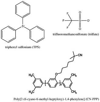
2.2 Instrumentation
For absorption spectra a Perkin-Elmer Lambda-16 spectrometer was employed. Photoluminescence spectra were recorded with a Perkin-Elmer LS-50B fluorescence spectrometer and time-resolved fluorescence measurements were conducted using the time-correlated single-photon counter FL900 of Edinburgh Instruments. All films were spin-coated on quartz substrate and excited at 350 nm. The surface morphology of the pristine polymer and blended polymeric films on quartz substrate was probed with an NT-MDT atomic force microscope (AFM) operated in tapping (semi-contact) mode.2.3 Device fabrication and characterization
Single-layer organic light-emitting diodes (OLEDs) were fabricated on oxygen plasma pre-cleaned transparent indium tin oxide (ITO) coated glass substrates. A 60 nm thick PEDOT:PSS film was spin-coated from a pre-filtered (through a 0.45 μm PVDF filter) aqueous solution onto ITO and annealed in air at 135 °C for at least 15 min. The emitting polymer layer was spin-cast from a 6 mg ml−1 chloroform solution containing the triphenylsulfonium salt in different concentrations (7–30% w/w per polymer mass) resulting in ∼90 nm thick films. All polymer films were annealed at 70 °C for 10 min in air. Finally, a ∼200 nm thick Aluminium cathode was deposited by thermal evaporation through a shadow mask (defined active area of 12.56 mm2) to complete the device structure. Current-voltage characteristics were measured with a Keithley 2400 source-measure unit and luminance and electroluminescence spectral characteristics were recorded with an Ocean Optics spectrophotometer equipped with fiber optics, assuming a Lambertian emission profile (for the luminance measurements). All measurements were carried out in ambient conditions immediately after device fabrication without any encapsulation.3. Results and discussion
3.1 Electrical characteristics of TPS-triflate:CN-PPP based PLEDs
Firstly we investigated the morphology of films both of the polymer alone and blended with triphenylsulfonium triflate salt with atomic force microscopy to check whether the salt addition induces any phase separation (Fig. 2). The pristine CN-PPP film (Fig. 2a) comprises regular round grains homogeneously distributed on the surface with a peak-to-valley height reaching 28.3 nm and an RMS roughness of about 3 nm. Upon addition of 15% TPS-triflate the grains become smaller and the film RMS roughness drops to 1.6 nm, owing probably to the good miscibility of the TPS-triflate in the poly(para-phenylene) matrix (Fig. 2b). This attribute becomes even more pronounced upon addition of 30% TPS-triflate (Fig. 2c), where the film surface becomes smooth and rather featureless, typical of amorphous films, indicating the good dispersion properties of the TPS-triflate in CN-PPP even at high salt concentrations.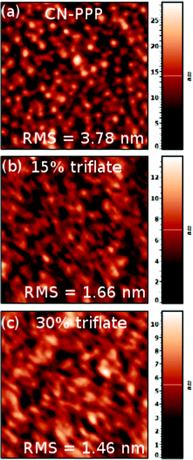 | ||
| Fig. 2 AFM micrographs of (a) pristine CN-PPP film and of films containing (b) 15% TPS-triflate and (c) 30% TPS-triflate. The bars on the right indicate the height differences in nm. | ||
As a next step we fabricated OLEDs with the structure Glass/ITO/PEDOT:PSS/active layer/Al, where the active layer is the poly(para-phenylene) derivative CN-PPP either alone (reference device) or along with 15% and 30% wt per polymer mass of the TPS-triflate. Their current density-voltage (J–V) and luminance-voltage (L–V) characteristics are depicted in Fig. 3. As the concentration of the TPS-triflate increases, the J–V curve shifts to lower bias, meaning that at a constant field (all films have the same thickness) the injected current increases, indicating a more efficient charge injection from the electrodes and enhanced charge transport. More specifically, the current turn-on voltage is a straightforward indication for a beneficial modification of the polymer/anode interface, since the barrier of that interface is smaller and thus a hole current is expected to flow at low voltages. Therefore, the lowering of the current turn-on voltage with increasing TPS-triflate concentration can be attributed to a redistribution of the local field, owing to the anions' movement and subsequent accumulation at the anode side upon application of a bias, leading to a reduced effective barrier for hole injection. On the other hand, the emission of light in OLEDs requires efficient injection from both electrodes as well as enhanced carrier transport. Thus, the luminance turn-on voltage (defined here as the voltage where luminance is approximately 1 cd m−2) can be correlated with the TPS-content of each sample. The electron injection from the cathode is rather problematic in this system, since there is a large barrier of about 1.7 eV (see energy diagram in Fig. 4). Nevertheless, in Fig. 3b (and Fig. S1† in ESI) we observe that the luminance turn-on voltage is substantially lowered from 13.5 V for the reference device to 10 V for the device containing 15% TPS-triflate and to 7 V for the device with 30% TPS-triflate. Similarly, the operating voltage (defined here as the voltage where luminance reaches 100 cd m−2) decreases from 21.5 V for the reference device to 17.5 V and 12 V upon 15% and 30% wt addition of TPS-triflate, respectively. As a result, the efficiencies of the TPS-salt containing OLEDs are higher than that of the reference device, not only in terms of maximum efficiency obtained but also with regard to the efficiencies at a given operation voltage (compare for example the efficiencies at 14 V for each device across the dotted vertical line in the inset of Fig. 3b).
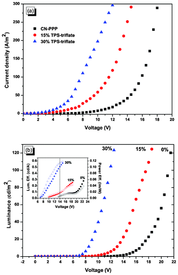 | ||
| Fig. 3 (a) Current density-voltage and (b) luminance-voltage characteristics of OLEDs based on CN-PPP (black squares), 15% TPS-triflate (red circles) and 30% TPS-triflate (blue triangles) in CN-PPP. Inset: luminous (solid symbols) and power (open symbols) efficiencies of the respective devices. | ||
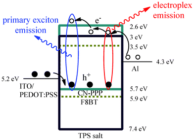 | ||
| Fig. 4 Schematic representation of the energy level alignment in a flat band configuration depicting also the proposed mechanism for light emission. | ||
This obvious concentration dependence of the current- and luminance-voltage characteristics indicates that the TPS-triflate molecules also act as charge transport sites, suggestive of increased bulk conductivity. Such concentration dependence was not observed, for example, when TPS-triflate was added in the green-emitting poly[(9,9-dioctylfluorenyl-2,7-diyl)-co-(1,4-benzo-{2,1′,3}-thiadiazole)] (F8BT) matrix.16 In this case, neither the J–V–L curves nor the turn-on voltage of the devices containing different amounts of TPS-salt varied substantially with the TPS-salt concentration. This can be rationalised by taking into consideration the relative placement of the polymer and the TPS-salt LUMOs. As can be seen from the energy level diagram in Fig. 4, the highest occupied molecular orbital (HOMO) of CN-PPP lies at about 5.7 eV17 and by subtracting the optical energy gap derived from the absorption spectrum (∼3.1 eV) (vide infra), we estimate the position of the CN-PPP lowest unoccupied molecular orbital (LUMO) at about 2.6 eV. On the other hand, the TPS-triflate LUMO is estimated from cyclic voltammetry data to be at about 3 eV.18 Therefore, the LUMO of TPS-triflate lies between the Al Fermi level and CN-PPP LUMO, hence providing available sites for electron hopping and facilitating charge transport in the bulk. This is not the case in the F8BT polymer matrix, whose LUMO level lies lower than the one of TPS-triflate (the energy levels of F8BT are also included in Fig. 4 for comparison), thus enabling F8BT to act as the preferred site for electron transport.
Comparing the system presented here with PLECs, it should be emphasized that here no ionic conductor, such as poly(ethylene oxide), is added in the blend. The devices containing the TPS-salts did not present any significant delay at their turn-on time, which was found to be in the regime of seconds, faster even than the response times reported e.g. for conjugated polyelectrolytes used as thin EILs in PLEDs.19 Besides, we did not need to pre-bias the devices and the lowering of the turn-on voltage was apparent from the first scan. On the other hand, the fact that the luminance turn-on voltage is not close to the energy gap divided by the elementary charge (Eg/e) of the polymer used (i.e. at about 3.1 V) means that no ohmic contacts were formed at both polymer/electrode interfaces, which is consistent with our hypothesis of the TPS-salt being rather static. From all the above we infer that our devices do not behave as the typical polymer light-emitting electrochemical cell (PLEC) in spite of the presence of ions in the active layer. The salts presented here provide the advantage, compared to previously reported inorganic (e.g. FeCl3, LiBr)20,21 or organic salt (i.e. the well-known supporting electrolytes Bu4NPF6, Bu4NBF4, TEAP, etc.)22–24 doped conjugated polymer matrices, that they do not require a thermal and/or electrical treatment step for the activation of the ions.25,26 This deviation from the typical ion-incorporating devices behaviour should be attributed to the intrinsic conductivity of TPS cations, due to their high phenyl ring content, as well as to their homogeneous distribution up to high concentrations in the polymer matrix, which is more easily obtained due to their predominant organic character.
3.2 Photophysical properties – electroplex formation
In order to gain more insight into the photophysics of the devices we recorded the absorption and photoluminescence spectra of the CN-PPP films with and without the TPS-triflate additive (Fig. 5). The absorption spectra are unaffected by TPS-triflate addition, all showing the π–π* peak at 350 nm, whereas increased absorption in the UV part of the spectrum, right below the absorption onset of TPS-triflate at 280 nm, was detected. The absorption spectrum of a bare TPS-triflate film on quartz substrate is also plotted in the same scale in order to rationalize the increase in the UV absorption band upon increased TPS-triflate concentration and to verify that no new species is formed in the ground state, but the spectra of the blends are a simple superposition of each compound's individual spectrum.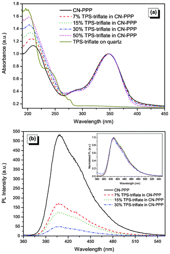 | ||
| Fig. 5 (a) Absorption (normalised to the polymer main peak at 350 nm), (b) PL and normalized PL (inset) spectra of CN-PPP with increasing TPS-triflate concentration. | ||
On the other hand, the photoluminescence measurements reveal that the emission intensity of CN-PPP is strongly attenuated as the % wt of the TPS-triflate increases. The PL intensity of CN-PPP with the 7% wt TPS-triflate (corresponding to 3.8% mol, i.e., 0.038 TPS![[thin space (1/6-em)]](https://www.rsc.org/images/entities/char_2009.gif) :monomer molar ratio) film is decreased by ca. 30%, whereas the one with 30% wt of the salt (corresponding to 16.6% mol, i.e., 0.17 TPS:monomer molar ratio) is attenuated by 70% compared to the pristine polymer spectrum. Note that the excited state (exciton) is delocalised over the conjugation length, which usually includes 3–5 monomer units. The effectiveness of the polymer fluorescence quenching by TPS can be also supported by the linearity of the Stern–Volmer plot of the PL intensity decrease upon increasing the TPS concentration, which is presented in Fig. S2 in ESI.† The origin of the CN-PPP photoluminescence quenching upon salt addition could be better explained by taking into account the relative positions of the LUMOs of the polymer and that of the TPS-triflate. As can be seen from the energy level diagram in Fig. 4, the TPS-triflate LUMO lies 0.4 eV lower than that of the polymer. Therefore, the partial quenching of the photoluminescence could be attributed to photoinduced electron transfer from the polymer LUMO to that of TPS-triflate. Note that the shape of the CN-PPP PL spectra is not at all influenced by the TPS-triflate addition and they resemble closely the primary excitonic emission of the polymer, with the main peak appearing in all cases at 410 nm (see normalised spectra in the inset graph of Fig. 5b). Note, also, that a shoulder appears at about 430 nm, which tends to become more prominent as the concentration of the polymer solution, from which the film is cast, increases (see ESI, Fig. S3†). This is an indication that this shoulder likely corresponds either to an excimer formed upon interaction of a monomer exciton with a neighbouring non-excited monomer at the polymeric chain or, alternatively, it is a vibronic progression of the main emission peak owing to different conformation of the polymer chains. In order to clarify the origin of this spectral feature, we performed time-resolved photoluminescence measurements in CN-PPP films and films containing 15% wt of TPS-triflate in CN-PPP and the results are presented in ESI.† The obtained experimental data do not suggest the formation of an excimer species between excited and ground state polymeric chain segments, since the measured lifetimes are extremely short, whereas excimer emission is generally characterized by slower decay rates. It should be mentioned here that amplified spontaneous emission (ASE) data by Chang et al. showed a similar red shifted emission in CN-PPP, which was attributed to the fact that, upon increasing singlet exciton concentration, the exciton can move to another emitting center and be dissipated with subsequent radiative decay.27
:monomer molar ratio) film is decreased by ca. 30%, whereas the one with 30% wt of the salt (corresponding to 16.6% mol, i.e., 0.17 TPS:monomer molar ratio) is attenuated by 70% compared to the pristine polymer spectrum. Note that the excited state (exciton) is delocalised over the conjugation length, which usually includes 3–5 monomer units. The effectiveness of the polymer fluorescence quenching by TPS can be also supported by the linearity of the Stern–Volmer plot of the PL intensity decrease upon increasing the TPS concentration, which is presented in Fig. S2 in ESI.† The origin of the CN-PPP photoluminescence quenching upon salt addition could be better explained by taking into account the relative positions of the LUMOs of the polymer and that of the TPS-triflate. As can be seen from the energy level diagram in Fig. 4, the TPS-triflate LUMO lies 0.4 eV lower than that of the polymer. Therefore, the partial quenching of the photoluminescence could be attributed to photoinduced electron transfer from the polymer LUMO to that of TPS-triflate. Note that the shape of the CN-PPP PL spectra is not at all influenced by the TPS-triflate addition and they resemble closely the primary excitonic emission of the polymer, with the main peak appearing in all cases at 410 nm (see normalised spectra in the inset graph of Fig. 5b). Note, also, that a shoulder appears at about 430 nm, which tends to become more prominent as the concentration of the polymer solution, from which the film is cast, increases (see ESI, Fig. S3†). This is an indication that this shoulder likely corresponds either to an excimer formed upon interaction of a monomer exciton with a neighbouring non-excited monomer at the polymeric chain or, alternatively, it is a vibronic progression of the main emission peak owing to different conformation of the polymer chains. In order to clarify the origin of this spectral feature, we performed time-resolved photoluminescence measurements in CN-PPP films and films containing 15% wt of TPS-triflate in CN-PPP and the results are presented in ESI.† The obtained experimental data do not suggest the formation of an excimer species between excited and ground state polymeric chain segments, since the measured lifetimes are extremely short, whereas excimer emission is generally characterized by slower decay rates. It should be mentioned here that amplified spontaneous emission (ASE) data by Chang et al. showed a similar red shifted emission in CN-PPP, which was attributed to the fact that, upon increasing singlet exciton concentration, the exciton can move to another emitting center and be dissipated with subsequent radiative decay.27
Electroluminescence data (Fig. 6) were not always in agreement with the photoluminescence data, revealing clearly the different mechanisms governing the two cases.28 Indeed, as can be deduced from the L–V curves (Fig. 3b), the devices with TPS-triflate exhibited (at low voltages) enhanced light output, showing that here, in contrast to photoluminescence, improved charge injection and transport leads to increased charge balance and thus more efficient recombination. Fig. 6a shows the EL spectra of the TPS-triflate:CN-PPP devices and the PL spectrum of CN-PPP, which is also plotted for comparison. The EL spectrum of the reference CN-PPP OLED shows a main peak at 410 nm, similar to PL, but it is broader (FWHM increases from 52 nm in the PL to 84 nm in the EL spectrum of CN-PPP) and the shoulder at 430 nm is much more prominent than in the PL spectrum. Therefore, we have no indication for electromer formation in the plain polymer film, as has been observed for instance in poly(N-vinylcarbazole) films.29 Besides, the EL spectra of the TPS-triflate:CN-PPP devices are considerably different than the spectrum of the reference device. Firstly, the main excitonic peak at 410 nm becomes narrower, resembling closely the PL spectrum of CN-PPP, whereas the absence of the shoulder at 430 nm indicates that TPS-triflate molecules effectively separate polymer chains, disrupting aggregate formation in CN-PPP, which is in accordance with the AFM measurements.
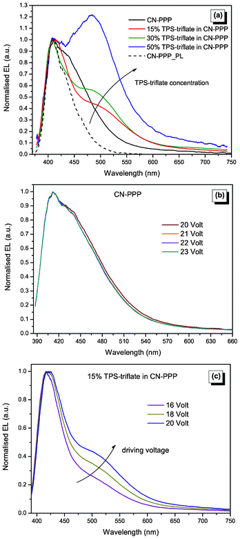 | ||
| Fig. 6 (a) Normalised EL spectra of CN-PPP based OLEDs upon increasing concentration of TPS-triflate. The normalised PL spectrum of CN-PPP is also shown for comparison. (b) Normalised EL spectra of pristine CN-PPP and (c) of 15% TPS-nonaflate in CN-PPP based OLEDs upon increasing the driving voltage. | ||
Furthermore, another interesting feature of these spectra is that a totally new peak is being formed at ca. 483 nm, which becomes dominant at high concentrations. We hypothesize that this red-shifted emission peak comes from a new species, namely a bimolecular charge transfer complex, which may be formed in the excited state between TPS-triflate acceptor molecules and polymeric donor chains, a so-called electroplex. Electroplex emission from bilayer-structured OLEDs as well as from blends has been previously reported and analysed in the literature, for instance between thiophene,30 diamines31 or carbazole moieties and oxadiazoles,32 phenanthrolines,33 siloles,34 quinoxalines,35 terbium complexes36etc. Note that such species differentiate themselves from exciplexes, in that they can be generated solely under electrical excitation.37 The probability for e–h cross recombination at the CN-PPP:TPS-salt interface is directly proportional to the injection and accumulation rate, which increases with the applied field, meaning that this emission should be enhanced as voltage increases.31,33 Indeed, if we compare the normalised EL spectra evolution of CN-PPP (Fig. 6b) and a 15% TPS-triflate:CN-PPP blend based OLED (Fig. 6c), we see that the former EL spectra do not depend on the applied voltage, whereas the spectra of the blend show a clear increase of the electroplex-assigned peak.
To sum up, the mechanism accounting for the emission profiles and its relation to enhanced charge transport in the OLEDs based on TPS-triflate/CN-PPP emissive layers is depicted schematically in Fig. 4. Firstly, upon application of a bias, anions drift to the anode side and a space charge is formed there enhancing hole injection to the emitting layer, as described previously. From the tentative energy diagram, and as far as the polymer/TPS-salt interfaces in the blend are concerned, we deduce that Δ(HOMO) = 1.7 eV and Δ(LUMO) = 0.4 eV. The large HOMO energy difference suggests that injected holes would favourably accumulate at the CN-PPP:TPS-salt interface. At the same time, the TPS salts dispersed inside the polymer matrix can have a double influence over electron transport; electrons injected from the Al cathode to energetically favourable TPS sites can be either transferred to the polymer LUMO, since the barrier for electron transfer is not very large (0.4 eV), or transported via hopping among TPS ions, accumulate there and sequentially stimulate the cross recombination with holes located on the HOMO level of CN-PPP.
Finally, we would like to mention that the TPS-triflate salt can possibly be sensitised by electron transfer from the polymer or the electrode and undergo decomposition via C-S bond cleavage. Although from the data presented in this paper we cannot unambiguously claim that the TPS cleavage is totally avoided, the fact that we observe luminescence and indeed the emission of an electroplex provides a strong indication that such a cleavage is not predominant. In particular, the electroplex emission indicates that the radiative deactivation of the excited state competes with the TPS decomposition via C-S bond cleavage, since in the case of the latter no fluorescence should be observed.38 However, a more detailed study that will involve different sulfonium salts is needed to confirm the above statement. The fact that the energy levels position and/or the antibonding orbital type (e.g. of predominant σ* vs. π* character) of the sulfonium salts can be tuned either by increasing the size of the aryl ring (e.g. replacing phenyl with anthracene)39 or by incorporating suitable substituents in the phenyl rings,18 or even by applying a para-to-meta substitution,40 offers a large variety of possibilities for optimizing the energetic matching with the respective polymer HOMO–LUMO levels and controlling thus at will the photophysical and/or photochemical properties of the blend.
Conclusions
In this work, we showed that triphenylsulfonium triflate can be easily incorporated at high concentrations in the active layer of organic light-emitting diodes and favour the charge injection and transport not only due to its ionic nature but also in view of its favourable alignment with the electrodes and the polymer energy levels. Hence, we demonstrated that the electrical characteristics of blue-emitting OLEDs can be improved by redistributing the field upon anions' accumulation and space charge formation at the anode side and by facilitating electron transport in the bulk, leading to significantly reduced device operating voltage, which is an important feature for energy efficient products. It was also found that the TPS-salt addition influences the emission spectrum by controlling the formation of a lower energy excited state heterocomplex, namely an electroplex. This red-shifted emission is being formed at the interface of negatively charged TPS-salt molecules and positively charged CN-PPP polarons. Such a spectral feature may be beneficial for white light as well as for dimmed lighting applications.The triphenylsulfonium triflate salt presented in this work can act as a model compound for future optimization towards high performance organic light-emitting devices using all-organic sulfonium salts. This is a novel application field for these materials, whose functional properties can be easily tailored through proper selection of both anions and cations. Besides, the exploration of the optoelectronic characteristics of films constituted by triphenylsulfonium salts blended in conjugated polymer matrices can be useful in imaging applications, since these salts are well-known photoacid generators used in the area of photolithographic materials.
References
- J. H. Burroughes, D. D. C. Bradley, A. R. Brown, R. N. Marks, K. Mackay, R. H. Friend, P. L. Burns and A. B. Holmes, Nature, 1990, 347, 539 CrossRef CAS.
- A. P. Kulkarni, C. J. Tonzola, A. Babel and S. A. Jenekhe, Chem. Mater., 2004, 16, 4556 CrossRef CAS.
- Q. B. Pei, G. Yu, C. Zhang, Y. Yang and A. J. Heeger, Science, 1995, 269, 1086 CAS.
- Q. B. Pei, Y. Yang, G. Yu, C. Zhang and A. J. Heeger, J. Am. Chem. Soc., 1996, 118, 3922 CrossRef CAS.
- J. C. deMello, N. Tessler, S. C. Graham and R. H. Friend, Phys. Rev. B: Condens. Matter, 1998, 57, 12951 CrossRef CAS.
- Q. J. Sun, Y. F. Li and Q. B. Pei, J. Disp. Technol., 2007, 3, 211 CrossRef CAS.
- S. Panozzo, M. Armand and O. Stephan, Appl. Phys. Lett., 2002, 80, 679 CrossRef CAS.
- A. Duarte, K. Y. Pu, B. Liu and G. C. Bazan, Chem. Mater., 2011, 23, 501 CrossRef CAS.
- J. V. Crivello, Adv. Polym. Sci., 1984, 62, 1 CrossRef CAS.
- E. Reichmanis, F. M. Houlihan, O. Nalamasu and T. X. Neenan, Chem. Mater., 1991, 3, 394 CrossRef CAS.
- A. M. Douvas, F. Van Roey, M. Goethals, K. G. Papadokostaki, K. Yannakopoulou, D. Niakoula, E. Gogolides and P. Argitis, Chem. Mater., 2006, 18, 4040 CrossRef CAS.
- C. D. Muller, A. Falcou, N. Reckefuss, M. Rojahn, V. Wiederhirn, P. Rudati, H. Frohne, O. Nuyken, H. Becker and K. Meerholz, Nature, 2003, 421, 829 CrossRef.
- M. C. Gather, A. Kohnen, A. Falcou, H. Becker and K. Meerholz, Adv. Funct. Mater., 2007, 17, 191 CrossRef CAS.
- M. Vasilopoulou, D. Georgiadou, G. Pistolis and P. Argitis, Adv. Funct. Mater., 2007, 17, 3477 CrossRef CAS.
- D. G. Georgiadou, M. Vasilopoulou, G. Pistolis, L. Palilis, D. Dimotikali and P. Argitis, Phys. Status Solidi A, 2008, 205, 2526 CrossRef CAS.
- D. G. Georgiadou, L. C. Palilis, M. Vasilopoulou, G. Pistolis, D. Dimotikali and P. Argitis, J. Mater. Chem., 2011, 21, 9296 RSC.
- Y. Yang, Q. Pei and A. J. Heeger, J. Appl. Phys., 1996, 79, 934 CrossRef CAS.
- K. H. Vase, A. H. Holm, K. Norrman, S. U. Pedersen and K. Daasbjerg, Langmuir, 2008, 24, 182 CrossRef CAS.
- C. Hoven, R. Yang, A. Garcia, A. J. Heeger, T. Q. Nguyen and G. C. Bazan, J. Am. Chem. Soc., 2007, 129, 10976 CrossRef CAS.
- D. B. Romero, M. Schaer, L. Zuppiroli, B. Cesar and B. Francois, Appl. Phys. Lett., 1995, 67, 1659 CrossRef CAS.
- W. Zhao and J. M. White, Appl. Phys. Lett., 2005, 87(1), 103503 CrossRef.
- C. C. Yap, M. Yahaya and M. M. Salleh, Curr. Appl. Phys., 2009, 9, 722 CrossRef.
- Y. Sakuratani, M. Asai, M. Tokita and S. Miyata, Synth. Met., 2001, 123, 207 CrossRef CAS.
- E. Itoh, T. Yamashita and K. Miyairi, J. Appl. Phys., 2002, 92, 5971 CrossRef CAS.
- S. S. Oh, J. H. Park, S. W. Kim and B. C. Park, J. Appl. Phys., 2007, 102(1), 74503 CrossRef.
- Y. Shao, G. C. Bazan and A. J. Heeger, Adv. Mater., 2007, 19, 365 CrossRef CAS.
- J. Chang, J. Han, J. An, C. Im, Y. J. Yu and J. I. Jin, J. Korean Phys. Soc., 2007, 51, 1993 CrossRef CAS.
- J. Kalinowski, G. Giro, M. Cocchi, V. Fattori and P. Di Marco, Appl. Phys. Lett., 2000, 76, 2352 CrossRef CAS.
- T. L. Ye, J. S. Chen and D. G. Ma, Phys. Chem. Chem. Phys., 2010, 12, 15410 RSC.
- M. Berggren, G. Gustafsson, O. Inganas, M. R. Andersson, T. Hjertberg and O. Wennerstrom, J. Appl. Phys., 1994, 76, 7530 CrossRef CAS.
- J. Kalinowski, M. Cocchi, P. Di Marco, W. Stampor, G. Giro and V. Fattori, J. Phys. D: Appl. Phys., 2000, 33, 2379 CrossRef CAS.
- X. Z. Jiang, R. A. Register, K. A. Killeen, M. E. Thompson, F. Pschenitzka, T. R. Hebner and J. C. Sturm, J. Appl. Phys., 2002, 91, 6717 CrossRef CAS.
- Y. M. Wang, F. Teng, Z. Xu, Y. B. Hou, S. Y. Yang, L. Qian, T. Zhang and D. A. Liu, Appl. Surf. Sci., 2004, 236, 251 CrossRef CAS.
- L. C. Palilis, A. J. Makinen, M. Uchida and Z. H. Kafafi, Appl. Phys. Lett., 2003, 82, 2209 CrossRef CAS.
- X. J. Xu, G. Yu, S. Y. Chen, C. A. Di and Y. Q. Liu, J. Mater. Chem., 2008, 18, 299 RSC.
- H. Xin, M. Guang, F. Y. Li, Z. Q. Bian, C. H. Huang, K. Ibrahim and F. Q. Liu, Phys. Chem. Chem. Phys., 2002, 4, 5895 RSC.
- J. Kalinowski, Materials Science-Poland, 2009, 27, 735 CAS.
- M. Yasuike, K. Koseki, T. Yamaoka, K. Ichimura, M. Sakuragi and O. Ohno, Inorg. Chim. Acta, 1991, 183, 9 CrossRef CAS.
- F. D. Saeva, D. T. Breslin and P. A. Martic, J. Am. Chem. Soc., 1989, 111, 1328 CrossRef CAS.
- R. J. Xia, J. P. Malval, M. Jin, A. Spangenberg, D. C. Wan, H. T. Pu, T. Vergote, F. Morlet-Savary, H. Chaumeil, P. Baldeck, O. Poizat and O. Soppera, Chem. Mater., 2012, 24, 237 CrossRef CAS.
Footnote |
| † Electronic Supplementary Information (ESI) available: Enlarged detail of Fig. 3b, Stern–Volmer plots of the quenching process, photoluminescence spectra of CN-PPP films cast from different concentration solutions and time-resolved photoluminescence spectroscopy results are provided as supplementary information. See DOI: 10.1039/c2ra21709k |
| This journal is © The Royal Society of Chemistry 2012 |