DOI:
10.1039/C2RA21662K
(Paper)
RSC Adv., 2012,
2, 9606-9613
Controlled and stepwise generation of Cu2O, Cu2O@Cu and Cu nanoparticles inside the transparent alumina films and their catalytic activity†
Received
28th February 2012
, Accepted 12th August 2012
First published on 15th August 2012
Abstract
A stepwise generation of Cu2O, Cu2O@Cu core-shell and Cu nanoparticles (NPs) inside the alumina films has been accomplished. First, CuO–Al2O3 films were prepared on glass substrates by dip-coating method using alumina sol derived from partially acetylacetonate (acac) chelated aluminium-tri-sec-butoxide doped with copper(II) chloride, followed by heat-treatment at 450 °C in air. Heat-treatment of CuO–Al2O3 films at 450–500 °C in reducing atmosphere resulted in the formation of stable Cu2O NPs which can be subsequently converted to Cu2O@Cu core-shell NPs with tunable Cu-shell thickness, and followed by pure Cu NPs by further heat-treatment at 550–700 °C. UV–visible, transmission electron microscopy (TEM) and grazing incidence X-ray diffraction (GIXRD) studies of the films in different stages confirmed the generation of Cu2O, Cu2O@Cu core-shell and Cu NPs. It has been understood that the chemical structure and property of matrix alumina facilitated the stabilization of Cu2O NPs inside the films. As a result, the formation of Cu2O@Cu NPs can be achieved easily by controlled heat-treatment in reducing atmosphere. The catalytic properties of Cu2O, Cu2O@Cu and Cu NPs incorporated alumina films were studied by monitoring the degradation of an azo dye congo-red. All films showed very good catalytic activities; among these Cu2O NPs doped films showed excellent stability, reusability and high rate constant values.
Introduction
As a p-type semiconductor (direct band gap 2.17 eV) with unique optical and electrical properties,1,2 cuprous oxide (Cu2O) is a promising material with potential applications in solar energy conversion,3 magnetic storage devices,4 biosensors,5 catalysis,6 antibacterial activity7 and gas sensors.8 Cu2O micro and nanostructures with various shapes such as cubic9 and hollow cubic,10 hollow spherical,11 octahedral,12 triangular platelike13 and pyramidal14 as well as core-shell nanocomposites15–17 following different synthetic protocols such as electrodeposition,18 arc discharge,19 sonochemical20 and polyol reduction methods21 have been synthesized. A few reports are available in the literature regarding the synthesis of Cu2O@Cu core-shell NPs in solution.15–17 It is noteworthy that generation of a Cu2O shell on Cu core (Cu@Cu2O) is quite trivial due to the easy generation of an oxide shell when Cu metal NPs are exposed to the atmosphere. However, the reverse type of core-shell, i.e. Cu2O@Cu composite particles in the nano regime, is rare in the literature. Synthesis of few micron sized Cu2O@Cu particles was reported, where the outer surface of Cu2O had been partly converted to Cu after addition of strong reducing agent like hydrazine.22,23 Another report showed the conversion of hydrothermally synthesized Cu2O to Cu2O@Cu particles having size of 5–6 microns by increasing the aging time of the reaction mixture.24 Besides these solution based synthetic protocols, formation of Cu2O and Cu2O@Cu NPs in a dielectric film matrix is not reported in the literature. The semiconductor core-metal shell composite NPs are of increasing scientific and technological interest due to an expanding and wide range of applications.25,26 The optical properties of the nano-shell are often influenced by the properties of the core material.25 Efficiency of photocatalytic reactions can be maximized by promoting inter-facial charge transfer processes in these composite systems.26b Tuning the sensing properties and tailoring the photoelectrochemical properties of the core materials remain a major challenge of designing semiconductor core-metallic shell composite systems. It can be noted that, in general, bulk cupric oxide (CuO) transforms to metallic Cu when heat-treated in reducing atmosphere, without the formation of stable intermediate phases such as Cu2O.27 Further, in SiO2 matrix, Cu2O NPs are not found to be formed as a stable intermediate phase,28 as Cu2+ reduces mainly to Cu0. We found that the Cu+ state can be stabilized inside the alumina film matrix and it is possible to generate subsequently a core-shell structure comprising Cu2O as core and Cu as shell (Cu2O@Cu) from the initially formed Cu2O NPs by controlled heat-treatment in reducing atmosphere. Finally this core-shell structure can be transformed to pure Cu NPs inside the alumina film. In this paper we report an easy and step-by-step synthesis of Cu2O (semiconductor), Cu2O@Cu (semiconductor core and metal shell) with tunable Cu-shell thickness and Cu (metal) NPs inside Al2O3 film matrix starting from a sol–gel derived Cu2+ doped Al2O3 film. As these NPs are embedded in the transparent alumina film matrix, use of the films as catalyst could be advantageous over bare NPs, thus ensuring all the unique characteristics of catalyst film.29 Keeping in view the cost-effectiveness compared to the use of expensive NPs for catalytic process,30 involvement of complicated photocatalytic,31 sonophotocatalytic31 and γ-ray irradiation processes,32 the catalytic behaviour of Cu2O, Cu2O@Cu and Cu NPs embedded alumina films towards the decomposition of congo-red dye has been studied and reported as one of the applications.
Experimental
Materials
All chemicals were used as received. Aluminum-tri-sec-butoxide Al[OCH(CH3)C2H5]3 (ASB) and congo-red (C32H22N6Na2O6S2) were supplied by Sigma-Aldrich; while acetylacetone (acac), 1-propanol and 2-butanol were obtained from s.d. fine-chem limited. CuCl2·2H2O was obtained from Qualigens fine chemicals. Mili-Q (Millipore) water (18 MΩ) was used throughout the study. Compressed gas mixture 10% hydrogen, balance argon was obtained from BOC India Ltd.
Preparation of ASB Stock Solution and Cu doped ASB sol
The ASB stock solution was prepared following the procedure reported in our previous paper with modifications.33 First, a partially acetylacetonato complexed ASB stock solution was prepared in the following way: the required amount of ASB was quickly transferred to a 1-propanol–2-butanol (3![[thin space (1/6-em)]](https://www.rsc.org/images/entities/char_2009.gif) :2 w/w ratio) solution of acac with stirring at room temperature and the resulting mixture was stirred for another 1 h in a sealed container. The molar ratio of acac/ASB used was 0.4, and this acac modified sol is designated as ASB0.4acac. The concentration of ASB in this partially acetylacetonato complexed ASB stock solution was about 35 wt%. The required amount of CuCl2·2H2O dissolved in water and 1-propanol mixture was mixed with the sol with stirring. Subsequently two drops (∼0.0012 g) of concentrated HNO3 was added in the sol and the stirring was continued for another 30 min. The Cu concentration was maintained at 10 mol% with respect to the equivalent amount of AlO1.5 present in the sol. In the final sol, the required amount of 1-propanol was added to adjust the AlO1.5 concentration to 4.5 equivalent wt%.
:2 w/w ratio) solution of acac with stirring at room temperature and the resulting mixture was stirred for another 1 h in a sealed container. The molar ratio of acac/ASB used was 0.4, and this acac modified sol is designated as ASB0.4acac. The concentration of ASB in this partially acetylacetonato complexed ASB stock solution was about 35 wt%. The required amount of CuCl2·2H2O dissolved in water and 1-propanol mixture was mixed with the sol with stirring. Subsequently two drops (∼0.0012 g) of concentrated HNO3 was added in the sol and the stirring was continued for another 30 min. The Cu concentration was maintained at 10 mol% with respect to the equivalent amount of AlO1.5 present in the sol. In the final sol, the required amount of 1-propanol was added to adjust the AlO1.5 concentration to 4.5 equivalent wt%.
Preparation of Cu2O, Cu2O@Cu and Cu NPs doped alumina films
The above-mentioned sol was used for film deposition on glass substrates. Prior to film deposition, the soda-lime and silica glass slides were thoroughly cleaned as usual. The films were prepared from Cu doped sol by a single dipping technique with a withdrawal velocity of 20 cm min−1. The as prepared films were dried at 60 °C for 30 min. After that the films were heat-treated at 450 °C (ramp at 2 °C min−1) in air with a holding time of 1 h. For the preparation of Cu2O NPs embedded film, these films were heat-treated at 450 °C in 10% H2 and 90% Ar (will be designated as H2–Ar hereafter) atmosphere for 30 min with a gas flow rate of 45 bubbles per min. The number of gas bubbles was counted at the gas outlet using a water filled Dreschel bottle. Further heat-treatment of this film at 460, 480 and 500 °C with 30 min holding time in each step in a cumulative heating procedure in H2–Ar with the same gas flow rate resulted in the formation of Cu2O@Cu NPs inside the film. Cu NPs doped films were obtained by heat-treating these Cu2O@Cu NPs doped films at 550–700 °C in H2–Ar with a holding time of 1 h.
Characterization techniques
The UV–vis spectra of coatings deposited on glass substrates were obtained using a Cary 50 scan spectrophotometer. Infrared absorption spectra of the sols (by placing the liquid sample between two KBr windows) and films (deposited on Si-wafers) were recorded by FTIR spectrometer (Nicolet 380) with 200 scans for each sample. Thickness and refractive index measurement of the films deposited on Si wafer was done using a J. A. Woollam Co. M 2000 spectroscopic ellipsometer. GIXRD patterns of the films were recorded by using Rigaku SmartLab operating at 9 kW (200 mA and 45 kV) using Cu-Kα (λ = 1.5406 Å) radiation. 0.3° grazing incidence angle was used for all the measurements. Field emission scanning electron microscopic (FESEM) images were taken using ZEISS SUPRA 35VP. TEM measurements were carried out with a Tecnai G2 30ST (FEI) operating at 300 kV. For the TEM study scratched off film samples were placed on the carbon coated Mo grids followed by a drop of methanol and dried at room temperature. The energy dispersive X-ray scattering (EDS) analyses of the Cu doped films were obtained by the EDS facilities attached with TEM.
Catalytic activities
Cu2O, Cu2O@Cu and Cu NPs doped alumina films were used to study the catalytic activities for the decomposition of congo-red dye. The catalytic studies were performed using one piece of both side coated doped alumina film deposited on soda lime glass substrate of approximate dimensions 1.25 cm × 0.8 cm × 260 nm (film thickness) and placing them in the reaction mixture of 2.95 ml of 0.5 × 10⁻⁴ M congo-red dye solution and 0.05 ml of 0.15 M NaBH4 solution in the cuvette cell in such a way that the surfaces of the catalysts should not touch or overlap each other. The reaction was studied at 25 °C with constant stirring to ensure the homogeneous mixing of the reaction mixture. The evolution of absorption spectra due to the decomposition of congo-red dye was recorded using a Cary 50 scan UV–visible spectrometer attached with a Peltier temperature controller in kinetic mode operation. Spectra were also recorded in absence of catalysts. To test the reusability of the films, the used films were washed with distilled water and then dried at 60 °C for 10 min. These films were then ready for next time use. Reaction conditions were maintained similarly in all cases using Cu2O, Cu2O@Cu and Cu NPs embedded alumina films.
Results and discussion
Stepwise generation of Cu2O, Cu2O@Cu and Cu NPs inside the alumina films
10 mol% CuCl2 doped alumina sol was used to prepare coatings on soda-lime and silica glass substrates. As prepared and 60 °C dried films were transparent and faintly greenish in colour. Films were first heat-treated in air at 450 °C to remove the organics. At this stage Cu remains as Cu2+ (CuO) in the alumina film. These air-annealed films (CuO/Al2O3) were, when heat-treated at 450 °C in H2–Ar, transformed to yellow-greenish, and Cu2O NPs are supposed to be formed (designated as Film A). Heat-treatment of this film at 460, 480 and 500 °C in H2–Ar led to the formation of reddish-yellow films. These alumina films are expected to contain Cu as well as Cu2O species and are designated as Films B (460 °C), C (480 °C) and D (500 °C). Further heat-treatment of the film at 550–700 °C in H2–Ar for 1 h yielded pure Cu NPs inside the alumina film (550 °C and 700 °C heat-treated films have been designated as Films E and F). All the heat-treated films were visually transparent and crack free.
UV–visible studies
Formation of the Cu2O, Cu2O@Cu and Cu NPs inside the alumina film was first indicated by the UV–visible spectrometry. UV–visible spectra of the films along with the air-annealed CuO/Al2O3 film are shown in Fig. 1a. The air-annealed film (CuO/Al2O3) shows a very weak and broad peak centred at ∼700 nm (Fig. 1a, curve i, enlarged portion shown in the inset as ‘A’) due to the d–d transition of Cu2+ (3d9 system). The observed d–d transitions are in the range expected for Cu2+ species in an axially distorted octahedral (due to Jahn–Teller effect) environment of O-containing ligands.28a Film A (annealed at 450 °C in H2–Ar) shows weak absorption peak at ∼350 nm which is attributed to the band-to-band transition,15 indicating the presence of Cu2O (Fig. 1a, curve ii). Besides this, two intrinsic band-gap absorptions of Cu2O can be observed near 450 nm and 585 nm (weak).34 Films C and D (annealed at 480 and 500 °C in H2–Ar) show almost similar absorption behaviour as that of Film A, but a weak absorption peak can be observed near 575 nm (Fig. 1a, curves iii and iv). This gives an indication that some Cu NPs have been formed at these stages because the 575 nm band can be assigned as the surface plasmon resonance (SPR) band of Cu NPs. Film F shows an intense peak at 575 nm due to Cu-SPR indicating the presence of Cu NPs in the film (Fig. 1a, curve v). In this case absence of lower wavelength peaks (as observed in cases of Films A, C and D) indicates that all Cu2O NPs have been converted to Cu NPs.
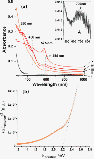 |
| | Fig. 1 (a) Optical absorption spectra of CuCl2 doped alumina films after heat-treatment at different temperatures in cumulative heating procedures: (i) 450 °C in air, (ii) 450 °C in H2–Ar/30 min (Film A), (iii) 480 °C in H2–Ar/30 min (Film C), (iv) 500 °C in H2–Ar/30 min (Film D) and (v) 700 °C in H2–Ar/1 h (Film F). A magnified view of graph ‘i’ has been shown in inset (marked by A) indicating the presence of peak originated from Cu2+. (b) Band gap evaluation from the plot of (αEphoton)2vs. Ephoton for Cu2O NPs embedded in alumina film. | |
Fig. 1b shows the absorption band-gap (Eg) values of the Cu2O NPs embedded alumina film calculated from the absorption curve of Film A (Fig. 1a, curve ii). Band gap energy was estimated using the following equation for semiconductor16
The term hν represents the photon energy, α is the absorption coefficient, α0 is a constant and n has a value of either 2 for a direct transition or ½ for an indirect transition. The optical band-gap is the extrapolated value (the straight line to the X-axis of Fig. 1b) of Ephoton at α = 0 from the plot of (αEphoton)2vs. Ephoton, and gives the absorption edge energy corresponding to Eg = 2.19 eV. The evaluated band gap is little higher than the direct band gap value of bulk Cu2O (2.0–2.17 eV).
FTIR spectrum of ASB0.4acac shows peaks at ∼1597 (νC–C + νC–O) and 1533 cm−1 (νC–O + νC–C) corresponding to the chelated acac groups attached to Al (Fig. 2).35 After doping of CuCl2 into ASB0.4acac, the C–C + C–O combined peak is slightly shifted to lower wavelength. This shifting, evident from both the sol (Fig. 2a) and the film (Fig. 2b), indicates the possibility of formation of Cu–acac linkage to some extent. FTIR spectra of ASB0.4acac as well as CuCl2 doped sol and film confirm the absence of any peak in the 1700 cm−1 region due to free acetylacetone. It indicates that ring opening of acac chelates has not occurred due to the addition of catalytic amount of HNO3 during CuCl2 doping. The spectra of the sol also show the presence of an H–O–H bending vibration at 1645 cm−1 which is due to the water introduced to dissolve CuCl2 and also from HNO3. FTIR spectra of the 450 °C heat-treated undoped alumina and the Film A (Cu2O/Al2O3) (Fig. 2c) show complete absence of organic peaks and the signature of γ-Al2O3.29a,35a In the case of Film A, the peak at 617 cm−1 (see the magnified region in Fig. 2c) corresponds to the vibrational mode of Cu–O in Cu2O phase.36
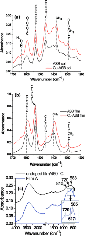 |
| | Fig. 2 FTIR spectra of (a) ASB0.4acac and Cu doped ASB0.4acac sols diluted with 1-propanol; (b) corresponding coatings derived from these sols dried at room temperature. In both cases, similar mol% of AlO1.5 content was maintained. (c) FTIR spectra of undoped alumina film heat-treated at 450 °C in air (1 h) and Film A revealing the formation of γ-Al2O3 and presence of Cu2O in γ-Al2O3, respectively. The Y-axis has been shifted for clarity reason. | |
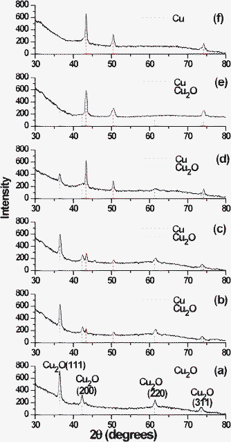 |
| | Fig. 3 GIXRD patterns of Cu doped alumina films after heat-treatment at different temperatures in H2–Ar atmosphere in cumulative heating procedures (a) 450 °C/30 min (Film A); (b) 460 °C/30 min (Film B); (c) 480 °C/30 min (Film C), (d) 500 °C/30 min (Film D), (e) 550 °C/1 h (Film E) and (f) 700 °C/1 h (Film F). Bragg reflection positions of Cu (JCPDS no. 00-004-0836) and Cu2O (JCPDS no. 00-005-0667) with relative intensities are shown as vertical red (Cu) and blue (Cu2O) dash lines, respectively. | |
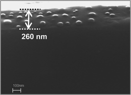 |
| | Fig. 4 FESEM cross-sectional image of the Cu2O NPs embedded alumina film (Film A) showing the presence of NPs along the cross-section. The double-headed arrow represents the film thickness. | |
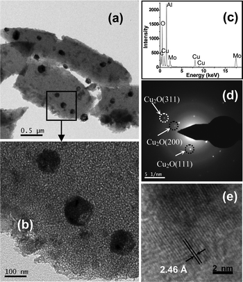 |
| | Fig. 5 (a and b) TEM images of the Cu2O doped alumina film (Film A) with different magnifications; (c) EDS spectrum showing the presence of different elements in the film, Mo is from the Mo grid used for TEM study; (d) SAED pattern obtained from (a); (e) high resolution TEM image of a portion of one Cu2O NP. | |
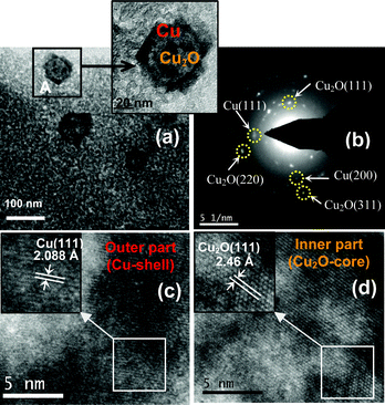 |
| | Fig. 6 (a) TEM images showing the existence of Cu2O@Cu NPs in the alumina film; magnified image of one NP (marked as A) has been shown in the inset indicating the core (Cu2O) and shell (Cu); (b) SAED pattern taken from the NP (shown in the inset of ‘a’, marked as A) confirms the co-existence of Cu and Cu2O in a single NP; (c) HRTEM image of the outer darker portion of the NP shows the lattice fringes corresponding to Cu (a magnified portion has been shown in the inset); (d) HRTEM image taken from the inner lighter portion of the NP showing lattice fringes corresponding to Cu2O NPs (inset shows a magnified portion). | |
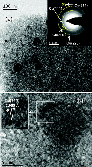 |
| | Fig. 7 (a) TEM image of Cu NPs embedded alumina film (Film F); SAED pattern with labeling of different crystalline planes has been shown in the inset and (b) HRTEM image of one small Cu NP (inset shows a magnified view) showing lattice fringes corresponding to the Cu(111) plane. | |
The UV–visible study at the first instance gave an indication of the formation of Cu2O NPs in the alumina matrix, then the co-existence of Cu and Cu2O and finally its transformation to Cu NPs. The GIXRD study strongly supports the UV–visible study. Firstly GIXRD confirms the formation of Cu2O NPs and subsequently the Cu2O/Cu NPs after controlled reduction of initially formed Cu2O NPs. The ratio of Cu2O/Cu can be tuned by controlling the heat-treatment conditions. At the last stage of reduction the film showed only the diffraction peaks corresponding to Cu. The TEM studies also confirmed the formation of Cu2O@Cu NPs in case of Film D. All these results suggests that the Film B and C have also Cu2O@Cu type structure with expected less shell (Cu) thickness because GIXRD patterns of these films show Cu peaks with relatively low intensity (Fig. 3b and c). Hence the outer surface of the Cu2O NPs (formed in Film A) can be reduced to Cu in a controlled way to obtain Cu2O@Cu core-shell NPs with the variation of core/shell dimensions.
It is noteworthy here that the alumina matrix plays an important role in the formation of Cu2O NPs. After heat-treatment of Cu salt doped alumina film at 450 °C in air, Cu remains as Cu2+ which can be evident from the UV–visible study. When this film is annealed in H2–Ar at 450 °C, Cu2+ partially reduces to the intermediate Cu+. It can be expected that during the heat-treatment of alumina films, very small cubic γ-Al2O3 crystallites would be formed (supported by FTIR studies; see inset of Fig. 2c). As Cu2O has also cubic structure, the embedding cubic γ-Al2O3 host can facilitate the generation of Cu2O and its stabilization. Further, the oxidizing character of γ-Al2O338 can also help to stabilize the intermediate oxidation state of Cu i.e. Cu+. We observed that in other dielectric film matrices such as SiO2, the Cu+ phase can not be stabilized.39 So it can be concluded that the γ-Al2O3 matrix directs the stabilization of the cubic Cu2O (Cu+ state) inside it. Further, controlled thermal treatment in reducing atmosphere causes the reduction of the outer portion of Cu2O into Cu NP, forming a core-shell type structure. Reduction at higher temperature (550–700 °C) converts all the Cu2O to Cu NPs inside the alumina matrix.
Congo-red degradation catalyzed by the films
Cu based catalysts, both metallic and oxides, have been widely used as powerful heterogeneous catalysts.6,40 The Cu-embedded alumina films synthesized in this work can be useful as catalysts because the matrix alumina film is porous in nature.41 From TEM studies (Fig. 5–7 and S3a; ESI†) the porous structure of the embedding alumina matrix can be observed. This was further confirmed from the ellipsometric measurements. Refractive indexes (RI) of the undoped film matrix (at 633 nm) were found to be in the range of 1.505–1.502 after heat-treatment at 450–700 °C under similar experimental conditions as those of Cu incorporated films. The experimentally observed RI values of these heat-treated films are found to be less compared to the dense (1.65) γ-Al2O342 indicating presence of about 20% porosity.43 So these Cu embedded porous alumina films could be useful as catalysts because the porous structure of the alumina films will cause easy accessibility of the solution through the pores, thereby facilitating the catalytic process. As an initial experiment we employed the Cu2O, Cu2O@Cu and Cu NPs embedded alumina films to catalyse the degradation reaction of azo dyes. Azo dyes contribute almost 70% of all used dyes and their degradation is difficult due to their complex structure and synthetic nature. As a representative, congo-red dye, which is considered as a primary toxic pollutant in water resources and having two –N![[double bond, length as m-dash]](https://www.rsc.org/images/entities/char_e001.gif) N– groups, was chosen. The spectrum of congo-red in distilled water exhibits the maximum absorption band centred at 498 nm (Fig. 8a) which could be assigned to the conjugated system formed by the –NN– bonds of congo-red. The red colour of congo-red is due to this maximum absorption band. When an aqueous solution of NaBH4 is added to congo-red solution, no colour change occurs indicating that the degradation of congo-red proceeds very slowly in the presence of NaBH4. The degradation reaction does not proceed also in the presence of undoped alumina film (see inset of Fig. 8a). However, in presence of Cu2O (Film A), Cu2O@Cu (Film D was taken as representative) and Cu NPs embedded films (Film F was taken as representative) the absorption band at 498 nm is found to be decreased and disappeared, which can be ascribed to the breakage of –NN– bonds. Compared to congo-red, its degradation products become inclined to biodegradation and mineralization, largely reducing the harm to the environment.44 UV–visible spectral evolution of the degradation of congo-red dye by Cu2O film (Film A) is shown in Fig. 8a. It can be noted here that the reaction proceeds through a clear isosbestic point at 306 nm indicating that this degradation reaction is proceeding smoothly. The catalytic mechanism involves efficient NP mediated electron transfer from borohydride ions to azo bonds.30 The depletion of 498 nm peak has been used to study the rate of such catalysed reaction. Since the concentration of NaBH4 was taken in excess the reaction was assumed to be of pseudo first order and the rate constant of the reaction was calculated by plotting lnA498vs. time (Fig. 8b). The rate constant value has been determined from the slope of the straight line and found to be 0.567 min−1. After the degradation reaction is over, the film catalysts are simply taken out from the reaction mixture, washed with water and dried at 60 °C for 10 min and they were used next time. Five consecutive cycles were performed to check the reusability of the film catalyst using the same film and only a minute decrease of reaction rate was observed after 5 such cycles. The rate constant values of the degradation reaction catalysed by Cu2O NPs embedded alumina film with respect to the number of cycles are shown in Fig. 8c. It can be seen from Fig. 8c that the film catalyst remains fairly active at least up to 5 cycles of reactions. GIXRD of this film, taken before and after 5 cycles of catalytic reaction, shows no deterioration of Cu2O NPs inside the film (see Fig. S4; ESI†). This reveals that, under the present experimental condition, no degradation or reduction of Cu2O occurred in presence of NaBH4. The rate of degradation of congo-red in five consecutive cycles was found to be lower in cases of Cu2O@Cu and Cu NPs embedded films. Fig. 9 shows the rate constants for the five consecutive cycles catalysed by Cu2O, Cu2O@Cu and Cu NPs embedded alumina films. The above systematic catalytic experiments suggest that the catalytic efficiency of Cu2O NPs is superior than Cu2O@Cu and Cu NPs. Thus the Cu2O NPs embedded alumina film could find important applications in the treatment of waste water, because it has the advantages of being easy to handle, easily separable from the reaction mixture, reusable for several cycles and having non-aggregation of NPs (which causes deterioration of catalytic activity). Moreover, the synthesis process of this film is easy and scalable and would be a cost-effective substitute for the noble metals and other complex processes.30–32 So these film catalysts can be useful as highly efficient reusable catalysts for toxic dye degradation.
N– groups, was chosen. The spectrum of congo-red in distilled water exhibits the maximum absorption band centred at 498 nm (Fig. 8a) which could be assigned to the conjugated system formed by the –NN– bonds of congo-red. The red colour of congo-red is due to this maximum absorption band. When an aqueous solution of NaBH4 is added to congo-red solution, no colour change occurs indicating that the degradation of congo-red proceeds very slowly in the presence of NaBH4. The degradation reaction does not proceed also in the presence of undoped alumina film (see inset of Fig. 8a). However, in presence of Cu2O (Film A), Cu2O@Cu (Film D was taken as representative) and Cu NPs embedded films (Film F was taken as representative) the absorption band at 498 nm is found to be decreased and disappeared, which can be ascribed to the breakage of –NN– bonds. Compared to congo-red, its degradation products become inclined to biodegradation and mineralization, largely reducing the harm to the environment.44 UV–visible spectral evolution of the degradation of congo-red dye by Cu2O film (Film A) is shown in Fig. 8a. It can be noted here that the reaction proceeds through a clear isosbestic point at 306 nm indicating that this degradation reaction is proceeding smoothly. The catalytic mechanism involves efficient NP mediated electron transfer from borohydride ions to azo bonds.30 The depletion of 498 nm peak has been used to study the rate of such catalysed reaction. Since the concentration of NaBH4 was taken in excess the reaction was assumed to be of pseudo first order and the rate constant of the reaction was calculated by plotting lnA498vs. time (Fig. 8b). The rate constant value has been determined from the slope of the straight line and found to be 0.567 min−1. After the degradation reaction is over, the film catalysts are simply taken out from the reaction mixture, washed with water and dried at 60 °C for 10 min and they were used next time. Five consecutive cycles were performed to check the reusability of the film catalyst using the same film and only a minute decrease of reaction rate was observed after 5 such cycles. The rate constant values of the degradation reaction catalysed by Cu2O NPs embedded alumina film with respect to the number of cycles are shown in Fig. 8c. It can be seen from Fig. 8c that the film catalyst remains fairly active at least up to 5 cycles of reactions. GIXRD of this film, taken before and after 5 cycles of catalytic reaction, shows no deterioration of Cu2O NPs inside the film (see Fig. S4; ESI†). This reveals that, under the present experimental condition, no degradation or reduction of Cu2O occurred in presence of NaBH4. The rate of degradation of congo-red in five consecutive cycles was found to be lower in cases of Cu2O@Cu and Cu NPs embedded films. Fig. 9 shows the rate constants for the five consecutive cycles catalysed by Cu2O, Cu2O@Cu and Cu NPs embedded alumina films. The above systematic catalytic experiments suggest that the catalytic efficiency of Cu2O NPs is superior than Cu2O@Cu and Cu NPs. Thus the Cu2O NPs embedded alumina film could find important applications in the treatment of waste water, because it has the advantages of being easy to handle, easily separable from the reaction mixture, reusable for several cycles and having non-aggregation of NPs (which causes deterioration of catalytic activity). Moreover, the synthesis process of this film is easy and scalable and would be a cost-effective substitute for the noble metals and other complex processes.30–32 So these film catalysts can be useful as highly efficient reusable catalysts for toxic dye degradation.
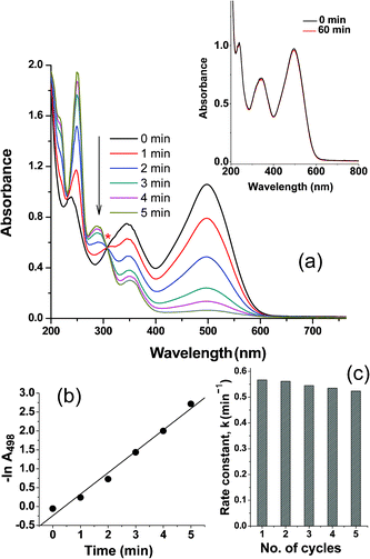 |
| | Fig. 8 (a) Successive UV-visible absorption spectra of the degradation of congo-red in the presence of Cu2O embedded alumina film (Film A) at 25 °C, isosbestic point is shown with asterisk. Similar reaction in the presence of undoped alumina film has been shown in the inset; (b) pseudo first order plot of −lnA (absorbance intensity at 498 nm) vs. time for the above reaction; (c) rate constant values (k) of the catalytic reduction reaction in five consecutive cycles using the same catalyst. | |
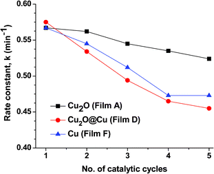 |
| | Fig. 9 Rate constant values of the congo-red degradation reaction in five consecutive cycles using Cu2O (Film A), Cu2O@Cu (Film D) and Cu NPs (Film F) embedded alumina films. | |
Conclusions
In summary, we have developed a simple and effective approach for the preparation of Cu2O NPs in an alumina matrix film. From structural analysis, it can be concluded that the Cu2O phase is highly stabilized in alumina film matrix. After the formation of Cu2O NPs in alumina, controlled reduction by slight modulation of the heat-treatment temperature allows the outer surface of Cu2O to be transformed to Cu to generate Cu2O@Cu NPs with tunable core/shell structure. Optical, GIXRD and electron microscopic studies unequivocally confirm the formation of Cu2O as core and Cu as shell. Further reduction transforms Cu2O@Cu NPs to Cu NPs. Therefore, following this simple and inexpensive approach, copper based NPs with different oxidation states and geometry can be synthesized inside the transparent alumina film matrix in a systematic stepwise manner. It is noteworthy that all these products synthesized in a cumulative way, especially the Cu2O@Cu NPs incorporated alumina film, deserve attention for different important technological applications e.g. tuning of linear and non-linear optical properties, optical limiting applications to control high intensity laser lights, solar energy conversion, tailoring the photoelectrochemical, sensing and catalytic properties.25,26 As one of the representative applications, we found that these films can be useful as film-catalysts to degrade azo dyes in aqueous solution. Among these, Cu2O NPs embedded films showed excellent stability and reusability which can find application for treatment of waste water.
Acknowledgements
Financial support from the Department of Science and Technology (DST), Government of India under the Nano Mission program (Project No. SR/S5/NM-17/2006) is thankfully acknowledged. D. J. thanks CSIR, India for providing a fellowship.
References
- M. Y. Shen, T. Yokouchi, S. Koyama and T. Goto, Phys. Rev. B, 1997, 56, 13066–13072 CrossRef CAS.
- W. Shi, K. Lim and X. Liu, J. Appl. Phys., 1997, 81, 2822–2824 CrossRef CAS.
- R. N. Briskman, Sol. Energy Mater. Sol. Cells, 1992, 27, 361–368 CrossRef CAS.
- R. Liu, E. A. Kulp, F. Oba, E. W. Bohannan, F. Ernst and J. A. Switzer, Chem. Mater., 2005, 17, 725–729 CrossRef CAS.
- H. Zhu, J. Wang and G. Xu, Cryst. Growth Des., 2009, 9, 633–638 CAS.
-
(a) B. White, M. Yin, A. Hall, D. Le, S. Stolbov, T. Rahman, N. Turro and S. O'Brien, Nano Lett., 2006, 6, 2095–2098 CrossRef CAS;
(b) Y. Zhang, B. Deng, T. Zhang, D. Gao and A. W. Xu, J. Phys. Chem. C, 2010, 114, 5073–5079 CrossRef CAS;
(c) M. Hara, T. Kondo, M. Komoda, S. Ikeda, K. Shinohara, A. Tanaka, J. N. Kondo and K. Domen, Chem. Commun., 1998, 357–358 RSC;
(d) X. Yan, X. Tong, Y. Zhang, X. Han, Y. Wang, G. Jin, Y. Qin and X. Guo, Chem. Commun., 2012, 48, 1892–1894 RSC.
- J. Ren, W. Wang, S. Sun, L. Zhang, L. Wang and J. Chang, Ind. Eng. Chem. Res., 2011, 50, 10366–10369 CrossRef CAS.
- J. Zhang, J. Liu, Q. Peng, X. Wang and Y. Li, Chem. Mater., 2006, 18, 867–871 CrossRef CAS.
-
(a) L. Gou and C. J. Murphy, Nano Lett., 2003, 3, 231–234 CrossRef CAS;
(b) C. H. Kuo, C. H. Chen and M. H. Huang, Adv. Funct. Mater., 2007, 17, 3773–3780 CrossRef CAS.
- H. Zhang, C. Shen, S. Chen, Z. Xu, F. Liu, J. Li and H. Gao, Nanotechnology, 2005, 16, 267–272 CrossRef CAS.
-
(a) M. Yang, Y. Zhang, G. Pang and S. Feng, Eur. J. Inorg. Chem., 2007, 3841–3844 CrossRef CAS;
(b) A. Wang, J. Feng, Z. Li, Q. Liao, Z. Wang and J. Chen, CrystEngComm, 2012, 14, 1289–1295 RSC;
(c) Y. Chang, J. J. Teo and H. C. Zeng, Langmuir, 2005, 21, 1074–1079 CrossRef CAS;
(d) L. Zhang and H. Wang, ACS Nano, 2011, 5, 3257–3267 CrossRef CAS;
(e) L.-I. Hung, C.-K. Tsung, W. Huang and P. Yang, Adv. Mater., 2010, 22, 1910–1914 CrossRef CAS;
(f) H. Xu and W. Wang, Angew. Chem., Int. Ed., 2007, 46, 1489–1492 CrossRef CAS.
-
(a) M. J. Siegfried and K. S. Choi, J. Am. Chem. Soc., 2006, 128, 10356–10357 CrossRef CAS;
(b) C. H. Kuo and M. H. Huang, Nano Today, 2010, 5, 106–116 CrossRef CAS.
- C. H. B. Ng and W. Y. Fan, J. Phys. Chem. B, 2006, 110, 20801–20807 CrossRef CAS.
- R. Liu, F. Oba, E. W. Bohannan, F. Ernst and J. A. Switzer, Chem. Mater., 2003, 15, 4882–4885 CrossRef CAS.
- S. U. Son, I. K. Park, J. Park and T. Hyeon, Chem. Commun., 2004, 778–779 RSC.
- C. Huang, J. R. Hwu, W.-C. Su, D.-B. Shieh, Y. Tzeng and C.-S. Yeh, Chem.–Eur. J., 2006, 12, 3805–3810 CrossRef CAS.
- S. B. Kalidindi, U. Sanyal and B. R. Jagirdar, Phys. Chem. Chem. Phys., 2008, 10, 5870–5874 RSC.
-
(a) J. A. Switzer, C. J. Hung, L. Y. Huang, E. R. Switzer, D. R. Kammler, T. D. Golden and E. W. Bohannan, J. Am. Chem. Soc., 1998, 120, 3530–3531 CrossRef CAS;
(b) M. J. Siegfried and K. S. Choi, Angew. Chem. Int. Ed., 2005, 44, 3218–3223 CrossRef CAS.
- M. J.Siegfried and K. S. Choi, Adv. Mater., 2004, 16, 1743–1746 CrossRef.
- R. Vijaya Kumar, Y. Mastai, Y. Diamant and A. Gedanken, J. Mater. Chem., 2001, 11, 1209–1213 RSC.
- M. H. Kim, B. Lim, E. P. Lee and Y. Xia, J. Mater. Chem., 2008, 18, 4069–4073 RSC.
- S. Sun, C. Kong, H. You, X. Song, B. Ding and Z. Yang, CrystEngComm, 2012, 14, 40–43 RSC.
- J. Y. Xiang, J. P. Tu, Y. F. Yuan, X. H. Huang, Y. Zhou and L. Zhang, Electrochem. Commun., 2009, 11, 262–265 CrossRef CAS.
- L. Cao, Z. Li, X. Hao, Y. Zhang and W. Wang, J. Alloys Compd., 2009, 475, 600–607 CrossRef CAS.
-
(a) R. Bardhan, N. K. Grady, T. Ali and N. J. Halas, ACS Nano, 2010, 4, 6169–6179 CrossRef CAS;
(b) L. Zhang, D. A. Blom and H. Wang, Chem. Mater., 2011, 23, 4587–4598 CrossRef CAS;
(c) C.-H. Kuo, T.-E. Hua and M. H. Huang, J. Am. Chem. Soc., 2009, 131, 17871–17878 CrossRef CAS.
-
(a) M. A. Mahmoud, Q. Wei and M. A. El-Sayed, Nano Lett., 2011, 11, 3285–3289 CrossRef CAS;
(b) V. Subramanian, E. Wolf and P. V. Kamat, J. Phys. Chem. B, 2001, 105, 11439–11446 CrossRef CAS.
-
(a) J. Y. Kim, J. A. Rodriguez, J. C. Hanson, A. I. Frenkel and P. L. Lee, J. Am. Chem. Soc., 2003, 125, 10684–10692 CrossRef CAS;
(b) X. Wang, J. C. Hanson, A. I. Frenkel, J.-Y. Kim and J. A. Rodriguez, J. Phys. Chem. B, 2004, 108, 13667–13673 CrossRef CAS.
-
(a) G. De, M. Epifani and M. Licciulli, J. Non-Cryst. Solids, 1996, 201, 250–255 CrossRef CAS;
(b) M. Epifani, G. De, A. Licciulli and L. Vasanelli, J. Mater. Chem., 2001, 11, 3326–3332 RSC.
-
(a) A. Dandapat, D. Jana and G. De, ACS Appl. Mater. Interfaces, 2009, 1, 833–840 CrossRef CAS;
(b) D. Jana, A. Dandapat and G. De, Langmuir, 2010, 26, 12177–12184 CrossRef CAS.
- L. Xu, X.-C. Wu and J.-J. Zhu, Nanotechnology, 2008, 19, 305603 CrossRef.
- N. J. Bejarano-Pérez and M. F. Suárez-Herrera, Ultrason. Sonochem., 2007, 14, 589–595 CrossRef.
- H. Ma, M. Wang, R. Yang, W. Wang, J. Zhao, Z. Shen and S. Yao, Chemosphere, 2007, 68, 1098–1104 CrossRef CAS.
- D. Jana and G. De, J. Mater. Chem., 2011, 21, 6072–6078 RSC.
- Y. Zhang, B. Deng, T. Zhang, D. Gao and An-Wu. Xu, J. Phys. Chem. C, 2010, 114, 5073–5079 CAS.
-
(a) L. Ji, J. Lin, K. L. Tan and H. C. Zeng, Chem. Mater., 2000, 12, 931–939 CrossRef CAS;
(b) N. Ozer, J. P. Cronin, Y. Yao and A. P. Tomsia, Sol. Energy Mater. Sol. Cells, 1999, 59, 355–366 CrossRef CAS.
- B. Balamurugan and B. R. Mehta, Thin Solid Films, 2001, 396, 90–96 CrossRef CAS.
- M. Yin, C.-K. Wu, Y. Lou, C. Burda, J. T. Koberstein, Y. Zhu and S. O'Brien, J. Am. Chem. Soc., 2005, 127, 9506–9511 CrossRef CAS.
- B. D. Flockhart, J. A. N. Scott and R. C. Pink, Trans. Faraday Soc., 1966, 62, 730–740 RSC.
- We have also prepared Cu doped silica sol using tetraethyl orthosilicate and CuCl2 as main precursors. These Cu-doped films were heat-treated (450, 500 and 700 °C under H2–Ar) following the similar procedures as those of alumina films. GIXRD of all heat-treated Cu-doped SiO2 films showed peaks due to metallic Cu nanoparticles only.
- A. Sarkar, T. Mukherjee and S. Kapoor, J. Phys. Chem. C, 2008, 112, 3334–3340 CAS.
- K. Haas-Santo, M. Fichtner and K. Schubert, Appl. Catal., A, 2001, 220, 79–92 CrossRef CAS.
- A. Khanna and D. G. Bhat, Surf. Coat. Technol., 2006, 201, 168–173 CrossRef CAS.
- The volume fraction of porosity (P) of the films was calculated using the Lorenz–Lorentz equation 1−P/100 = (n2−1)(n02+2)/(n02−1)/(n2+2) where n and n0 are the measured RI values of the heat-treated film and dense γ-Al2O3, respectively. See for example: S. Pal and G. De, Mater. Res. Bull., 2009, 44, 355–359 CrossRef CAS.
- B. Lodha and S. Chaudhari, J. Hazard. Mater., 2007, 148, 459–466 CrossRef CAS.
Footnote |
| † Electronic supplementary information (ESI) available: GIXRD patterns of CuO/Al2O3 (Fig. S1) and Cu/Al2O3 (Films E and F) at different conditions (Fig. S2), TEM of CuO/Al2O3 film (Fig. S3) and GIXRD of Cu2O/Al2O3 (Film A) before and after catalytic reaction (Fig. S4). See DOI: 10.1039/c2ra21662k |
|
| This journal is © The Royal Society of Chemistry 2012 |
Click here to see how this site uses Cookies. View our privacy policy here.