DOI:
10.1039/C2RA21518G
(Paper)
RSC Adv., 2012,
2, 11963-11968
Solution-processed novel core–shell n–p heterojunction and its ultrafast UV photodetection properties†
Received
21st July 2012
, Accepted 3rd October 2012
First published on 29th October 2012
Abstract
We demonstrate the feasibility of fabricating a solution-processed novel core–shell coaxial n–p nanorod (NR) heterojunction consisting of an n-type ZnO NR core and a p-type CuS shell through an ion-exchange route. The field emission scanning electron and high resolution transmission electron microscopy experiments show evidence of the formation of core–shell NR arrays manifesting a clear change in the side walls of the NRs, which become rougher due to CuS shell formation over ZnO NRs. The core–shell heterojunction shows diode behavior with an ideality factor of 5.8. The diode shows a very fast response time (<0.3 s) towards 365 nm ultraviolet (UV) light, which is an important criterion for the photodetection property. Furthermore, the main advantages of this solution-based method are its simplicity and low cost. This achievement demonstrates that such solution-processed novel core–shell n–p heterojunctions are promising candidates for applications in electro-optic devices.
1. Introduction
Semiconducting nanowires (NWs), nanorods (NRs), nanotubes (NTs) and nanobelts (NBs) form a very encouraging platform for many quantum devices such as field-effect transistors,1–3 Schottky diodes,4–7 gas and chemical sensors,8–11 and memories,12,13 due to the increased junction area, enhanced polarization dependence, improved carrier confinement in one dimension and precise control of their electronic properties during synthesis. Nowadays, the core–shell type nanostructures in particular are being used for light emitting and photodetecting applications in both civilian and military regions, including different research areas.14–17 n–p junctions are undoubtedly an essential component of many electronic devices, while the difficulties in achieving a homojunction for most of the semiconductor materials renders a heterojunction as the only way to solve the problem in electronic devices. However, fabrication of a core–shell type n–p junction by an easy solution-based technique still remains a great challenge, especially for heterojunctions, mainly due to the interfaces where a high density of surface states, interface states and grain boundaries are expected to reduce the efficiency of the charge collection. Prominent examples of NW or NR based solution-grown core–shell composites,18–26 such as TiO2@ ZnO core–shell NR composite, SnO2–TiO2 core–shell dye-sensitized solar cells, CdS–Cu2S photovoltaic cells, ZnO–CdS core–shell composite, carbon nanotube/CdS core–shell NWs, ZnO/Al2O3 core–shell NR, ZnO/Zn1−xPbxSe core–shell NW composite have been proven to be promising in the field of nanoelectronics.27,28 A cation exchange reaction yields a facile, low-cost method to prepare high-quality heteroepitaxial junctions29,30 where the reaction circumvents the difficulties of high-temperature growth and doping. Exploiting a cation exchange reaction, one may have better reproducibility for the growth of heterojunctions at lower fabrication costs. Therefore, an initial selection of n- and p-type semiconductor materials for an n–p heterojunction is very important. ZnO is perhaps the best choice as an n-type material, because it can be grown intrinsically with n-type conductivity using many low-cost solution-based techniques.31,32 Because of the wide band gap (3.37 eV), strong exciton binding energy of 60 meV, low cost, and ease of manufacturing, ZnO based semiconductors are very capable photonic materials in the UV region.5,33 For p-type, Cu-based binary compounds such as Cu2O, Cu2S and CuS, which are known to posses predominantly p-type conductivity,34–36 can be chosen. After the report on CdS/Cu2S heterojunction solar cells,37 copper sulfides have drawn a lot of attention as an important component in research areas. CuS is also a stable composition, having a covellite structure and showing p-type conductivity, and has not been used in a heterojunction together with ZnO to date. Therefore, having primarily chosen two such components, we demonstrate that a core–shell coaxial n–p heterojunction consisting of n-type ZnO NRs as the core and p-type CuS as the shell can be fabricated by applying a novel, facile, solution-based technique. Not only is the fabrication easy and low-cost, but we also show that the heterojunction formed in this way reveals diode characteristics. The core–shell NR arrays show a very fast UV photoresponse time (<0.3 s), indicating its promising applications as a photodiode. Therefore, we claim that such a solution-processed core–shell n–p junction could notably reduce the fabrication complexity, as well as expenses for fast UV optoelectronic devices.
2. Results and discussion
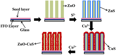
The morphologies of pristine and core–shell heterostructured ZnO NRs are shown in Fig. 1(a) and 1(b), respectively. Fig. 1(a) shows the growth of dense arrays of vertical ZnO NRs of length 400–500 nm and diameter 50–60 nm with a very smooth side wall. On the other hand, Fig. 1(b) (inclined view) shows the core–shell NR arrays, in which it is clearly visible that the side walls of the NRs become rougher due to CuS shell formation. The transmission electron microscopy (TEM) image of a single core–shell NR is shown in Fig. 1(c), which reveals that a ZnO NR core is covered by a CuS shell. The enlarged view of the core–shell NRs (the inset in the corresponding figure) shows that the ZnO core is covered with a continuous layer of CuS shell. The total diameter of a core–shell NR is nearly equal to 70–80 nm. Fig. 1(d) shows the high resolution transmission electron microscopy (HRTEM) images of the interface showing two different lattice fringes of ZnO and CuS crystal structures. The interface between ZnO and CuS is clearly visible (indicated by a white line). The image shows two types of lattice fringes with distances of 0.26 nm, which corresponds to the {0002} plane of wurtzite ZnO, and 0.29 nm for the {10![[1 with combining macron]](https://www.rsc.org/images/entities/char_0031_0304.gif) 2} plane of hexagonal CuS. The inset shows the corresponding diffracted spots of ZnO and CuS. Scanning tunneling electron microscopy (STEM) elemental mapping from the selected area defined by the rectangle in Fig. 1(e) clearly shows the presence of Zn, O, Cu and S elements along a NR. Furthermore, it is clearly evident that the cross-sectional areas of Cu and S are larger than that of Zn, indicating the presence of CuS in the coaxial shell. A schematic diagram has been modeled to show each step for the formation of ZnO–CuS core–shell NR arrays in Fig. 2. The ZnO NR is first transferred to ZnS by the anion exchange process through the replacement of oxygen (O2−) by sulphur (S2−) and then ZnS is gradually transformed to CuS by the cation exchange process. The intermediate steps of formation, phase purity, and crystallographic orientation of the core–shell NR arrays are further confirmed from the results of X-ray diffraction (XRD) analysis (shown in Fig. 3(a)). The XRD pattern of the composite for an intermediate step shows the peaks for ZnS in addition to the wurtzite ZnO peaks. Finally, the diffraction peaks corresponding to the hexagonal covellite structure of CuS along with the wurtzite ZnO ones appear, indicating that the ZnO–CuS core–shell NRs have been successfully synthesized. Furthermore, to confirm the oxidation state of Cu, the X-ray photoelectron spectroscopy (XPS) measurement was done. The XPS spectrum of Cu (2p) (shown in Fig. 3(b)) illustrates two strong peaks at 932 eV and 952 eV, which are assigned to 2p3/2 and 2p1/2. The distinction between CuS and Cu2S is difficult.38 As the Cu-2p photoelectron band exhibits shake-up characteristics on the high binding energy side of the 2p1/2,3/2 doublet for the Cu2+ species, cupric compounds can be easily distinguished from cuprous and pure Cu, both of which lack shake-up peaks . However, for CuS and Cu2S, no shake-up satellites appear in the Cu-2p spectra because of electron orbital interactions.38 The only distinguishing XPS feature is a +0.7 eV shift in the S-2p entroid of CuS vis-à-vis Cu2S. Thus the inset shows that a S-2p peak occurs at 162.6 eV, which confirms the presence of CuS.38
2} plane of hexagonal CuS. The inset shows the corresponding diffracted spots of ZnO and CuS. Scanning tunneling electron microscopy (STEM) elemental mapping from the selected area defined by the rectangle in Fig. 1(e) clearly shows the presence of Zn, O, Cu and S elements along a NR. Furthermore, it is clearly evident that the cross-sectional areas of Cu and S are larger than that of Zn, indicating the presence of CuS in the coaxial shell. A schematic diagram has been modeled to show each step for the formation of ZnO–CuS core–shell NR arrays in Fig. 2. The ZnO NR is first transferred to ZnS by the anion exchange process through the replacement of oxygen (O2−) by sulphur (S2−) and then ZnS is gradually transformed to CuS by the cation exchange process. The intermediate steps of formation, phase purity, and crystallographic orientation of the core–shell NR arrays are further confirmed from the results of X-ray diffraction (XRD) analysis (shown in Fig. 3(a)). The XRD pattern of the composite for an intermediate step shows the peaks for ZnS in addition to the wurtzite ZnO peaks. Finally, the diffraction peaks corresponding to the hexagonal covellite structure of CuS along with the wurtzite ZnO ones appear, indicating that the ZnO–CuS core–shell NRs have been successfully synthesized. Furthermore, to confirm the oxidation state of Cu, the X-ray photoelectron spectroscopy (XPS) measurement was done. The XPS spectrum of Cu (2p) (shown in Fig. 3(b)) illustrates two strong peaks at 932 eV and 952 eV, which are assigned to 2p3/2 and 2p1/2. The distinction between CuS and Cu2S is difficult.38 As the Cu-2p photoelectron band exhibits shake-up characteristics on the high binding energy side of the 2p1/2,3/2 doublet for the Cu2+ species, cupric compounds can be easily distinguished from cuprous and pure Cu, both of which lack shake-up peaks . However, for CuS and Cu2S, no shake-up satellites appear in the Cu-2p spectra because of electron orbital interactions.38 The only distinguishing XPS feature is a +0.7 eV shift in the S-2p entroid of CuS vis-à-vis Cu2S. Thus the inset shows that a S-2p peak occurs at 162.6 eV, which confirms the presence of CuS.38
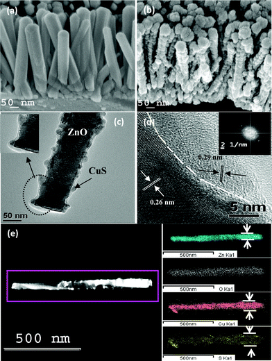 |
| | Fig. 1 (a) FESEM image of the pristine NR arrays. (b) FESEM image of representative core–shell NR arrays. (c) Low-magnification TEM image of ZnO–CuS core–shell NR. Inset: the enlarged view of the core–shell NRs. (d) The magnified HRTEM image of a representative core–shell NR and the inset shows the corresponding FFT pattern. (e) Dark field image of a core–shell NR and STEM mapping of Zn, O, Cu and S elements. | |
 |
| | Fig. 2 Schematic illustration for the summary of the formation processes of ZnO–CuS core–shell NRs arrays step by step. | |
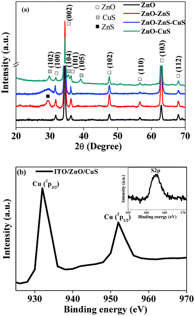 |
| | Fig. 3 (a) XRD analysis of pristine ZnO, ZnO–ZnS, ZnO–ZnS–CuS and ZnO–CuS core–shell composite NR arrays. (b) High-resolution XPS spectra of Cu (2p), S2p (inset). | |
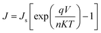
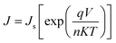
The inset in Fig. 4(a) shows the schematic diagram for the J–V measurements of the heterojunction. The dark J–V curve in Fig. 4(a) exhibits a nice rectifying behavior with a rectification ratio (JF/JR) of ∼60 at 5 V indicating the formation of diode between n-type ZnO core31,39 and p-type CuS shell.40,41 The formation of the n–p heterojunction diode is further confirmed by checking the I–V curves of ITO/ZnO NR and ITO/ZnO/ZnS NR heterostructures (Fig. S1, ESI†), which show linear variation of current with voltage on both sides of zero bias voltage, indicating no junction formation. The turn-on-voltage of the n–p ZnO/CuS core–shell NR array junction is observed to be around 2.3 V. Following the standard diode equation, the current flowing through the junction can be expressed as:
| |  | (1) |
where
J is the current density (obtained by dividing the current value,
I by the area of the diode
A),
V is the voltage across the diode,
Js is the reverse saturation current density,
n is the ideality factor,
T is the temperature in Kelvin, and
q and
K are both constants. For V > 50–100 mV, the −1 term can be ignored and so the above equation can be rewritten as:
| |  | (2) |
 |
| | Fig. 4 (a) Dark J–V characteristics of the ZnO–CuS core–shell heterojunction. Inset: schematic of the layout of the circuit diagram of the n–p heterojunction device on ITO for I–V measurements. (b) Band diagram of the fabricated core–shell heterojunction device on ITO using Au contact. (c) C–V characteristics of the ITO/ZnO/CuS structure at a frequency of 50 kHz. | |
By plotting ln(J) vs. V, the slope gives q/nkT and the intercept gives ln(Js). The values of n and Js obtained for the n-ZnO–p-CuS heterojunction are found to be ∼5.8 and 5.7 × 10⁻⁹ A cm−2, respectively, in voltages ranging from 0.2 to 0.7 V and ∼22.4 and 1.25 × 10⁻⁷ A cm−2, respectively, in voltages ranging from 0.7 to 3.8 V. For an ideal diode, the value of the ideality factor is 1 and it varies from 1 to 2 depending on interfacial layer, barrier height inhomogeneity, or image-force lowering, which is voltage dependent. According to the Sah–Noyce–Shockley theory,42 the values of the ideality factor are around 1.0 at low voltage and up to 2.0 at higher voltages. However, the theoretical model cannot account for the ideality factors greater than 2.0 found in the present study. Therefore, the present value of the high ideality factor can be attributed to the presence of interfacial defect states. The barrier height (φB) is calculated from the equation:
| |  | (3) |
where A
* is Richardson's constant. Considering the theoretical value of A
* as 32 A cm
−2 K
−2,
43φB is calculated to be 0.9 eV and 0.8 eV, respectively, in the voltage ranges 0.2–0.7 V and 0.7–3.8 V. The schematic energy band diagram of the n-ZnO–p-CuS heterojunction is shown in
Fig. 4(b). In the case of n-type ZnO, the band gap energy (
Egn) and electron affinity (
χn) are assumed to be 3.37 eV and 4.2 eV, respectively.
44,45 In the case of p-type CuS (
covellite), the electron affinity (
χp) and the band gap energy (
Egp) are 1.91 eV
46 and 2.2 eV,
47 respectively. There are two energy band offsets due to different electron affinities and band gap values of ZnO and CuS. The conduction band offset (Δ
Ec) is expressed as:
| | | ΔEc = χn − χp = 4.2 − 1.91 = 2.29 eV | (4) |
And the valence band offset (Δ
Ev) is:
| | | ΔEv = Egn − Egp + ΔEc = 3.46 eV | (5) |
A conduction band offset (Δ
Ec) acts as a barrier for the conduction of electrons from n-ZnO to p-CuS. However, the mismatch between the values of
φB and the conduction band offset Δ
Ec (2.29 eV) indicates the presence of an inhomogeneous barrier height (BH). The inhomogeneous BH may be due to various type of defects that could be present at the ZnO–CuS interface. This is quite likely, since chemical conversion of ZnO to ZnS and then to CuS might generate some interfacial defects. The
C–
V characteristics at a frequency of 50 kHz of the ZnO–CuS heterojunction are shown in
Fig. 4(c). It shows that under reverse bias conditions, the capacitance decreases by 22% from 1.50 × 10
−10 F to 1.16 × 10
−10 F for a change in the voltage from 0 to −1.5 V, indicating the presence of interfacial defect states. This is on a par with the
J–
V measurement results.
The semi-log plot of the injection current density for the device with and without UV irradiation (under excitation 365 nm) is shown in Fig. 5(a). The current is increased under reverse bias conditions when UV light (365 nm) is shone on the sample. The analysis of the semi-log plot of the J–V curve under UV illumination shows that the diode still holds a rectifying behavior, however with a lower rectification ratio (JF/JR) of ∼2.5 at 5 V and a turn-on-voltage of 1.2 V. The lower value of JF/JR results from the large increase in current under reverse bias conditions compared to that of the forward bias conditions under UV illumination. The ideality factor n and Js are ∼7 and 7.6 × 10⁻⁷ A cm−2, respectively, in the voltage range 0.2–0.5 V and ∼25 and 8.4 × 10⁻⁶ A cm−2, respectively, in the voltage range 0.5–3.6 V. This is similar to the results shown for the n-ZnO–p-Si junction, where both n and Js increase upon UV illumination.48 It has been found that under UV illumination, the photoconductivity in ZnO NRs is largely dominated by the surface defects,49 and thus the junction behavior deviates much more from the ideal. Our results show that for any voltage under reverse bias conditions, the photo-to-dark current ratio (Iph/Id) is much higher than that of the forward bias conditions, indicating that the n–p junction can act as the photodiode. Fig. 5(b) shows the transient photoresponse characteristics of the ZnO–CuS NR photodiode. The heterojunction can reversibly be turned “on” and “off” in response to the UV light ‘on’ and ‘off’ conditions, respectively. Thus, it is confirmed that the photoresponse of the core–shell NR photodiode is very steady and reproducible and the photocurrent reaches nearly to its saturation value within 10 s. From the enlarged view of a single cycle (shown in Fig. 5(c)), it is clearly observed that the time taken for a 90% current rise (tr) is less than 0.3 s and the time required for the current to fall to 90% is also less than 0.3 s. This value is much shorter than the response times taken by Cu2O–ZnO, Cu4O3–ZnO, and CuO–ZnO photodiodes, which were 1.4, 0.8, and 1.3 s, respectively.50 The shorter response time does not arise from the ZnO NRs alone, since it takes 140 s to reach 90% of its saturation value (photoresponse of ZnO NR arrays is given in Fig. S2, ESI†). The ultrafast UV photoresponse of the core–shell photodiode is very promising for its applications as optical switches.
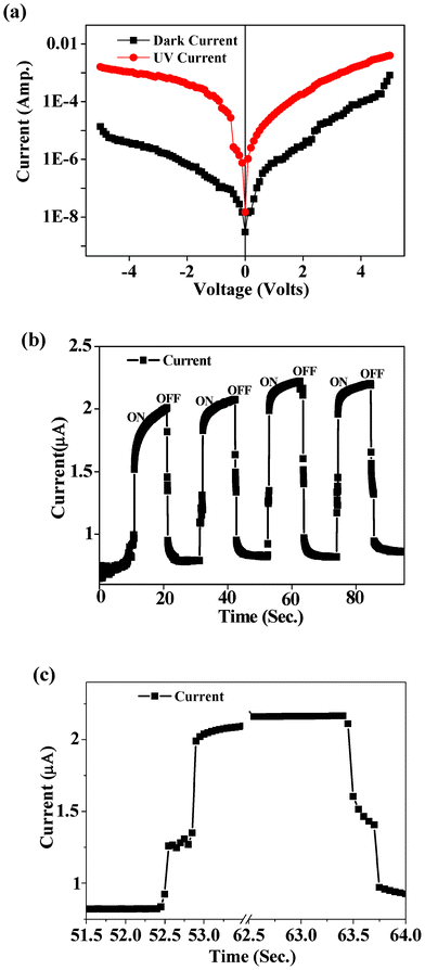 |
| | Fig. 5 (a) Semi-log plots of J–V characteristics measured in the dark and under illumination (365 nm) conditions for the ZnO–CuS core–shell heterojunction. (b) Transient photoresponse by turning UV light on and off for a representative heterojunction. (c) Enlarged part of a transient cycle showing that 90% growth and decay times are faster than 0.3 s. | |
3. Experimental section
Core–shell type ZnO–CuS composite NR arrays were fabricated by a three step chemical method through an ion-exchange route. The strategy for the synthesis of the arrays of ZnO–CuS core–shell NRs is illustrated in Fig. 2. In detail, for the preparation of ZnO NRs, first a ZnO seed layer was grown on the substrate by thermal decomposition of zinc acetate [Zn(CH3COO)2·2H2O] at 350 °C and then the substrates with a seed layer were dipped into an equimolar (20 mM) aqueous solution of zinc acetate [Zn(CH3COO)2·2H2O] and hexamethylenetetramine [(CH2)6N4] at 90 °C for 1 h, followed by a rinsing and drying process. In the 2nd step, to get ZnO–ZnS, the as-prepared NRs were dipped into a solution of thioacetamide (TAA) (Sigma Aldrich) at 70 °C.51 In the last step, when these NRs were dipped into a mixture solution of 25 mM copper acetate [Cu(CH3COO)2·H2O] and 2.5 mM tartaric acid [C4H6O6] at 90 °C, ZnS transforms to CuS by a cation exchange process. For better crystal quality, the as-prepared ZnO–CuS core–shell structured NR arrays were annealed at 500 °C for 60 min under an Ar atmosphere.
The structural characterizations of the pristine and the heterostructured NRs were carried out by X-ray diffractometer (XRD) (model Seifert XDAL 3000). The morphologies were analyzed by field-emission scanning electron microscopy (FESEM, JEOL model JSM-6700F). TEM images were taken on a JEOL-JEM 2010 electron microscope using a 200 kV electron source. TEM images on STEM (HAADF) were taken on a UHR-FEG-TEM, JEOL, JEM 2100 F model using a 200 kV electron source. X-ray photoelectron spectroscopy (XPS, Omicron, model: 1712-62-11) measurement was done using an Al-Kα radiation source under 15 kV voltage and 5 mA current conditions. For J–V measurements, the DC currents were measured between two Au sputtered electrodes (diameter 2 mm) under a certain bias voltage using a Keithley source meter (model 2410). The number of NRs under an Au contact is approximately 4375 × 105, and thus the effective device area is ∼2198 × 10−5 cm2. The dark J–V characteristics were measured after keeping the samples in the dark for several hours. For measuring the J–V curves under illumination conditions, a UV lamp (Spectroline, model: ENF-280C/FE) was shone on the diode from the ITO substrate side. The temporal response of the diode to the UV light was measured by turning the UV light ‘on’ for 10 s and ‘off’ for 10 s periodically and measuring the current under 5 V bias conditions.
4. Conclusions
In summary, we have demonstrated the formation of a ZnO–CuS NR core–shell n–p heterojunction using a facile solution-based cation exchange reaction. The core–shell heterojunction behaves as a rectifying diode, having a rectification ratio of 60. The core–shell junction shows an ultrafast photoresponse speed, indicating its probable application as photodiode. The main advantages of this solution-based method are its simplicity and low cost, which can be exploited to fabricate other n–p core–shell heterojunctions for applications in electronics as well as high-speed electro-optic devices.
Acknowledgements
One of the authors, S. Panigrahi, is thankful to CSIR, New Delhi, for awarding the senior research fellowship. The authors acknowledge the financial support provided through the DST unit of nanoscience at IACS by DST, India.
References
- A. Javey, J. Guo, Q. Wang, M. Lundstrom and H. J. Dai, Nature, 2003, 424, 654–657 CrossRef CAS
 .
.
- X. Wang, J. Zhou, J. Song, J. Liu, N. Xu and Z. L. Wang, Nano Lett., 2006, 6, 2768–2772 CrossRef CAS .
- L. Wang, J. Lian, P. Cui, Y. Xu, S. Seo, J. Lee, Y. Chan and H. Lee, Chem. Commun., 2012, 48, 4052–4054 RSC .
- C. S. Lao, J. Liu, P. X. Gao, L. Y. Zhang, D. Davidovic, R. Tummala and Z. L. Wang, Nano Lett., 2006, 6, 263–266 CrossRef CAS .
- W. I. Park, Y. H. Jun, S. W. Jung and G. C. Yi, Appl. Phys. Lett., 2003, 82, 964–966 CrossRef CAS .
- A. K. Singh and R. Prakash, RSC Adv., 2012, 2, 5277–5283 RSC .
- Q. Qiao, B. H. Li, C. X. Shan, J. S. Liu, J. Yu, X. H. Xie, Z. Z. Zhang, T. B. Ji, Y. Jia and D. Z. Shen, Mater. Lett., 2012, 74, 104–106 CrossRef CAS .
- J. H. He, C. H. Ho and C. Y. Chen, Nanotechnology, 2009, 20, 065503 CrossRef CAS .
- Y. L. Wang, X. C. Jiang and Y. N. Xia, J. Am. Chem. Soc., 2003, 125, 16176–16177 CrossRef CAS .
- Z. Y. Sun, H. Q. Yuan, Z. M. Liu, B. X. Han and X. R. Zhang, Adv. Mater., 2005, 17, 2993–2997 CrossRef CAS .
- X. Dong, Y. Cao, J. Wang, M. B. Chan-Park, L. Wang, W. Huang and P. Chen, RSC Adv., 2012, 2, 4364–4369 RSC .
- K. Keem, J. Kang, C. Yoon, D. Yeom, D.-Y. Jeong, B. Park, J. Park and S. Kim, J. Nanosci. Nanotechnol., 2009, 9, 4240–4243 CrossRef CAS .
- J. B. Cui, R. Sordan, M. Burghard and K. Kern, Appl. Phys. Lett., 2002, 81, 3260–3262 CrossRef CAS .
- Z. Bao, Z. Sun, M. Xiao, L. Tian and J. Wang, Nanoscale, 2010, 2, 1650–1652 RSC .
- J. A. Czaban, D. A. Thompson and R. R. LaPierre, Nano Lett., 2009, 9, 148–154 CrossRef CAS .
- O. Hayden, A. B. Greytak and D. C. Bell, Adv. Mater., 2005, 17, 701–704 CrossRef CAS .
- Z. Sun, Z. Yang, J. Zhou, M. H. Yeung, W. Ni, H. Wu and J. Wang, Angew. Chem., Int. Ed., 2009, 48, 2881–2885 CrossRef CAS .
- S. Panigrahi and D. Basak, Nanoscale, 2011, 3, 2336–2341 RSC .
- C. Gao, X. Li, B. Lu, L. Chen, Y. Wang, F. Teng, J. Wang, Z. Zhang, X. Pan and E. Xie, Nanoscale, 2012, 4, 3475–3481 RSC .
- J. Tang, Z. Huo, S. Brittman, H. Gao and P. Yang, Nat. Nanotechnol., 2011, 6, 568–572 CrossRef CAS .
- T. Gao, Q. H. Li and T. H. Wang, Chem. Mater., 2005, 17, 887–892 CrossRef CAS .
- G. Zhang, W. Wang and X. Li, Adv. Mater., 2008, 20, 3654–3656 CrossRef CAS .
- D. H. Zhang, Z. Q. Liu, S. Han, C. Li, B. Lei, M. P. Stewart, J. M. Tour and C. W. Zhou, Nano Lett., 2004, 4, 2151–2155 CrossRef CAS .
- J. Cao, J. Z. Sun, J. Hong, H. Y. Li, H. Z. Chen and M. Wang, Adv. Mater., 2004, 16, 84–87 CrossRef CAS .
- C. Y. Chen, C. A. Lin, M. J. Chen, G. R. Lin and J. H. He, Nanotechnology, 2009, 20, 185605–185609 CrossRef CAS .
- Z. H. Chen, S. Y. Yeung, H. Li, J. C. Qian, W. J. Zhang, Y. Y. Li and I. Bello, Nanoscale, 2012, 4, 3154–3161 RSC .
- T. Hirakawa and P. V. Kamat, J. Am. Chem. Soc., 2005, 127, 3928–3934 CrossRef CAS .
- A. L. Briseno, T. W. Holcombe, A. I. Boukai, E. C. Garnett, S. W. Shelton, J. J. M. Frechet and P. Yang, Nano Lett., 2010, 10, 334–340 CrossRef CAS .
- J. Xu, X. Yang, H. Wang, X. Chen, C. Luan, Z. Xu, Z. Lu, V. A. L. Roy, W. Zhang and C.-S. Lee, Nano Lett., 2011, 11, 4138–4143 CrossRef CAS .
- J. Yu, J. Zhang and S. Liu, J. Phys. Chem. C, 2010, 114, 13642–13649 CAS .
- R. Ghosh and D. Basak, Appl. Phys. Lett., 2007, 90, 243106–243108 CrossRef .
- Z. Wang, X. F. Qian, J. Yin and Z. K. Zhu, Langmuir, 2004, 20, 3441–3448 CrossRef CAS .
- M. H. Huang, S. Mao, H. Feick, H. Q. Yan, Y. Y. Wu, H. Kind, E. Weber, R. Russo and P. D. Yang, Science, 2001, 292, 1897–1899 CrossRef CAS .
- B. S. Kang, S.-E. Ahn, M.-J. Lee, G. Stefanovich, K. H. Kim, W. X. Xianyu, C. B. Lee, Y. Park, I. G. Baek and B. H. Park, Adv. Mater., 2008, 20, 3066–3069 CrossRef CAS .
- X. Zhao, P. Wang and B. Li, Chem. Commun., 2010, 46, 6768–6770 RSC .
- X. Liu, M. T. Mayer and D. Wang, Appl. Phys. Lett., 2010, 96, 223103–223105 CrossRef .
- R. B. Hall and J. D. Meakin, Thin Solid Films, 1979, 63, 203–211 CrossRef CAS .
-
Corrosion of Electronic and Magnetic Materials, ed. P. J. Peterson, Philadelphia, 1992 Search PubMed .
- G. Kenanakis, D. Vernardou, E. Koudoumas, G. Kiriakidis and N. Katsarakis, Sens. Actuators, B, 2007, 124, 187–191 CrossRef .
- I. Grozdanov and M. Najdoski, J. Solid State Chem., 1995, 114, 469–475 CrossRef CAS .
- S. Inoue, K. Ueda, H. Hosono and N. Hamada, Phys. Rev. B: Condens. Matter, 2001, 64, 245211–245216 CrossRef .
- R. N. N. C-T. SAH and W. Shockley, Proc. IRE, 1957, 45, 1228–1243 CrossRef .
- K. Sarpatwari, O. O. Awadelkarim, M. W. Allen, S. M. Durbin and S. E. Mohney, Appl. Phys. Lett., 2009, 95, 103508–103510 CrossRef .
- P. S. Nayar, J. Appl. Phys., 1982, 53, 1069–1075 CrossRef CAS .
- P. S. Nayar and A. Catalano, Appl. Phys. Lett., 1981, 39, 105–107 CrossRef CAS .
- S. Midda, N. C. Bera, I. Bhattacharyya and A. K. Das, THEOCHEM, 2006, 761, 17–20 CrossRef CAS .
- C. Nascu, I. Pop, V. Ionescu, E. Indrea and I. Bratu, Mater. Lett., 1997, 32, 73–77 CrossRef CAS .
- A. E. Rakhshani, J. Appl. Phys., 2010, 108, 094502–094507 CrossRef .
- S. Panigrahi and D. Basak, Chem. Phys. Lett., 2011, 511, 91–96 CrossRef CAS .
- H. T. Hsueh, S. J. Chang, W. Y. Weng, C. L. Hsu, T. J. Hsueh, F. Y. Hung, S. L. Wu and B. T. Dai, IEEE Trans. Nanotechnol., 2012, 11, 127–133 CrossRef .
- A. Bera and D. Basak, ACS Appl. Mater. Interfaces, 2011, 2, 408–412 Search PubMed .
Footnote |
| † Electronic Supplementary Information (ESI) available. See DOI: 10.1039/c2ra21518g |
|
| This journal is © The Royal Society of Chemistry 2012 |
Click here to see how this site uses Cookies. View our privacy policy here.