CVD-grown TiO2 particles as light scattering structures in dye-sensitized solar cells†
Meysam
Pazoki
ab,
Nima
Taghavinia
*a,
Yaser
Abdi
c,
Fariba
Tajabadi
a,
Gerrit
Boschloo
*b and
Anders
Hagfeldt
b
aPhysics Department, Sharif University of Technology, Tehran, 14588, Iran. E-mail: taghavinia@sharif.edu; Fax: +98 2166164119
bDepartment of Chemistry-Ångström Laboratory, Uppsala University, Box 532 SE 75120, Uppsala, Sweden. E-mail: Gerrit.Boschloo@kemi.uu.se; Fax: +46 184713633
cPhysics Department, Tehran University, Box 6455-14155, Tehran, Iran. Fax: +98 2166164119
First published on 9th October 2012
Abstract
Chemical vapour deposition (CVD) at atmospheric pressure, using TiCl4 as a precursor, was used to grow nanostructured TiO2 films on glass substrates. At relatively low temperatures (∼245 °C) and using relatively high reactant concentrations, different nano-morphologies of TiO2 were formed simultaneously, such as spheres, nanowires and mesoporous structures. The TiO2 spheres were successfully applied as light-scattering particles in dye-sensitized solar cells, either by direct deposition onto electrodes in the reactor, or by preparation of a printing paste from the deposited particles. For dye-sensitized solar cells using the organic dye D35 as sensitizer and a cobalt-complex based redox electrolyte, a solar cell efficiency of 4.4% was obtained using a 5 μm transparent mesoporous TiO2 layer. Addition of a 5 μm light-scattering CVD-particle film increased the efficiency by 22% to 5.4%, which was similar to the result obtained with an equally thick commercially available light-scattering film (5.3%). Longer electron lifetime was found using CVD-based films, which is attributed to the presence of more traps in the bulk of the material.
Introduction
TiO2 thin films and nanostructures are widely used in applications such as self cleaning coatings, photovoltaic solar cells, anti-reflection coatings and the paint industry.1–3 Among the different TiO2 deposition techniques, chemical vapour deposition (CVD) offers several advantages, including purity of coating, moderately low cost, versatility to produce different morphologies, good adhesion to the substrate, and the fact that it is a dry process. Atmospheric pressure CVD grown TiO2 thin films are commercially utilized as self cleaning coatings and as anti-reflection layers on Si solar cells.4 Porous nanostructured TiO2 coatings have attracted enormous attention in the past 20 years, in particular for application in dye-sensitized solar cells (DSC)5 and in photocatalysis.6 In both applications a high surface area is preferred. One-dimensional, oriented structures such as aligned nanowires and nanorods may have advantages over random porous structures in DSCs because of faster electron transport and longer diffusion length.7,8 CVD-grown TiO2 nanowires have only been found in a few investigations.9–16 In this investigation we demonstrate that a simple atmospheric pressure CVD setup can be used to synthesize TiO2 nanostructures with diverse morphologies, including nanowires, under low temperature, high reactant concentration conditions. At relatively low temperatures (∼245 °C) and using relatively high reactant concentrations, different nano-morphologies of TiO2 spheres, nanowires or mesoporous structures were formed simultaneously.DSCs as introduced by O'Regan and Grätzel at 199117 have potential as low cost, environmentally friendly solar cells. They work efficiently under indoor conditions and can be used on flexible substrates.5 Increasing the light harvesting efficiency is one of the subjects that is studied widely for increasing the efficiency of DSCs.5,18,19 The addition of a light-scattering layer on top of a transparent mesoporous TiO2 film increases the optical path length in the film, and thus the photocurrent of the DSC. Specifically, the IPCE is improved in regions where the light absorption by the dye is weak. The light-scattering film is usually composed of a blend of TiO2 particles several 100 nm in size and smaller TiO2 particles (20 nm).
The CVD process introduced here shows promise for new, quick, low-cost and low temperature (<250 °C) growth of TiO2 nanostructures. CVD-grown TiO2 particles can be introduced in two ways for use as light-scattering particles in dye-sensitized solar cells: they can be directly grown on the top of a mesoporous TiO2 film inside the CVD reactor (see the ESI†), or a paste can be prepared from CVD-grown particles and deposited onto mesoporous TiO2 films by printing methods. Using the latter approach, the CVD scattering paste increased the power conversion efficiency of a D35-sensitzed TiO2 solar cell with a cobalt-complex based electrolyte from 4.4% to 5.4%.
Experimental methods
CVD growth of TiO2 nanostructures
The in-house built CVD setup, displayed in Fig. 1, consisted of a horizontal glass tube reactor with 5 cm diameter and 30 cm reactor length. TiCl4 was used as the Ti precursor and oxygen gas and water as the oxygen source. Glass substrates were cleaned by sonication in dilute nitric acid, acetone and deionized (DI) water, and placed in the reactor in three zones A, B and C, separated 3 cm from each other, as shown in Fig. 1. Water vapour and TiCl4 were introduced into the reactor by bubbling Ar and N2 as carrier gases in respective bubblers kept at 20 °C, as well as an independent flow of O2. The standard flow rates for Ar(H2O), N2(TiCl4) and O2 were 30, 560 and 560 sccm, respectively. The standard working temperature of the reactor at the centre (zone C) was 250 °C. The measured temperature in zone B and A was 230 °C and 210 °C, respectively.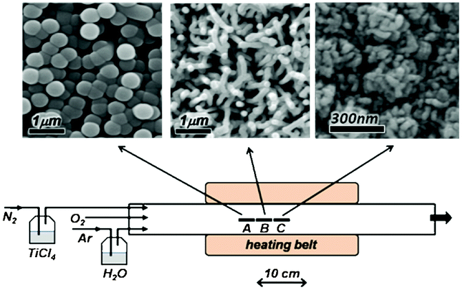 | ||
| Fig. 1 Schematic of the CVD setup, illustrating 3 sample zones, A, B and C separated 3 cm from each other. Zone C is in the centre of the reactor. The corresponding SEM images of the deposited films at each sample zone are shown on top. | ||
CVD-particle based light-scattering paste
The growth of the TiO2 spheres in the CVD reactor was continued for 1 h and finally the powder was collected from the walls of the reactor in region A and used as the material for the CVD light-scattering paste following the procedure of Ito et al.20 The collected TiO2 powder was first dispersed in a 2 M aqueous solution of acetic acid, sonicated with an ultrasonic probe for 2 min and then filtered and dried for use as TiO2 powder for the CVD paste. 6 g of TiO2 powder was mixed and grinded with 1 mL of acetic acid, 1 mL of de-ionized water, 103 mL of ethanol, 20 g of terpineol, 30 g of 10% solution of ethyl cellulose in ethanol, respectively, and the final solution was dried in a rotary evaporator at room temperature for 15 min until a viscous paste was obtained.DSC fabrication
FTO (fluorine doped tin oxide)-coated glass substrates (TEC15, Hartford Glass) were cleaned by immersion in detergent solution, 0.1 M HCl in ethanol, acetone and ethanol in an ultrasonic bath for 20 min, respectively. Between each step the substrates were rinsed with de-ionized water. The FTO substrate was pre-treated in a 40 mM TiCl4 solution at 70 °C for 30 min and washed with DI water. Next, Dyesol DSL 18 NRD-T paste was deposited on the FTO by the screen-printing method. This paste gives transparent mesoporous TiO2 films (T). Two types of light-scattering paste, the CVD paste and the commercial paste PST-400C from JGC Catalysts and Chemicals Ltd (abbreviated here as JGC) containing 400 nm-sized anatase TiO2 microcrystals, were tested. After heating the mesoporous film at 125 °C for 5 min, the light-scattering paste was deposited on top of it. The samples were kept in the ethanol atmosphere for 20 min before heating from 130 to 450 °C in about 2 h. The deposited films used as working electrode were 5 mm × 5 mm in size. The thickness of the films, measured using a profilometer (Veeco Dektak 3), was 5 μm for the transparent mesoporous TiO2 layer and 10 μm for the double layer electrodes (mesoporous film + light-scattering film). The TiO2 films were dye loaded in a 0.2 mM ethanolic solution of D35 ((E)-3-(5-(4-(bis(20,40-dibutoxybiphenyl-4-yl)amino)phenyl)thiophen-2-yl)-2 cyanoacrylic acid) dye overnight, rinsed with ethanol and dried in vacuum. FTO substrates with pre-drilled holes were cleaned as mentioned above, heated for 15 min at 450 °C, coated with one droplet of 5 mM H2PtCl6 ethanolic solution and again heated at 450 °C for 15 min and used as counter electrode. Working and counter electrodes were sealed with 40 micrometre thick thermoplastic frames (Surlyn) and the space between them was filled by electrolyte. The cobalt-based electrolyte used in this work contains 0.22 M Co(bpy)3(PF6)2, 0.05 M Co(bpy)3(PF6)3, 0.1 M LiClO4 and 0.2 M 4-tert butylpyridine in acetonitrile. Silver paint was used for making contacts to the fabricated DSC.Dye adsorption/desorption measurements
N719 dye was absorbed onto TiO2 films from a 0.5 mM ethanolic solution overnight. Dyed films were de-loaded in an aqueous 0.1 M NaOH solution, and the amount of dye was determined spectroscopically (Perkin Elmer Lambda 25). The surface area was calculated assuming that each N719 molecule occupies 1.5 nm2 of surface area.21 A similar procedure was done for the D35 dye, except that here de-loading was done in 3-butyl ammonium hydroxide.Characterization of TiO2 nanostructures
X-Ray diffraction (XRD, Siemens D5000) and scanning electron microscopy (SEM, Hitachi-S4160) was used for characterization of the crystalline phase and surface morphology of the CVD-grown nanostructures and screen printed electrodes. Transmission spectra were recorded using a Cary 5000 spectrometer equipped with an integrating sphere.Solar cell characterization
The current voltages of the DSCs were recorded using a Keithley 2400 source/meter under AM 1.5 G conditions from solar Newport simulator model 91160 calibrated with a certified silicon solar cell. A black mask with a slightly higher area than the active area of the solar cell was used for current–voltage measurements. For measurements in different light intensities, neutral density filters (Thorlabs) were used. The incident photon to current efficiency (IPCE) of the cells was recorded using a xenon light source (Spectral Products ASBXE-175), a monochromator (Spectral Products CM110), and a Keithley 2700 multimeter. Electron lifetime and transport time were recorded by recording the transient of voltage and current of the cell in the response of small amplitude square wave perturbations at different bias light intensities.22 Light was generated by a 1 W white LED (Luxeon) and current and voltage traces were recorded using a current amplifier (SRS 570) and a digital data acquisition board (National Instruments). The amount of extracted charge at open circuit and short circuit conditions were measured by biasing the LED light, keeping the cell in the desired working condition for 10 s and finally turning the light off and integrating current versus time for 15 s. The short circuit Fermi level was measured by a method introduced elsewhere.23 Electrochemical impedance spectroscopy of the solar cells was measured using an Autolab PST100N electrochemical interface and data was analyzed using Zview 2.0 software.Results and discussions
CVD of TiO2 nanostructured films
The TiO2 films grown in different zones of the reactor differ much in morphology, as shown in Fig. 1. In zone A, the films consist of close-packed spherical particles, while in zones B and C nanowires and mesoporous morphologies appear. All structures are composed of TiO2. X-Ray diffraction analysis showed that as prepared films are predominantly amorphous, with the exception of the mesoporous nanostructures that display the anatase structure. After annealing in air at 450 °C, all samples show anatase diffraction peaks, see the ESI.†It is noted that the distance between zones A–C is small and that the growth is sensitive to the precise position of the substrates. Careful control (cleanliness of the reactor, exact flow regulation and temperature settings, exact positioning of substrates) is essential to obtain reproducible results.
The morphological difference of the TiO2 nanostructures in zones A–C can be explained by differences in temperature, reactant concentrations and gas boundary conditions.24 A general description of the factors responsible for differences in growth is given in the ESI.†
In zone A, nearly mono-disperse, spherical particles with an average size of 450 nm are deposited on the substrate. These spheres are most likely formed in the gas phase, and subsequently deposited on the substrate. The high concentration of reactants in zone A (close to the inlet of reactants), compared to zones B and C, favors gas phase nucleation and the growth of TiO2 particles over surface growth. The gas phase growth of TiO2 spherical nanoparticles has been reported in low pressure reactors (∼mbar), resulting in particles of about 10 nm size.12,13 The higher pressure in our case is expected to considerably decrease the mean free path of monomers and increase the monomer collision rate as well as the residence time in the reactor, leading to the formation of larger particles.
The diameter of the spheres can be tuned by the temperature and partial pressure of reactants (see section S2 in the ESI†). Decreasing the temperature and increasing the flow rate of reactants leads to larger particle sizes, in good agreement with other work25,26 and can be explained by reaction–coagulation–sintering model.27
The specific surface area of annealed nanostructured films deposited in different positions in the CVD reactor was obtained by dye adsorption/desorption measurements using the dye N719 and by weighing the mechanically removed film.28 The specific surface area of the spherical particle film was determined as 3.6 m2 g−1. The average particle size observed by SEM was 450 nm under the conditions used. Using this value a theoretical surface area S can be calculated using S = 6/ρd, with d the particle diameter and ρ the density of the pure material (3.84 g cm−3 for TiO2 anatase), yielding a value of 3.5 m2 g−1, in good agreement with the experimental value. This suggests that these particles are non-porous.
The spherical particles are most likely formed in the gas phase and subsequently deposited on the substrate. There are some indications that indicate some further growth takes place on the substrate: the fact that particles are highly packed in some areas of the film, and that the shape of some particles is distorted in order to accommodate close packing, suggests that particles have a degree of flexibility, when they are deposited. It was also observed that the thickness of the particle film does not increase beyond a certain value (∼4 μm), even though more particles are formed and found in other parts of the reactor. More study on the nature and precise control of particle deposition is required.
In zone B, TiO2 nanowires of ∼150 nm in diameter and ∼2 μm in length are formed. The growth rate is rather high: ∼200 nm min-1. The active surface area, measured by dye loading, for 1 cm2 of a 2 μm-thick film, was 21.9 cm2. The estimated roughness factor of cylindrical wires of 150 nm diameter and 2 μm length with 2.3 × 10⁹ wires cm−2 (estimated from SEM pictures) is 22 cm2 cm−2, which is close to the measured value, and suggests that the wires are not porous inside. Most wires are oriented perpendicular to the substrate. The reason for the asymmetric growth of TiO2 in the form of wires is unclear. Upon close inspection of the SEM images it was found that some nanowires combine together at the top and make a single nanowire, growing from the intersection point (Fig. 2a). This implies that the nanowires grow from the tip. Furthermore, most wires have spherical particles on top and show some radial distortions in the whole area around the diameter, giving it a worm-like appearance (Fig. 2b).
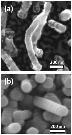 | ||
| Fig. 2 High resolution SEM pictures of CVD-grown TiO2 nanowires. (a) Nanowires combining on top to a single nanowire. This shows that the growth continues from the top. (b) Vertical growth of wires with a spherical tip and radial rings on the diameter. | ||
In zone C, at the centre of the reactor, the temperature is higher than in zones A and B, while the reactant concentration is lower. Here, clumps of aggregated nanoparticles are deposited, forming a mesoporous TiO2 structure, giving a uniform coverage of substrate and yielding films with high surface area. For a film of 200 nm thickness, the roughness factor was determined to be 83 cm2 cm−2 using the dye loading measurement. This is about 40 times higher than nanowire films of the same thickness. The film has features of ∼30 nm size in the SEM micrograph (Fig. 1), but the high roughness factor suggests that the actual particle size must be less than 10 nm. The growth rate of these structures is very low: a few nanometres per minute. Unlike the particle and wire films, the as-grown structures are crystalline with the anatase phase. The low growth rate, plus the strong adhesion of the films to the substrate, demonstrates that the films grow on the substrate by the surface-based CVD process.
CVD-based light-scattering films in dye-sensitized solar cells
Light-scattering films can be grown directly onto mesoporous TiO2 electrodes by CVD, see the ESI† section S3. This procedure was successful, but quite tedious, and in the remainder of this work we will describe results obtained with screen-printing paste prepared from CVD-grown particles.In Fig. 3 SEM micrographs of CVD and JGC light-scattering films are shown. The films prepared using CVD-particles (collected from zone A) have bigger particles and also have bigger holes compared to the JGC film. Both electrodes consist of a mix of big particles that act as light scatterers, and smaller particles that are required for a good connection between all particles. The latter also increases the surface area of the resulting electrodes. Fig. 4 shows the XRD pattern of a sintered light-scattering CVD film. The phase of the TiO2 particles was mainly anatase, but there is also a small fraction of rutile particles. The anatase crystallite size of the CVD paste, calculated using the Debye–Scherrer formula, was 10.7 nm. This suggests that the large particles observed in SEM are aggregates built up from much smaller crystals. This is confirmed by high resolution SEM (see Fig. S3 in the ESI†). Raman spectra of the large particles display anatase peaks (Fig. S4 in the ESI†). From the full width at half maximum of the Eg1 peak a crystallite size of about 14 nm was determined.1 X-Ray photoelectron spectroscopy (XPS) spectra of the CVD films suggest pure TiO2 material, e.g., no nitrogen peaks were found (see Fig. S5 in the ESI†).
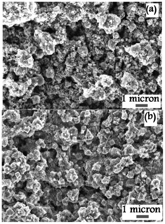 | ||
| Fig. 3 SEM pictures of the light-scattering TiO2 films (a) prepared from CVD particles and (b) JGC_PST-400C. | ||
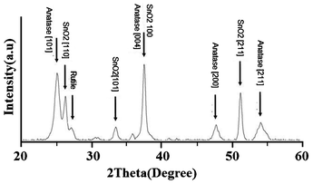 | ||
| Fig. 4 The XRD pattern of the sintered CVD light-scattering film. | ||
Fig. 5 shows the total transmission spectra of the different TiO2 films on the FTO substrates. The transparent film shows a high transmittance of about 82%. Addition of the CVD scattering layer decreased the transmittance to 33% in the 600 to 700 nm wavelength range, while addition of the JGC layer lowered the transmittance to about 22%. Since TiO2 is not absorbing light at these wavelengths, the decrease in transmittance is directly attributed to the light-scattering properties of the CVD and JGC films. This is confirmed by the pure white appearance of these films. The total reflectance at these wavelengths is thus 67% and 78% for the CVD and JGC film, respectively.
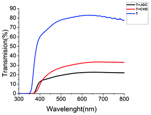 | ||
| Fig. 5 Total (specular + diffuse) transmission of T, T + CVD and T + JGC films on TEC15 substrates. | ||
Fig. 6 and Table 1 show the IV curves and characteristics for fabricated DSCs comparing the effect of the CVD paste and JGC paste as scattering layers. T, T + CVD and T + JGC are representative of DSCs with 1 layer of transparent Dyesol paste, 1 layer of Dyesol paste plus 1 layer of CVD paste, and 1 layer of Dyesol paste plus 1 layer of JGC_PST-400C scattering paste, respectively. Addition of a light-scattering layer improved the current density and the overall efficiency of the solar cells. The T + CVD has slightly better power conversion efficiency in comparison to T + JGC. The main difference between T + CVD and T + JGC is the better fill factor of the former. The short circuit current varies linearly with light intensity (see Fig. S8 of the ESI†), demonstrating that the mass transport of cobalt mediators in the electrolyte is not limited by film thickness or porosity.
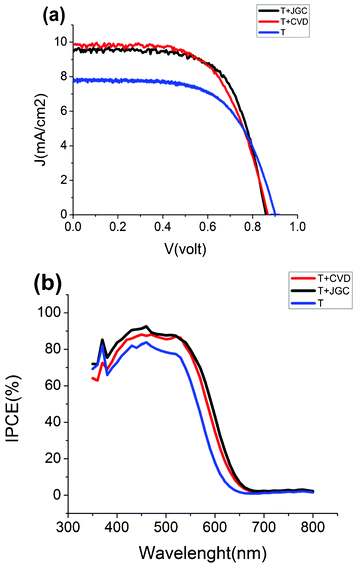 | ||
| Fig. 6 (a) Current–voltage characteristics of D35-sensitized solar cells with cobalt tris-bipyridine based electrolyte, with 5 μm transparent TiO2 (T), T plus 5 μm CVD-based TiO2 (T + CVD), and T plus 5 μm JGC-based TiO2. (b) IPCE spectra of the same solar cells. | ||
Fig. 6b shows the IPCE spectra of DSCs with and without scattering layers. The IPCE is increased by the presence of the light-scattering film, due to the increased overall thickness of the electrode as well as the significantly improved light scattering, which will reflect light back into the transparent TiO2 part of the electrode. In red region T + JGC has a slightly better IPCE than the CVD paste. Dye adsorption/desorption experiments showed a slightly higher amount of adsorbed dye for the T + JGC films (∼8% more than for T + CVD), see Table 1. The enhancement of the photocurrent due to the light-scattering layer was much more pronounced for solar cells sensitized with N719, which has a broader spectrum and a lower extinction coefficient than D35. See the ESI† section S3 for IV curves and further information.
Electron transport, recombination and accumulation in the different solar cell devices were investigated using light modulation techniques.22,23Fig. 7 shows the results of the electron transport time and the electron lifetime. The electron lifetime in devices with the CVD scattering paste was longer than in devices with the JGC films. At the open circuit voltage (870 mV) of the T + JGC cell, the electron lifetime was 11 milliseconds but in the T + CVD cell at the open circuit voltage (860 mV) it was 22 milliseconds. The longer electron lifetime of the T + CVD cell implies a slower recombination of electrons and is likely to contribute to a higher fill factor in the solar cell. Also the presence of larger pores in the CVD film can improve the diffusion of cobalt redox mediators inside the electrode leading to the enhancement of the fill factor of the T + CVD cell.
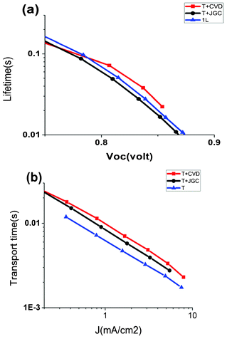 | ||
| Fig. 7 (a) Electron lifetime as a function of the open-circuit potential. (b) Electron transport time as a function of the short-circuit photocurrent of the fabricated solar cells. | ||
As expected, the electron transport time is shortest in devices with the thinnest TiO2 film, i.e. device T. There were some differences between the T + JGC and T + CVD devices, where electron transport was 20% faster in T + JGC.
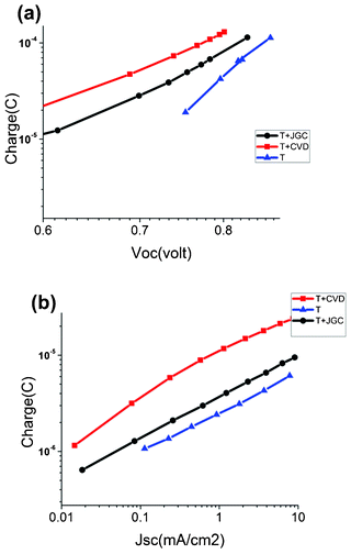
Charge extraction experiments were performed from open circuit and short circuit solar conditions to determine the amount of charge stored in the different TiO2 films, see Fig. 8. In device T the lowest amount of charge is found, which is expected on the basis of the thinnest TiO2 layer. Addition of a scattering layer doubles the accumulated charge at a given voltage (Fig. 8a) for the T + CVD device, while the increase in charge is less for the T + JGC device. We attribute the presence of a larger number of trap states in the CVD film to the polycrystalline nature of the large light-scattering aggregates, compared to the JGC film that has large single crystalline scattering particles.
 | ||
| Fig. 8 Extracted charge from (a) open circuit and (b) short circuit conditions. | ||
The larger amount of trap states in the CVD film is also evident from the extracted charge under short-circuit conditions (Fig. 8b), where the charge is about two times larger for T + CVD compared to T + JGC at the same current density.
The exponential behaviour of the charge versus open circuit voltage is consistent with an exponential distribution of trap states below the conduction band edge. For a trap distribution g(V) = g0exp(V/m), the density of trap states nt is given by: 7
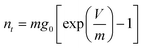 | (1) |
The recombination resistance and chemical capacitance of the cells was studied with electrochemical impedance spectroscopy (EIS) in the dark at an applied potential of 0.85 V. Fig. 9 shows the Bode plots of the measured data, along with the fitted curves. The high-frequency part is nearly identical for all devices. This part is attributed to the resistance and capacity of the counter electrode–electrolyte interface. The low-frequency part differs, and is dominated by the recombination resistance (Rrec) and chemical capacitance (CTiO2) of the porous TiO2 electrode. As expected Rrec is smaller for the thinnest electrode (T). The model developed by Fabregat-Santiago et al. was used for fitting and interpretation of the EIS data.29
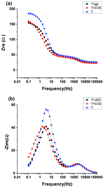 | ||
| Fig. 9 Real and imaginary part of the impedance as a function of the frequency for the different devices. The points show the measured data and the solid lines show the fitted curves. | ||
The fitted values presented in Table 3 show that both the recombination resistance and the chemical capacitance is higher in T + CVD than in the T + JGC device, resulting in a higher electron lifetime (= Rrec × CTiO2) in these cells. The determined electron lifetimes from the EIS data recorded in the dark were systematically higher than the lifetimes from the photoinduced voltage transient measurements. This can be attributed to the fact that under illumination there is additional recombination to oxidized dye molecules. Furthermore, the local concentration of Co(III) species will be higher than under dark conditions. Finally, there are slight differences in the Fermi-level in the porous TiO2 under the different conditions.
The trend in the capacitances agrees with that found with charge extraction data at the open circuit (Fig. 8a). The large CTiO2 for T + CVD is attributed to large density of bulk traps. These traps will not contribute to recombination. This is consistent with the fact that the recombination resistance of T + CVD is decreased compared to T, but much less than the decrease for T + JGC.
Conclusions
A simple atmospheric pressure chemical vapour deposition setup was used to grow simultaneously different TiO2 morphologies on glass substrates. Using TiCl4, O2 and H2O as reactants, rapid film growth at relatively low temperature (250 °C) was obtained. Depending on the zone in the hot-wall reactor, spherical particles, nanowires and mesoporous structures were found, due to local differences in temperatures, reactant concentrations, and boundary layer conditions.CVD grown TiO2 spheres are efficient for use as scattering structures in DSCs. The scattering properties of electrodes prepared using CVD-grown particle paste were found to be similar to that of JGC_PST-400C paste and resulted in similar solar cell efficiencies. The presence of bulk traps in the CVD particles, probably related to the small grains from which they are composed, resulted in a higher trap density in the electrodes with these particles, but this did not have a detrimental effect on the solar cell performance. Using the CVD scattering paste with cobalt-based electrolyte and D35 dye improved the efficiency of a 5 μm thick transparent mesoporous TiO2 from 4.4% to 5.4%. The CVD growth of micrometre TiO2 spheres is a very quick and low cost method for the fabrication of efficient scattering particles for DSCs.
The temperature for the deposition of the scattering layer was as low as 250 °C, which may be compatible with plastic substrates. This suggests that full CVD processes may be designed for the fabrication of the mesoporous photoanode of dye-sensitized solar cells.
Acknowledgements
The Iran Ministry of science and technology, the Swedish Research Council (VR), and the STandUP for energy program are thanked for financial support. We thank JGC Catalysts and Chemicals Ltd for their generous gift of PST-400C paste and Amin Pourandarjaani and Shabnam Dadgostar for their help in the CVD work and Roghayeh Imani for Raman analysis.References
- X. Chen and S. Mao, Chem. Rev., 2007, 107, 2891 CrossRef CAS
.
- D. V. Bavykin, J. M. Friedrich and F. C. Walsh, Adv. Mater., 2006, 18, 2807 CrossRef CAS
- B. O'Regan and D. T. Schwartz, Chem. Mater., 1998, 10, 1501 CrossRef CAS
- B. S. Richards, S. F. Rowlands, C. B. Honsberg and J. E. Cotter, Progr. Photovolt.: Res. Appl., 2003, 11, 27–32 CrossRef CAS
- A. Hagfeldt, G. Boschloo, L. Sun, L. Kloo and H. Pettersson, Chem. Rev., 2010, 110, 6595 CrossRef CAS
- H. Tong, S. Ouyang, Y. Bi, N. Umezawa, M. Oshikiri and J. Ye, Adv. Mater., 2012, 24, 229 CrossRef CAS
- R. Mohammadpour, A. Iraji zad, A. Hagfeldt and G. Boschloo, ChemPhysChem, 2010, 11, 2140 CrossRef CAS
- X. Feng, K. Shankar, O. K. Varghese, M. Paulose, T. J. Latempa and C. A. Grimes, Nano Lett., 2008, 8, 3781 CrossRef CAS
- J. Lee, K. Park, T. Kim, H. Choi and Y. Sung, Nanotechnology, 2006, 17, 4317 CrossRef CAS
- J. Wu, H. C. Shih and W. Wu, Chem. Phys. Lett., 2005, 413, 490 CrossRef CAS
- J. Lee, Y. Sung, T. Geun Kim and H. Choi, Appl. Phys. Lett., 2007, 91, 113104 CrossRef
- J. Wu, H. C. Shiha and W. Wu, Nanotechnology, 2006, 17, 105 CrossRef CAS
- H. Liu, Y. Zhang, R. Li, M. Cai and X. Sun, J. Nanopart. Res., 2010, 13, 385 CrossRef
- J. Wang, L. Zhao, V. S.-Y. Linb and Z. Lin, J. Mater. Chem., 2009, 19, 3682 RSC
- J. Wu and C. Yu, J. Phys. Chem. B, 2004, 108, 3376 Search PubMed
- C. A. Chen, A. Korotcov, Ying-Sheng Huang, W. H. Chung, D. S. Tsai and K. K. Tiong, J. Mater. Sci.: Mater. Electron., 2009, 20, 332 CrossRef CAS
- B. O'Regan and M. Grätzel, Nature, 1991, 353, 737 CrossRef CAS
- S. Hore, C. Vetter, R. Kern, H. Smitc and A. Hinsch, Sol. Energy Mater. Sol. Cells, 2006, 90, 1176 CrossRef CAS
- F. Huang, D. Chen, X. Zhang, R. A. Caruso and Y. Cheng, Adv. Funct. Mater., 2010, 20, 1301 CrossRef CAS
- S. Ito, P. Chen, P. Comte, M. Nazeeruddin, P. Liska, P. Pechy and M. Gratzel, Progr. Photovolt.: Res. Appl., 2007, 15, 603 CrossRef CAS
- M. Zukalova, J. Prochazka, A. Zukal, J.-H. Yum and L. Kavan, Inorg. Chim. Acta, 2008, 361, 656 CrossRef CAS
- G. Boschloo, L. Häggman and A. Hagfeldt, J. Phys. Chem. B, 2006, 110, 13144 CrossRef CAS
- G. Boschloo and A. Hagfeldt, J. Phys. Chem. B, 2005, 109, 12093 CrossRef CAS
-
H. O. Pierson, Handbook of chemical vapor deposition, Noyes publication, New Jersey, 1999, ch. 2, pp. 46–50 Search PubMed
- K. Akurati, S. S. Bhattacharya, M. Winterer and H. Hahn, J. Phys. D: Appl. Phys., 2006, 39, 2248 CrossRef CAS
- K. Nakasoa, K. Okuyama, M. Shimada and S. E. Pratsinis, Chem. Eng. Sci., 2003, 58, 3327 CrossRef
-
M. Winterer, Nanocrystalline ceramics synthesis and structure, Springer, Berlin, 2002, ch. 2, pp. 30–33 and 45–47 Search PubMed
- L. Shooshtari, M. Rahman, F. Tajabadi and N. Taghavinia, ACS Appl. Mater. Interfaces, 2011, 3, 638 CAS
- F. Fabregat-Santiago, J. Bisquert, G. Garcia-Belmonte, G. Boschloo and A. Hagfeldt, Sol. Energy Mater. Sol. Cells, 2005, 87, 117–131 CrossRef CAS
Footnote |
| † Electronic Supplementary Information (ESI) available: See DOI: 10.1039/c2ra21361c |
| This journal is © The Royal Society of Chemistry 2012 |