Controlled growth and up-conversion luminescence of Y2O2S![[thin space (1/6-em)]](https://www.rsc.org/images/entities/h2_char_2009.gif) :Er3+ phosphor with the addition of Bi2O3
:Er3+ phosphor with the addition of Bi2O3
Xuanshun
Wu
a,
Huidan
Zeng
*a,
Qing
Yu
a,
Chaxing
Fan
a,
Jing
Ren
a,
Shuanglong
Yuan
*a and
Luyi
Sun
b
aKey Laboratory for Ultrafine Materials of Ministry of Education, School of Materials Science and Engineering, East China University of Science and Technology, Shanghai 200237, China
bDepartment of Chemistry and Biochemistry & Materials Science and Engineering Program, Texas State University–San Marcos, San Macros, TX 78666, USA. E-mail: hdzeng@ecust.edu.cn; shuanglong@ecust.edu.cn
First published on 20th August 2012
Abstract
By adding Bi2O3 in phosphor raw materials, fine particles (ca. 500 nm in diameter) have been synthesized for the first time in Y2O2S![[thin space (1/6-em)]](https://www.rsc.org/images/entities/char_2009.gif) :Er3+via high-temperature solid-state reaction. The influence of Bi2O3 content on the crystal growth and up-conversion (UC) luminescence (excited at 1550 nm) of Y2O2S:Er3+ phosphors was investigated by varying the Bi2O3 concentration from 0 to 10.0 mol%. As Bi2O3 concentration was increased, the average particle size was increased and then decreased, and the uniformity of the particle size was descended and then enhanced. The size change of Bi2O3 doped Y2O2S:Er3+ phosphors can be well explained by the liquid phase sintering mechanism. Compared to the phosphors without containing any Bi2O3, UC luminescence intensity (excited at 1550 nm) of phosphors containing Bi2O3 decreased, but was still sufficiently strong to the naked eye.
:Er3+via high-temperature solid-state reaction. The influence of Bi2O3 content on the crystal growth and up-conversion (UC) luminescence (excited at 1550 nm) of Y2O2S:Er3+ phosphors was investigated by varying the Bi2O3 concentration from 0 to 10.0 mol%. As Bi2O3 concentration was increased, the average particle size was increased and then decreased, and the uniformity of the particle size was descended and then enhanced. The size change of Bi2O3 doped Y2O2S:Er3+ phosphors can be well explained by the liquid phase sintering mechanism. Compared to the phosphors without containing any Bi2O3, UC luminescence intensity (excited at 1550 nm) of phosphors containing Bi2O3 decreased, but was still sufficiently strong to the naked eye.
1. Introduction
Er3+ doped up-conversion (UC) materials have recently attracted considerable attention for their valuable applications in solid state visible lasers, color displays, and biomedical imaging.1–3 It is well known that Y2O2S:Er3+ is one of the most popular UC phosphors, because it exhibits excellent chemical stability, high luminescent efficiency, and moderate phonon energies (about 520 cm−1).4
Currently, the high-temperature solid-state reaction is the main method to prepare rare earth oxysulfide phosphors, which use, e.g. Na2CO3, as flux for their low cost and high operability. However, the phosphors prepared via this method exhibit a large particle size in micron range,5,6 which significantly narrows their applications. Therefore, it is highly desirable to decrease the average particle size.
Several approaches have been developed to prepare fine phosphors, including co-precipitation method, sol–gel method, combustion method, hydrothermal method, etc.7–9 However, such approaches have been rarely used in commercial production of fine phosphors because of their long manufacturing duration, high cost, and complex operability.
Alternatively, one may use crystal growth inhibitors to lower crystal size. For example, an appropriate liquid phase can be applied to restrain crystal growth. The presence of a liquid phase during sintering can induce the transition from normal to anomalous grain growth. In order to apply liquid phase successfully during sintering of Y2O2S and optimize microstructural evolution, the concentration of liquid phase in the sample during sintering must be carefully tuned. Bi2O3, which has a low melting point of 700 °C, has been reported to help reduce crystal size of ceramics.10–12 In this paper, we also choose Bi2O3 as a potential crystal growth inhibitor to decrease crystal size. All Y2O2S:Er3+ samples were prepared by high-temperature solid-state reaction method. The aim of this work is to study the influences of Bi2O3 concentration (varying from 0–10.0 mol%) on the crystal growth, crystal size uniformity, and UC luminescence properties of Y2O2S:Er3+ phosphors.
2. Experimental
2.1 Samples preparation
(Y0.95Er0.05)2O2S–xBi2O3 (x = 0, 1.0, 3.0, 5.0, 7.0, 10.0 mol%) phosphors were prepared by high-temperature solid-state reaction method. High-purity power of Y2O3 (99.99%), Er2O3 (99.99%) and S (99.999%), Na2CO3 and Bi2O3 (all analytical reagents) were used as raw materials. Both Na2CO3 and S were added from 30.0 to 50.0 wt%. All chemicals were mixed and then sintered at 1100 °C for 3 h using alumina crucibles with alumina covers in carbon reducing atmosphere. The sintered samples were further treated by washing with dilute hydrochloric acid and distilled water several times. The washed powders were subsequently filtered and dried.2.2 Material characterization
The phosphor samples were characterized by X-ray diffraction (XRD) (Rigaku, D/Max-RB, Cu-Kα radiation, λ = 0.15406 nm). The morphology of the phosphor samples were examined by a field emission scanning electron microscope (FE-SEM, S-4800, Hitachi High-Technologies). Absorption spectra of the samples were measured by a UV-Vis-NIR spectrophotometer (CARY 500, Varian Company, America) equipped with an integrating sphere, and the samples to be measured were put in the same sample pool and then pressed to the same thickness. The UC luminescence spectra were recorded at room temperature on an Edinburgh FLS920P spectrometer, excited by a power tunable 1550 nm semiconductor laser diode (0–500 mW). All measurements were performed under the same conditions.3. Results and discussion
3.1 Influence of Bi2O3 concentration on the crystal growth of Y2O2S![[thin space (1/6-em)]](https://www.rsc.org/images/entities/h3_char_2009.gif) :Er3+ phosphors
:Er3+ phosphors
The XRD patterns of the as-obtained samples with various Bi2O3 concentrations are shown in Fig. 1. According to XRD patterns, the phases of the samples are hexagonal Y2O2S (JCPDS # 24-1424) and a small amount of orthorhombic Bi2S3 impurity (JCPDS # 65-3884). Increasing Bi2O3 concentration from 0 to 10.0 mol% had virtually no effect on the XRD patterns of the samples. In Fig. 1(b)–(c), the XRD patterns of the samples do not reveal the presence of any additional phase other than hexagonal Y2O2S. However, in Fig. 1(d)–(g), a very weak peak of orthorhombic Bi2S3 phase appears for the samples with x > 1.0 mol% Bi2O3 additives. The intensity of Bi2S3 phase peak increases slightly with increasing concentration of Bi2O3.
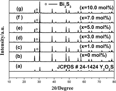 | ||
| Fig. 1 XRD patterns of samples (Y0.95Er0.05)2O2S–xBi2O3 and reference date JCPDS # 24-1424. | ||
The crystal symmetry of Y2O2S is hexagonal with space group P-3ml. There is one formula unit per unit cell. The structure is very closely related to the A-type rare-earth oxide structure, with the difference being that one of the three oxygen sites is occupied by a sulfur atom.6 The formation of orthorhombic Bi2S3 phase indicates that partial Bi ions can participate in the reaction with S ions to form Bi2S3 during sintering process. When Bi2O3 concentration is low, the amount of Bi2S3 impurity is too low to be detected by the XRD measurement. However, as the concentration of Bi2O3 increased, the diffraction intensity of the orthorhombic Bi2S3 phase increased continually. But overall, the diffraction intensity of the Bi2S3 phase peak is very weak compared with the main peak (101) of Y2O2S phase, suggesting that the amount of Bi2S3 phase is marginal. To confirm the existence of Bi2S3 impurity, the x = 10.0 mol% sample was further treated by washing with dilute FeCl3 solution, and the diffraction peak at 28.5° disappeared, which supports the above hypothesis.
The SEM images of (Y0.95Er0.05)2O2S–xBi2O3 (x = 0, 1.0, 3.0, 5.0, 7.0, 10.0 mol%) samples are shown in Fig. 2. All samples exhibit hexagonal morphology. It is also found that Bi2O3 additive influences grain growth. The observed average particle size for Y2O2S:Er3+ sample without Bi2O3 is about 2 μm (Fig. 2(a)). The addition of Bi2O3 significantly changes the microstructure. The main feature of the sample with the lowest concentration of Bi2O3 was significantly increased grain size (Fig. 2(b)). The addition of a higher concentration of Bi2O3 caused a decrease in particle size (Fig. 2(c)–(f)). From Fig. 2(f), one can find that the sample with 10.0 mol% Bi2O3 concentration is the best in terms of uniformity and average size (ca. 500 nm in diameter).
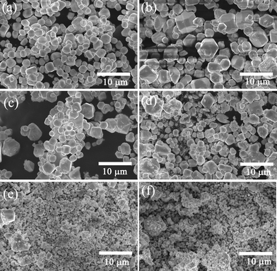 | ||
| Fig. 2 SEM images for (Y0.95Er0.05)2O2S–xBi2O3 (x = 0, 1.0, 3.0, 5.0, 7.0, 10.0 mol%) samples: (a) x = 0 mol%, (b) x = 1.0 mol%, (c) x = 3.0 mol%, (d) x = 5.0 mol%, (e) x = 7.0 mol%, (f) x = 10.0 mol%. | ||
Bi2O3 is a low melting point additive whose melting point is 700 °C. During sintering, it forms a liquid phase and influences the grain growth of Y2O2S. Thus, the sintering kinetics would be determined by the liquid phase sintering due to sintering temperature of 1100 °C. It can be postulated that grain growth mechanisms relating to Y2O2S were rate controlling, depending on the amount of Bi2O3 liquid phase: (i) solution-re-precipitation process—a thin layer of Bi2O3-rich liquid phase is needed; (ii) diffusion of atoms through the Bi2O3-rich liquid phase.13 During the grain growth of Bi2O3 added Y2O2S, the above two types are clearly identified in the regions with x = 0 or 1.0 mol% and x > 1.0 mol%, respectively.
The microstructural development of Y2O2S doped with Bi2O3 liquid phase can be discussed by the application of the generally accepted grain growth kinetics represented by the following relation:14
| Dmn − D0n = k0t exp (−Q/kT) | (1) |
The grain growth mechanism of Y2O2S doped with 1.0 mol% concentration of Bi2O3 can be explained by the application of the well accepted liquid phase sintering mechanism which is a solution-reprecipitation process.15 During the formation of giant grains, the smallest grains, which are thermodynamically less stable, dissolve in the liquid phase and subsequently precipitate on the larger grains and/or the more curved part of the grain dissolves and precipitates on less curved grain boundaries. The grain growth rate of Y2O2S in the presence of liquid phase is controlled either by the solid–liquid phase boundary reaction or by diffusion through the liquid phase from smaller grains to larger grains. Thus, the dramatic decrease of the activation energy for grain growth (dramatic increase of grain size) in the sample (x = 1.0 mol%) and the high solubility of Y2O2S in Bi2O3 lead to an intense solid-liquid phase boundary reaction, which causes the anomalous grain growth. Moreover, the x = 1.0 mol% sample exhibits a structure of poor uniformity. The discontinuous grain growth probably indicates an inhomogeneous distribution of the liquid phase owing to the low concentration of Bi2O3 liquid phase.
The liquid phase layer not only accelerates mass transfer but also forms wetting menisci at the grain boundaries, providing an additional capillary pressure driving force for sintering.16 Up to a higher concentration (x > 1.0 mol%), the thickness of the liquid phase layer increases with increasing Bi2O3 concentration. Thus the sintering mechanism is the diffusion of atoms through the Bi2O3-rich liquid phase. The grain growth rate for the liquid phase–boundary reaction controlled process is not dependent on the amount of liquid phase, which can be explained by the following formula:17
| dG/dt = KVmf/kT | (2) |
| dG/dt = 2DSMσ/kTρδ (G/G0−1) | (3) |
3.2 Influence of Bi2O3 concentration on the UC luminescence of Y2O2S:Er3+ phosphors
Absorption spectra of the samples with various Bi2O3 concentrations are shown in Fig. 3. The high-energy bands at wavelength shorter than 240 nm in the absorption spectra resulted from the fundamental absorption of the Y2O2S host lattice. The sharp absorption bands can be attributed to the following transitions 4G11/4→4I15/2 (381 nm), 4F7/2→4I15/2 (495 nm), 2H11/2→4I15/2 (524 nm), 4F9/2→4I15/2 (661 nm), 4I9/2→4I15/2 (808 nm), 4I11/2→4I15/2 (980 nm), 4I13/2→4I15/2 (1550 nm) of Er3+, respectively.18 And, a broad absorption band from 240 to 1100 nm can be observed. It consists of five small broad absorption bands (at ∼ 340, 505, 700, 800, and 1000 nm), which are similar to those reported for Bi-doped glasses with VIS-NIR emission at room temperature.19–22 Increasing Bi2O3 concentration from 0 to 10.0 mol% has little effect on the shape of the absorption spectrum except for their intensities. Introduction of Bi results strong absorption, however, there is no clear trend with regard to the Bi concentration.
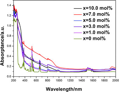 | ||
| Fig. 3 Absorption spectra of (Y0.95Er0.05)2O2S–xBi2O3 (x = 0, 1.0, 3.0, 5.0, 7.0, 10.0 mol%) samples. | ||
Also, in Y2O2S:Er3+ samples containing Bi2O3, we observed 1960 nm absorption band. This band does not exist in other Y2O2S:Er3+ samples without containing Bi2O3. This phenomenon is very interesting, which needs to be further researched. From Fig. 3, we can deduce that a small part of Bi ions may be doped into the Y2O2S host.
Excited by a 1550 nm laser at a power of 336 mW, room temperature UC luminescence spectra of the samples with different Bi2O3 concentrations are shown in Fig. 4. The inset shows a photograph of the UC emission in the sample (x = 10.0 mol%) under 1550 nm excitation. The emission spectra in the 520–700 nm range are characterized by an intense green band at 546 nm followed by a weaker red band at 671 nm. Although the addition of Bi2O3 lowered the luminescence intensity, most samples (x = 7.0 mol% or 10.0 mol%) still exhibited strong emission to the naked eyes, which insure such doped phosphors can still find wide spread applications in some special areas, which require good coating uniformity and resolving capability.
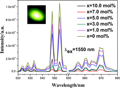 | ||
| Fig. 4 UC luminescence spectra of (Y0.95Er0.05)2O2S–xBi2O3 (x = 0, 1.0, 3.0, 5.0, 7.0, 10.0 mol%) samples excited by a 1550 nm laser (336 mW). The inset is the photograph of the UC emission of the sample (x = 10.0 mol%) excited by a 1550 nm laser (336 mW). | ||
The UC process in the Er3+ system is well understood and is briefly explained in the energy level diagram in several reports.23–30 For our case, the up-conversion mechanisms can be explained on the basis of various processes such as three photon absorption, excited state absorption and cross relaxation from energy transfer process. Emission bands observed at 671 nm, 546 nm, and 524 nm are assigned to the transitions 4F9/2→4I15/2, 4S3/2→4I15/2, 2H11/2→4I15/2 of Er3+, respectively. The emission intensity decreased with the doping of Bi. Furthermore, the relationship of luminescence intensity with the Bi dopant, is inversely related to the absorption intensity in VIS (green-red) region, which is due to the absorption of the Er3+ emission at the visible range by Bi ions. The decrease of UC luminescence intensity, in comparison with the Bi-free sample, can be explained by two reasons. On one hand, the emission intensity declines as grain size decreases. As reported in the literature,31 typically the larger the phosphor particle size, the higher the emission intensity. Well crystallized large phosphors have high luminous efficiency. Phosphors with a small particle size typically have strong scattering and low emission intensity. In addition, small phosphor particles typically contain more surface defects owing to incomplete crystallization, which can largely reduce the UC emission intensity. On the other hand, in samples containing Bi2O3, the Y2O2S host is doped with a small amount of Bi ions (shown in Fig. 3). The samples exhibit strong absorption in the VIS (green-red) region, and the emissions are absorbed by themselves. Even with strong absorption, the UC emissions of samples containing Bi2O3 are still sufficiently strong to the naked eyes excited by a 1550 nm laser (336 mW).
4. Conclusions
Herein we reported controlled growth of Y2O2S:Er3+ particles for the first time via high-temperature solid-state reaction, by addition of Bi2O3 in phosphor raw materials. The addition of Bi2O3 greatly influenced the grain growth of Y2O2S. The mechanisms relating to Y2O2S grain growth were rate controlling, depending on the amount of Bi2O3 liquid phase due to the low melting point of Bi2O3 (700 °C): (i) solution-re-precipitation process; (ii) diffusion of atoms through the Bi2O3-rich liquid phase. The UC luminescence properties were dependent on the microstructure and Bi2O3 concentrations. Optimum addition of Bi2O3 led to fine phosphor grains and high UC luminescence. The fine Y2O2S:Er3+ UC phosphors, which possess good coating uniformity and resolving capability, offers several potential applications such as color displays and biomedical imaging.
Acknowledgements
This work is financially supported by the Natural Science Foundation of Shanghai (11ZR1409300, 12ZR1407600) , the Fundamental Research Funds for the Central Universities (WD1014035), and the Shanghai Leading Academic Discipline Project (B502). L.S. would like to thank the U.S. Department of Agriculture (2011-38422-30803), the ACS Petroleum Research Fund, and Research Corporation for Science Advancement for partial support for this research.References
- J. W. Zhao, M. Dong, Y. G. Zhao and X. G. Kong, Adv. Mater. Res., 2012, 510, 609 CrossRef CAS
.
- J. H. Chung, J. H. Ryu, J. W. Eun, J. H. Lee, S. Y. Lee, T. H. Heo, B. G. Choi and K. B. Shim, J. Alloys Compd., 2012, 522, 30 CrossRef CAS
- X. D. Qi, C. M. Liu and C. C. Kuo, J. Alloys Compd., 2010, 492, L61 CrossRef CAS
- G. F. J. Garlick and C. L. Richards, J. Lumin., 1974, 9, 432 CrossRef CAS
- P. D. Han, L. Zhang, L. X. Wang and Q. T. Zhang, J. Rare Earths, 2011, 29, 849 CrossRef CAS
- G. A. Kumar, M. Pokhrel, A. Martinez, R. C. Dennis, I. L. Villegas and D. K. Sardar, J. Alloys Compd., 2012, 513, 559 CrossRef CAS
- L. Liu, Y. X. Wang, X. R. Zhang, K. Yang, J. Li, G. Liu and Y. L. Song, J. Lumin., 2012, 132, 1483 CrossRef CAS
- C. Y. Cao, X. M. Zhang, M. L. Chen, W. P. Qin and J. S. Zhang, J. Alloys Compd., 2010, 505, 6 CrossRef CAS
- G. S. Yi, H. C. Lu, S. Y. Zhao, Y. Ge, W. J. Yang, D. P. Chen and L. H. Guo, Nano Lett., 2004, 4, 2191 CrossRef CAS
- S. Altin, M. A. Aksan, E. Altin, Y. Balci and M. E. Yakinci, J. Supercond. Novel Magn., 2011, 24, 331 CrossRef CAS
- T. Ohkura, Y. Fujimoto, M. Nakatsuka and S. Young-Seok, J. Am. Ceram. Soc., 2007, 90, 3596 CrossRef CAS
- Y. F. Wei, C. H. Kao, C. F. Yang, H. H. Huang and C. J. Huang, Mater. Lett., 2007, 61, 4643 CrossRef CAS
- M. Drofenik, A. Znidarsic and D. Makovec, J. Am. Ceram. Soc., 1998, 81, 2841 CrossRef CAS
- S. Hingorani and D. O. Shah, J. Mater. Res., 1995, 10, 461 CrossRef CAS
- M. L. S. Teo, L. B. Kong, Z. W. Li and Y. B. Gan, J. Alloys Compd., 2008, 459, 557 CrossRef CAS
- K. Sun, Z. W. Lan, Z. Yu, L. Z. Li, J. M. Huang and X. N. Zhao, J. Phys. D: Appl. Phys., 2008, 41, 235002 CrossRef
- C. Wagner, Elektrochem., 1961, 65, 581 CAS
- E. P. Chukova, Moscow: Sovetskoe Radio, 1980 Search PubMed.
- C. H. An, S. T. Wang and Y. Q. Liu, Mater. Lett., 2007, 61, 2284 CrossRef CAS
- M. Y. Peng, J. R. Qiu, D. P. Chen, X. G. Meng and C. S. Zhu, Opt. Express, 2005, 13, 6892 CrossRef CAS
- T. Suzuki and Y. Ohishi, Appl. Phys. Lett., 2006, 88, 191912 CrossRef
- Y. Arai, T. Suzuki, Y. Ohishi, S. Morimoto and S. Khonthon, Appl. Phys. Lett., 2007, 90, 261110 CrossRef
- G. A. Kumar, M. Pokhrel and D. K. Sardar, Mater. Lett., 2012, 68, 395 CrossRef CAS
- J. Guo, F. Z. Ma, S. N. Gu, Y. Shi and J. J. Xie, J. Alloys Compd., 2012, 523, 161 CrossRef CAS
- M. Glauco, S. R. Nikifor, F. Michael, C. S. Isabel and C. P. B. Carlos, Appl. Phys. Lett., 2006, 89, 081109 CrossRef
- S. Ivanova and F. Pellé, J. Opt. Soc. Am. B, 2009, 26, 1930 CrossRef CAS
- G. Y. Chen, T. Y. Ohulchanskyy, A. Kachynski, H. Agren and P. N. Prasad, ACS Nano, 2011, 5, 4981 CrossRef CAS
- T. Trupke, A. Shalav, B. S. Richards, P. Würfel and M. A. Green, Sol. Energy Mater. Sol. Cells, 2006, 90, 3327 CrossRef CAS
- X. B. Chen, Opt. Commun., 2004, 242, 565 CrossRef CAS
- P. Xie and S. Rand, J. Opt. Soc. Am. B, 1994, 11, 901 CrossRef CAS
- Y. S. Chen, W. He, H. H. Wang, X. L. Hao, Y. C. Jiao, J. X. Lu and S. E. Yang, J. Lumin., 2012, 132, 2404 CrossRef CAS
| This journal is © The Royal Society of Chemistry 2012 |