Comparison between metal ion and polyelectrolyte functionalization for electrophoretic deposition of graphene nanosheet films†
Juan
Yang
ab,
Xingbin
Yan
*ab,
Jiangtao
Chen
ab,
Haibin
Ma
c,
Dongfei
Sun
ab and
Qunji
Xue
b
aLaboratory of Clean Energy Chemistry and Materials, Lanzhou Institute of Chemical Physics, Chinese Academy of Science, Lanzhou, 730000, P. R. China. E-mail: xbyan@licp.cas.cn; Fax: +86 931 4968055; Tel: +86 931 4968055
bState Key Laboratory of Solid Lubrication, Lanzhou Institute of Chemical Physics, Chinese Academy of Sciences, Lanzhou, 730000, P. R. China
cGansu province Hospital of traditional Chinese medicine, Lanzhou, 730050, P. R. China
First published on 15th August 2012
Abstract
Graphene nanosheets (GNSs) were modified either by metal magnesium (Mg) ions or a polyelectrolyte, polydiallyldimethylammonium chloride (PDDA), to produce positive charges on them. The two materials were used to produce GNS films with different surface morphologies. They were deposited on single-crystal silicon substrates using simple direct current electrophoretic deposition method. The Mg ion-modified GNS film has a relatively rough surface with some GNSs almost perpendicular to the surface, whereas the PDDA-modified GNS film has a relatively smooth surface with most GNSs parallel to the substrate. This difference is attributed to the different interactions of Mg ions and PDDA molecules with GNSs. Because of the favorable surface morphology, the Mg ion-modified GNS film displays better field emission compared with the PDDA-modified GNS film. Biocompatibility tests indicate that the rougher Mg ion-modified GNS film is more beneficial to cell adhesion and growth.
1. Introduction
Graphene as a single layer of carbon atoms has triggered exciting research in material science, and it shares many similar or even identical properties with other nano-scale carbon allotropes. Owing to its excellent electronic transport properties, extremely high mechanical stiffness, exceptional thermal, electrical conductivity, atomic thickness, and high aspect ratio, graphene has been predicted to hold great promise for many potential applications in nanoelectronics, batteries, reinforced materials, supercapacitors, and field emitters.1–5 Up to now, many approaches, such as micromechanical cleavage of highly oriented pyrolytic graphite, sublimation of silicon from silicon carbide, chemical vapor deposition, arc discharge, solid-state dissolution, solar radiation and chemical conversion in liquid-phase, have been developed to prepare graphene.6–10 Considering the bulk production and the practical applications, the chemical conversion of graphite in liquid-phase has been considered as the most effective method. Therefore, in this paper, chemical conversion in the liquid-phase has been used.11–15 This method involves the chemical oxidation of graphite, the exfoliation of graphite oxide (GO) and the subsequent chemical reduction.16,17Electrophoretic deposition (EPD) is an economical and versatile processing technique to prepare various coatings. As recently demonstrated by Cheng and co-workers, macroscopic graphene films can be prepared by EPD.18 Due to EPD’s many advantages, such as high deposition rate, low cost combined with the simplicity of preparation, solvent-based manufacturing, and the use of wide range of substrates, graphene films prepared by EPD have much potential for electrical batteries, supercapacitors, and field emission displays.19–24
Generally, EPD includes two key steps. First, charged colloidal particles in a liquid-phase suspension are forced to move toward the oppositely charged electrode under an electric field. Second, these charged particles are coherently deposited onto the surface of the electrode. As the surface charges of a graphene nanosheet (GNS) are ignorable,12 GNSs cannot move to an oppositely charged electrode or deposit on it under an electric field. Thus, in order to prepare a GNS film by EPD, GNSs have to be given charges and a stable suspension of charged GNSs needs to be obtained in advance.
As we know, the hexagon ring arrangements of sp2-bonded carbon atoms form into the geometrically planar surfaces of GNSs. Also, for chemically-reduced GNSs, there are some residual carboxyl groups existing on the edges of the GNSs.12 Therefore, if different modification methods are used to produce charges on the planar surfaces of GNSs or at the edges of GNSs, it is highly probable that it will be possible realize the controllable preparation of GNS films with different morphologies by EPD.
In this study, GNSs were modified either by magnesium nitrate (Mg(NO3)2·6H2O) or a common polyelectrolyte polydiallyldimethylammonium chloride (PDDA). Due to the different decoration mechanisms of Mg ions and PDDA molecules with GNSs, two kinds of GNS films with different surface morphologies were deposited on silicon substrates using simple direct current (DC) EPD. Furthermore, the difference in the surface morphology resulted in different performances in the field emission and the biocompatibility.
2. Experimental
2.1. Materials
Graphite powder (325 mesh) was purchased from Qingdao Huatai Tech. Co., Ltd. 20 wt% PDDA (MW = 200![[thin space (1/6-em)]](https://www.rsc.org/images/entities/char_2009.gif) 000–350000 g mol−1) aqueous solution was purchased from Aldrich. Mg(NO3)2·6H2O, isopropyl alcohol and anhydrous methanol were purchased from Tianjin Chemical Reagent Co., Ltd. Fetal bovine serum (FBS) was purchased from Hangzhou Sijiqing Bio. Engineer. Mater. Co., Ltd., China. MC3T3-E1 cells and RPMI 1640 medium were purchased from Lanzhou Shenggong Biomedical Co., Ltd., China. Dulbecco's modified Eagle's medium (DMEM) was purchased from Gibco. Trypsin-EDTA solution and 3-(4, 5-dimethylthiazol-2-yl)-2, 5-diphenyltetrazolium bromide were purchased from Sigma. Other reagents were commercially available and were of analytical reagent grade. Twice-distilled water with a resistance about 18.0 MΩ cm−1 was used throughout. N-type Si (111) wafers with a sheet resistance of 0.01–0.02 Ω cm−2 were used as the substrates for depositing GNS films.
000–350000 g mol−1) aqueous solution was purchased from Aldrich. Mg(NO3)2·6H2O, isopropyl alcohol and anhydrous methanol were purchased from Tianjin Chemical Reagent Co., Ltd. Fetal bovine serum (FBS) was purchased from Hangzhou Sijiqing Bio. Engineer. Mater. Co., Ltd., China. MC3T3-E1 cells and RPMI 1640 medium were purchased from Lanzhou Shenggong Biomedical Co., Ltd., China. Dulbecco's modified Eagle's medium (DMEM) was purchased from Gibco. Trypsin-EDTA solution and 3-(4, 5-dimethylthiazol-2-yl)-2, 5-diphenyltetrazolium bromide were purchased from Sigma. Other reagents were commercially available and were of analytical reagent grade. Twice-distilled water with a resistance about 18.0 MΩ cm−1 was used throughout. N-type Si (111) wafers with a sheet resistance of 0.01–0.02 Ω cm−2 were used as the substrates for depositing GNS films.
2.2 Preparation of GNSs by reduction of graphene oxide (GO)
GO was prepared from the natural graphite by following the methodology reported by Shi et al.7 After that, GO was reduced by hydrazine solution with ammonia water.242.3 Modification of GNSs with Mg ions and EPD of GNS film
6 mg of GNS powders and 6 mg of Mg(NO3)2 were dispersed into 120 mL of anhydrous isopropyl alcohol with the aid of sonication using a high-power (800 W) ultrasonic probe at 0 °C for 30 min. A homogeneous suspension of the Mg-modified GNS (0.05 mg mL−1) was obtained, and it was used as the electrolyte. A simple electrolytic cell system was used to deposit a GNS film.25 A high-purity platinum plate (99.99%, 35 mm × 20 mm) was mounted on the positive graphite electrode. A silicon wafer was mounted on the negative graphite electrode and kept 10 mm away from the counter electrode. For every electrodeposition experiment, a Si substrate was first immersed in an aqueous solution of 5% HF for a few minutes to remove the native oxide layer, sequentially cleaned in an ultrasonic bath with H2O, ethanol, and acetone, and then placed into the electrolyte, with an area of 15 mm × 10 mm to be immersed therein. The EPD was carried out at an applied DC voltage of 300 V, a constant temperature of 50 °C and a deposition duration of 3 min, to form an Mg-modified GNS film.2.4 Modification of GNSs with PDDA and EPD of GNS film
6 mg of GNS powders was dispersed into a 30 mL of 1 wt% PDDA aqueous solution with the aid of sonication at the same condition. The resulting suspension was centrifuged at 16000 rpm for 20 min to precipitate all of the PDDA-modified GNSs on the bottom of the centrifugal tubes. After removing the upper PPDA aqueous solution, the precipitate was repeatedly washed with H2O to remove excess PDDA molecules and then repeatedly washed with anhydrous methanol to remove H2O molecules. After that, a homogeneous methanol suspension of the PDDA-modified GNS (0.05 mg mL−1) was obtained. Subsequently, the electrodeposition was carried out with the same parameters for depositing Mg-modified GNS film except the deposition duration was 10 min (in order to obtain nearly identical thickness), to form a PDDA-modified GNS film.
2.5 Characterizations
The morphology and microstructure of powdery GNSs and films were characterized by a field-emission scanning electron microscope (FESEM, JSM-6701F), X-ray diffraction (XRD, Philips X′Pert Pro.) using Cu-Kα radiation and a Fourier transformation infrared spectrometer (FTIR, a Bruker IFS66V). The composition of the GNS films were examined by an energy-dispersive spectrometer (EDS) equipped on SEM (JSM-5600LV). Raman spectra were recorded using a micro-Raman spectroscopy (JY-HR800, the excitation wavelength of 532 nm). The ζ potentials of different GNS suspensions were measured using a Zetasizer Nano Instrument (Nano-ZS, United Kingdom Malvern Instruments Ltd.), and final data were obtained by averaging three measurements for each sample.2.6 Field emission measurements
The GNS films were placed in a muffle furnace and calcined at 200 °C in Ar for 3 h with a heating rate of 2 °C min−1 to enhance cohesion between GNSs and substrates.The field emission characteristics of the GNS films were estimated in a vacuum chamber under base pressure 10−6 Pa at room temperature using a computer-controlled power source with an amperometer (Keithley 248). A stainless-steel plate was used as the anode and the silicon substrate coated with GNS film was served as the cathode. The emission area was 0.5 cm2. The distance between the cathode and the anode was kept 300 μm, which was adjusted with a spiral micrometer before the measurements. The electron emission turn-on field in the experiment is defined as the electric field (F) for a current density (J) of 10 μA cm−2 and the threshold field is 100 μA cm−2. The data were collected automatically by the computer.
2.7 Biocompatibility test
Before the biocompatibility tests, the film samples were cut into quadrate pieces of approximately 10 mm × 10 mm, soaked in 75% ethanol for 1 h to sterilize, and exchanged with PBS for three times (30 min each). The cut samples were then washed with RPMI-1640 containing 10% FBS for two times (2 h each). After that, quantitative cells (2 × 10⁵ cells well−1) were seeded on each sample surface, allowing them to incubate for 48 h.
For SEM observation, after being cultured for 48 h, the cells attached on each sample were washed with PBS (pH = 7.4), fixed by 2.5 wt% glutaraldehyde in PBS at 4 °C for 2 h, rinsed with PBS, fixed again by 1 wt% osmium tetroxide in PBS at 4 °C for 1 h. After that, standard dehydration in an ethanol graded series (50%, 70%, 95%, and 100%) and critical point drying were performed. Finally, the samples were coated with gold in a vacuum for the investigation of SEM.
3. Results and discussion
FESEM and XRD were used to analyze the morphology and structure of as-obtained powdery GNSs reduced by hydrazine hydrate.As Fig. 1a shows, the GNSs are nearly transparent, suggesting that the GNSs are quite thin. The observed wrinkles were probably caused by the oxygen functionalization and the resultant defects during the preparation of GO.26 As shown in Fig. 1b, the XRD pattern of graphite shows an intense (002) diffraction peak at 26.5°, corresponding to a c-axis spacing of 0.34 nm. The XRD pattern of GO shows a strong (002) diffraction peak at 12.1°, corresponding to a c-axis spacing of 0.73 nm. However, after chemical reduction, a broad (002) diffraction peak at 24° appears, corresponding to a c-axis spacing of 0.36 nm. This value is consistent with that of chemically reduced GO powders in previous reports.24
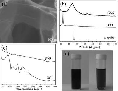 | ||
| Fig. 1 (a) FESEM image of the GNSs; (b) XRD patterns of powdery graphite, GO and GNS samples; (c) FTIR spectra of powdery GO and GNS samples; (d) photographs of Mg- and PDDA-modified GNSs dispersed in isopropyl and methanol, respectively. | ||
To verify the chemical composition of GO and graphene, the infrared spectra of the products were investigated, as shown in Fig. 1c. For the GO, the characteristic vibrations include the broad and intense O–H peak at 3400 cm−1, strong C![[double bond, length as m-dash]](https://www.rsc.org/images/entities/char_e001.gif) O peak in carboxylic acid and carbonyl moieties at 1732 cm−1, C–OH peak at 1365 cm−1, C–O–C peak at 1246 cm−1, C–O stretching peak at 1065 cm−1, and aromatic C–H peak at 832 cm−1.27 The peak centered at 1590–1620 cm−1 is assigned to adsorbed water molecules, but may be also containing components from skeletal vibrations of unoxidized graphitic domains.16 For the GNSs, the obvious broad peak at 3200–3600 cm−1 is attributed to N–H and O–H bonds, the peaks between 1100 and 1650 cm−1 are associated with the stretching vibrations of both double and single C–N and C–C bonds, and the stretching of C–H bonds. Since the overlapping of the strong adsorption of graphene sheets in this region, the precise classification is not feasible as that for GO.
O peak in carboxylic acid and carbonyl moieties at 1732 cm−1, C–OH peak at 1365 cm−1, C–O–C peak at 1246 cm−1, C–O stretching peak at 1065 cm−1, and aromatic C–H peak at 832 cm−1.27 The peak centered at 1590–1620 cm−1 is assigned to adsorbed water molecules, but may be also containing components from skeletal vibrations of unoxidized graphitic domains.16 For the GNSs, the obvious broad peak at 3200–3600 cm−1 is attributed to N–H and O–H bonds, the peaks between 1100 and 1650 cm−1 are associated with the stretching vibrations of both double and single C–N and C–C bonds, and the stretching of C–H bonds. Since the overlapping of the strong adsorption of graphene sheets in this region, the precise classification is not feasible as that for GO.
In this study, magnesium nitrate and PDDA were used to modify GNSs. Fig. 1d shows a stable isopropyl alcohol suspension of the Mg-modified GNSs (0.05 mg mL−1) and a stable methanol suspension of the PDDA-modified GNSs (0.05 mg mL−1). Although the stable GNS suspension can be obtained by either Mg ion or PDDA modification, the two mechanisms are distinctly different. For PDDA modification, PDDA is a water-soluble quaternary ammonium and strong polyelectrolyte, which leads to a high functionalization or/and coverage of PDDA chains on GNSs.28,29 PDDA has a hydrophobic backbone, which can interact with the GNS through hydrophobic Van der Waals interactions. Furthermore, the ζ potential of the pristine GNSs is negative (−11.4 mV, dispersed in methanol), which is ascribed to some residual carboxyl groups on the edges of GNSs. In comparison, the ζ potential of the PDDA-modified GNSs is positive (20.6 mV, dispersed in methanol), because of the coverage of polymeric cationic PDDA molecules on GNSs. The edges of chemically reduced GO sheets retain many oxygen-containing groups such as hydroxyl and epoxide (as shown in Fig. 1c). For Mg ion modification, Mg ions were adsorbed on the edges of GNSs by electrostatic interaction. However, the precise value of the ζ potential could not be obtained as the potential of the isopropyl alcohol suspension of Mg-modified GNSs was not stable during the measurement.
As shown in Fig. 2, it is revealed that the morphologies of the Mg-modified GNS film and the PDDA-modified GNS film are distinct different. The former forms a porous structure, resulting in the film surface being relatively rough (Fig. 2a and 2c). Also, the EDS analysis result shows that there is a signal peak attributed to Mg element, indicating the existence of Mg in the resulting GNS film. On the contrary, the later is compact and the surface is relatively smooth with most GNSs lying flat on the substrate (Fig. 2d and 2f). As seen from the cross-section views, the Mg ion-modified GNS film has a relatively rough surface with some GNSs nearly vertical on the substrate, whereas the PDDA-modified GNS film has a relatively smooth surface with most GNSs lying flat on the substrate.
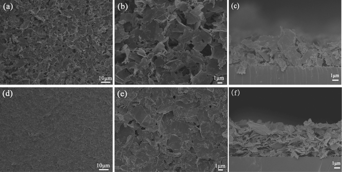 | ||
| Fig. 2 SEM images of two kinds of GNS films deposited from: (a–c) the isopropyl alcohol suspension of the Mg-modified GNSs, and (e, f) the methanol suspension of the PDDA-modified GNSs. | ||
According to the different modification mechanisms and surface morphologies, the schematic diagrams of EPD for the two kinds of GNS films are shown in Fig. 3. Because the edges of the GNSs have adsorbed Mg2+ ions and take some positive charges, these positively charged edges would preferentially migrate toward the negative electrode and be adsorbed onto the surface of the Si substrate under the electric field. Along with the EPD process, the GNSs are randomly oriented and some of them are almost perpendicular to the substrate, forming a loose and porous GNS film. In addition, during the EPD process, Mg(NO3)2 can be electrochemically reduced and also deposited as Mg(OH)2 on the Si substrate which is the support for the GNSs, according to the following reactions:30
| NO−3 + 2H2O + 2e− = NO−2 + 2OH− |
| 2H2O + 2e− = 2OH− + H2 |
| Mg2+ + 2OH− = Mg(OH)2 |
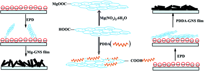 | ||
| Fig. 3 Scheme of the deposition mechanism of two kinds of GNS films. | ||
In comparison, because the basal planes of GNSs are decorated by the positively charged PDDA molecules by π–π interactions, these positively charged plane surfaces would preferentially migrate and be adsorbed onto the surface of the Si substrate under the electric field, and as a result almost all the GNSs lie flat on the substrate to form a relatively smooth surface.
Raman spectra were employed to investigate these GNS films. As shown in Fig. 4, all of Raman spectra of the samples show two prominent peaks, which are indexed to the D and G peaks. The D peak became broader for GO, which is due to inter-valley scattering. The G peak of GO locates at higher frequency than that of graphite, which due to the high oxygen content after chemical oxidation.16 After reduced, the G peak of GNS shifts to low frequency, confirming the restoration of the graphitic sp2 network in graphene during the reduction. Inevitably, the graphene retains some oxygen groups of hydroxyl and carboxyl after reduction, which led to a blue shift of the G peak from 1580 cm−1 to 1605 cm−1. Moreover, the peak at 2700 cm−1 (2D peak) is also found. The positions of the D, G and 2D peaks, the intensity ratio of the G peak to D peak, the full-width at half-maximum of the 2D peak and the ratio of the G peak to the 2D peak are all identical. Moreover, XPS investigations were also conducted. The C1s spectra of Mg- and PDDA modified GNS films show no remarkable difference, which indicates that the two GNS films have no obvious change in the microstructure (the XPS spectra can be found in ESI† for details).
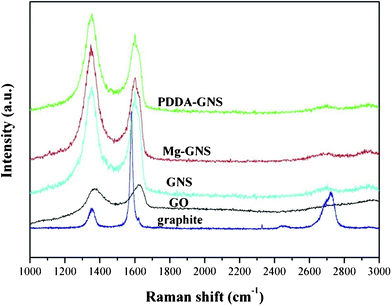 | ||
| Fig. 4 Raman spectra of the two kinds of GNS films. | ||
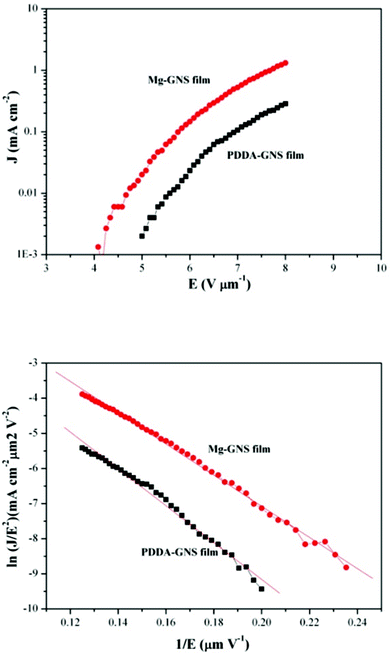
One of the potential applications of GNSs is in field electron emission source. To date, much work, including theoretical calculation and experimental investigations, has been devoted to study the FE from GNSs.31–33 It has been demonstrated that graphene is an ideal material for FE, which shows promising electron-emission properties, such as low turn-on electrical field, large emission current density and good emission stability. The typical emission-current density as a function of the applied electric field (J–E curves) of the Mg-modified and the PDDA-modified GNS films are shown in Fig. 5a. According to the J–E curves, the turn-on electric field (Eto) and threshold field (Ethr) can be obtained. For the Mg-modified GNS film, Eto is 4.67 V μm−1 and Ethr is 5.78 V μm−1. For the PDDA-modified GNSs film, Eto is 5.57 V μm−1 and Ethr is 7.00 V μm−1.
 | ||
| Fig. 5 Field emission characteristics of two kinds of GNS films: (a) J–E plots; (b) F–N plots. | ||
Therefore, the Mg-modified GNS film displays better FE behaviours. The difference in the FE performance is mainly attributed to the different surface morphologies. As shown in Fig. 2c, some Mg-modified GNSs are deposited vertically on the substrate. These vertically oriented GNSs would play an obvious role in enhancing the FE. Of course, it should be mentioned that metal ions might also affect the FE behavior of GNSs. Modification with different ions will change the work function of graphene, as a result of the change of FE of graphene.34,35
The corresponding Fowler–Nordheim (F–N) plots are displayed in Fig. 5b. The linear behavior indicates that the emission current is indeed the result of cold cathode FE and the emission current from the GNS films obeys the conventional FN equation, which is derived from the electron emission through the surface potential barrier under the intense applied field:36,37
| J = A(E)2exp(−Bϕ3/2β−1E−1) |
The value of β may be attributed to the statistical variation of geometrical, structural, and electronic characteristics of field emitting sites. According to our early reports,20,21 we assume that ϕ is 5 eV. Based on the equation above, β can be obtained from the linear region of the FN plot. The values of β for the Mg-modified GNS film and the PDDA-modified GNS film were determined to be ∼1720 and ∼1455, respectively. The higher enhancement factor β for the Mg-modified GNS film was attributed to the morphology of the graphene nanosheets perpendicular to the Si substrate, leading to the lower Eto and higher current density, which can be found in the J–E curve shown in Fig. 5.
Recently, GNSs have been proved to exhibit excellent biocompatibility and highly antibacterial activity.38,39 To study the cytocompatibilities of the two film samples, MC3T3-E1 cells were used in our system, which is commonly used to assess cytotoxicity of potential substrates for cell growth. Fig. 6 shows the cell proliferation results. It is clear seen that the number of the survived cells on the Mg-modified GNS film is more than that on the PDDA-modified GNS film. Also, as SEM images show, after the cell growth, the cells attach firmly on the Mg-modified GNS film and exhibit a favorable growth status. It indicates that the Mg-modified GNS film promotes cell seeding as well as the cells secreted extracellular matrix (ECM), which shows better biocompatibility.
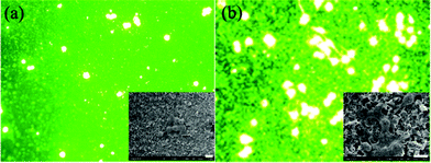 | ||
| Fig. 6 Fluorescent microscopy images of MC3T3-E1 cells grown on the PDDA-GNS film (a) and on the Mg-GNS film (b) for 48 h. The magnification is ×100 for each image. Insets are the SEM images of grown MC3T3 E1 cells. The scale is 10 μm. | ||
The biomaterial interface plays an active regulating role in controlling the cell attachment and morphology.40 Nanostructured surfaces have the capability of enhancing osteoblastic proliferation and differentiation.41,42 In our system, the Mg-modified GNS film displays a porous and a rougher surface compared with the PDDA-modified GNS film, which is favorable to the adhesion, proliferation and growth of cells on it.
4. Conclusion
The effect of Mg ion and PDDA functionalization of GNSs on the subsequent electrophoretically deposited GNS films was carried out. Due to the different interactions of Mg ions and PDDA molecules with GNSs, the resulting GNS films display two kinds of distinct surface morphologies. Especially, the Mg ion-modified GNS film exhibits a relatively rough and porous surface, resulting in better field emission and biocompatibility compared with the PDDA-modified GNS film.Acknowledgements
The authors acknowledge the support from the Top Hundred Talents Program of Chinese Academy of Sciences and the National Nature Science Foundation of China (51005225 and 51002161).References
- M. Freitag, Nat. Nanotechnol., 2008, 3, 455–457 CrossRef CAS.
- E. J. Yoo, J. Kim, E. Hosono, H. S. Zhou, T. Kudo and I. Honma, Nano Lett., 2008, 8, 2277–2282 CrossRef CAS.
- S. Stankovich, D. A. Dikin, G. H. B. Dommett, K. M. Kohlhaas, E. J. Zimney, E. A. Stach, R. D. Piner, S. T. Nguyen and R. S. Ruoff, Nature, 2006, 442, 282–286 CrossRef CAS.
- Q. Wu, Y. X. Xu, Z. Y. Yao, A. R. Liu and G. Q. Shi, ACS Nano, 2010, 4, 1963–1970 CrossRef CAS.
- G. Eda, U. H. Emrah, N. Rupesinghe, G. A. J. Amaratunga and M. Chhowalla, Appl. Phys. Lett., 2008, 93, 233502–233502-3 CrossRef.
- C. Berger, Z. Song, X. Li, X. Wu, N. Brown, C. Naud, D. Mayou, T. Li, J. Hass and A. N. Marchenkov, Science, 2006, 312, 1191 CrossRef CAS.
- Y. Xu, H. Bai, G. Lu, C. Li and G. Shi, J. Am. Chem. Soc., 2008, 130, 5856–5857 CrossRef CAS.
- G. Nandamuri, S. Roumimov and R. Solanki, Nanotechnology, 2010, 21, 145604 CrossRef CAS.
- Y. Wu, B. Wang, Y. Ma, Y. Huang, N. Li, F. Zhang and Y. Chen, Nano Res., 2010, 3, 661–669 CrossRef CAS.
- S. Sasikaladevi, J. Aravind, V. Eswaraiah and S. Ramaprabhu, J. Mater. Chem., 2011, 21, 17094–17097 RSC.
- Y. Liang, D. Wu, X. Feng and K. Müllen, Adv. Mater., 2009, 21, 1679–1683 CrossRef CAS.
- D. Li, M. B. Muller, S. Gilje, R. B. Kaner and G. G. Wallace, Nat. Nanotechnol., 2008, 3, 101–105 CrossRef CAS.
- X. Fan, W. Peng, Y. Li, X. Li, S. Wang, G. Zhang and F. Zhang, Adv. Mater., 2008, 20, 4490–4493 CrossRef CAS.
- C. Nethravathi and M. Rajamathi, Carbon, 2008, 46, 1994–1998 CrossRef CAS.
- G. Williams, B. Seger and P. V. Kamat, ACS Nano, 2008, 2, 1487–1491 CrossRef CAS.
- S. Stankovich, D. A. Dikin, R. D. Piner, K. A. Kohlhaas, A. Kleinhammes, Y. Jia, Y. Wu, S. B. T. Nguyen and R. S. Ruoff, Carbon, 2007, 45, 1558–1565 CrossRef CAS.
- H. C. Schniepp, J. L. Li, M. J. McAllister, H. Sai, M. Herrera-Alonso, D. H. Adamson, R. K. Prud'homme, R. Car, D. A. Saville and I. A. Aksay, J. Phys. Chem. B, 2006, 110, 8535–8539 CrossRef CAS.
- Z. S. Wu, S. Pei, W. Ren, D. Tang, L. Gao, B. Liu, F. Li, C. Liu and H. M. Cheng, Adv. Mater., 2009, 21, 1756–1760 CrossRef CAS.
- J. Ding, X. B. Yan, J. Li, B. S. Shen, J. Yang, J. T. Chen and Q. J. Xue, ACS Appl. Mater. Interfaces, 2011, 3, 4299–4305 CAS.
- J. Li, J. T. Chen, B. S. Shen, X. B. Yan and Q. J. Xue, Appl. Phys. Lett., 2011, 99, 163103 CrossRef.
- J. T. Chen, J. Li, J. Yang, X. B. Yan, B. K. Tay and Q. J. Xue, Appl. Phys. Lett., 2011, 99, 173104 CrossRef.
- Y. Chen, X. Zhang, P. Yu and Y. W. Ma, J. Power Sources, 2010, 195, 3031–3035 CrossRef CAS.
- S. J. Wang, Y. Geng, Q. B. Zheng and J. K. Kim, Carbon, 2010, 48, 1815–1823 CrossRef CAS.
- X. B. Yan, J. T. Chen, J. Yang, Q. J. Xue and P. Miele, ACS Appl. Mater. Interfaces, 2010, 2, 2521–2529 CAS.
- J. Yang, J. T. Chen, S. X. Yu, X. B. Yan and Q. J. Xue, Carbon, 2010, 48, 2665–2668 CrossRef CAS.
- T. Ramanathan, A. A. Abdala, S. Stankovich, D. A. Dikin, M. Herrera Alonso, R. D. Piner, D. H. Adamson, H. C. Schniepp, X. Chen, R. S. Ruoff, S. T. Nguyen, I. A. Aksay, R. K. Prud'Homme and L. C.Brinson, Nat. Nanotechnol., 2008, 3, 327–331 CrossRef CAS.
- Y. Si and E. T. Samulski, Nano Lett., 2008, 8, 1679–1682 CrossRef CAS.
- S. Y. Wang, D. S. Yu, L. M. Dai, D. W. Chang and J. B. Baek, ACS Nano, 2011, 5, 6202–6209 CrossRef CAS.
- Y. X. Fang, S. J. Guo, C. Z. Zhu, Y. M. Zhai and E. K. Wang, Langmuir, 2010, 26, 11277–11282 CrossRef CAS.
- S. Santhanagopalan, F. Teng and D. D. Meng, Langmuir, 2011, 27, 561–569 CrossRef CAS.
- J. A. Driscoll, B. Cook, S. Bubin and K. Varga, J. Appl. Phys., 2011, 110, 024304 CrossRef.
- S. Sun, L. K. Ang, D. Shiffler and J. W. Luginsland, Appl. Phys. Lett., 2011, 99, 013112 CrossRef.
- H. Yamaguchi, K. Murakami, G. Eda, T. Fujita, P. F. Guan, W. C. Wang, C. Gong, J. L. Boisse, S. Miller, M. Acik, K. Cho, Y. J. Chabal, M. W. Chen, F. Wakaya, M. Takai and M. Chhowalla, ACS Nano, 2011, 5, 4945–4952 CrossRef CAS.
- U. A. Palnitkar, R. V. Kashid, M. A. More, D. S. Joag, L. S. Panchakarla and C. N. R. Rao, Appl. Phys. Lett., 2010, 97, 063102 CrossRef.
- L. S. Panchakarla, K. S. Subrahmanyam, S. K. Saha, A. Govindaraj, H. R. Krishnamurthy, U. V. Waghmare and C. N. R. Rao, Adv. Mater., 2009, 21, 4726–4730 CAS.
- X. B. Yan, T. Xu, S. Xu, H. Liu and S. R. Yang, Solid State Commun., 2005, 133, 113–116 CrossRef CAS.
- B. Satyanarayana, A. Hart, W. Milne and J. Robertson, Appl. Phys. Lett., 1997, 71, 1430 CrossRef CAS.
- W. B. Hu, C. Peng, W. J. Luo, M. Lv, X. M. Li, D. Li, Q. Huang and C. H. Fan, ACS Nano, 2010, 4, 4317–4323 CrossRef CAS.
- O. Akhavan and E. Ghaderi, ACS Nano, 2010, 4, 5731–5736 CrossRef CAS.
- M. A. Correa-Duarte, N. Wagner, J. Rojas-Chapana, C. Morsczeck, M. Thie and M. Giersig, Nano Lett., 2004, 4, 2233–2236 CrossRef CAS.
- R. L. Price, M. C. Waid, K. M. Haberstroh and T. J. Webster, Biomaterials, 2003, 24, 1877–1887 CrossRef CAS.
- T. J. Webster, C. Ergun, R. H. Doremus, R. W. Siegel and R. Bizios, Biomaterials, 2000, 21, 1803–1810 CrossRef CAS.
Footnote |
| † Electronic Supplementary Information (ESI) available. See DOI: 10.1039/c2ra20948a |
| This journal is © The Royal Society of Chemistry 2012 |