Standing pillar arrays of C-coated hollow SnO2 mesoscale tubules for a highly stable lithium ion storage electrode†
Jong
Guk Kim
ab,
Sang
Ho Lee
a,
Sang
Hoon Nam
ab,
Sung
Mook Choi
a and
Won
Bae Kim
*ab
aSchool of Materials Science and Engineering, Gwangju Institute of Science and Technology (GIST), Gwangju, 500-712, South Korea. E-mail: wbkim@gist.ac.kr; Fax: +82 62 7152304; Tel: +82 62 7152317
bResearch Institute for Solar and Sustainable Energies (RISE), Gwangju Institute of Science and Technology (GIST), Gwangju, 500-712, South Korea
First published on 21st June 2012
Abstract
This work reports the direct growth of hollow one-dimensional nanostructure arrays on conducting substrates for use as efficient electrodes in Li-ion batteries. The C-coated hollow SnO2 pillar array structures can be prepared by template-directed synthesis, selective wet etching, and a carbonization route. The well-oriented ZnO nanorod arrays, which are grown on titanium substrates, are used as a sacrificial template for the deposition of SnO2 layers through a simple hydrothermal process. The ZnO portions are selectively removed by wet etching, producing hollow SnO2 arrays that are consecutively covered with carbon layers via the carbonization of glucose. The lithium storage performance of the synthesized C-coated hollow SnO2 pillar array structures is demonstrated by applying them directly to a working electrode without additive materials. The standing pillar array electrode, consisting of C-coated hollow SnO2, exhibits an excellent discharge capacity of ca. 1251.9 mA h g−1 on the first cycle, and it also shows promising cyclability, rate capability, and coulombic efficiency, indicating that C-coated hollow SnO2 arrays fabricated on the current collector can be powerful candidates for a highly stable lithium storage electrode platform.
Introduction
Various metal oxides have been widely exploited as the anode materials in Li-ion batteries (LIBs) because of their high theoretical capacity, safety, abundance and relatively low cost.1–5 Among these, SnO2 has been regarded as a possible substitute for the conventional graphite anode due to its high theoretical specific capacity (ca. 781 mA h g−1), low cost, low toxicity and safety.6–9 However, the practical implementation of SnO2 is limited due to its large volume expansion (up to 300%), which leads to cracking and pulverization of the electrode during repeated charge/discharge cycles.10 To circumvent this problem, several approaches have been proposed for the creation of a highly stable SnO2-based electrode structure. For example, one-dimensional (1D) SnO2 nanotubes11–14 have gained significant interest as alternative electrode materials for long-term cyclability. Because the tubular structure itself has a high surface area, compared with other 1D structures,15–17 it can ameliorate the induced mechanical stress more efficiently during repetitive cyclings.18 In addition, surface modification on the SnO2 with a second phase such as carbon,19–21 Au,22 V2O523 and polypyrrole24 has attracted considerable attention for the development of a highly durable electrode. Among these, carbon has become the preferred surface coating material because carbonaceous materials have high electrical conductivity, good mechanical durability, and high reversible cycling features.9,19,20 Therefore, carbon-coated 1D SnO2 may provide significant advantages for the development of a highly stable lithium storage electrode.Thus far, nanostructured electrodes have been regarded as a promising solution to the limitations of current LIB technology. Unfortunately, there are also drawbacks in the traditional preparation methods for battery electrodes. For instance, some ancillary materials, including conductive agents and non-conductive polymeric binders, can lower the energy density of the electrode.25 Additionally, homogeneous dispersion of these materials is an issue in randomly mixed electrode films because of their agglomeration features.26 Furthermore, aggregation between electroactive nanomaterials often occurs as the charge/discharge cycles progress, causing limitations in the use of nanostructured materials as electrodes in LIBs.9 Therefore, if carbon-decorated hollow SnO2 pillar arrays are prepared directly on the current collector, this standing pillar array electrode could improve the cycling stability with following features: (i) an internal hollow cavity and intervals formed between neighboring pillars could accommodate mechanical stress efficiently during cycling and thus relieve rapid electrode degradation;26–31 (ii) directly grown hollow pillar arrays could reduce the nanoparticle agglomeration or pulverization that enables a decrease in the loss of electrical contact;29,30–34 and (iii) outer shell carbon layers could enhance the electronic conductivity and decrease the side reactions with the electrolyte that cause irreversible cycling and poor cycle life.35 Furthermore, electrons can be transferred from reaction sites to the current collector more effectively in these electrodes compared with electrodes containing non-standing materials.18 Consequently, these characteristics could significantly benefit LIBs fashioned from 1D tubular arrays and operated at a relatively high current density.
Here, we report the fabrication of C-coated hollow SnO2 pillar arrays directly onto a titanium current collector substrate, which is prepared through a template-directed synthesis method followed by selective wet etching and a carbonization process. The synthesized C-coated hollow SnO2 array electrode shows an excellent initial discharge capacity (1251.9 mA h g−1), long-term cycling stability, and high coulombic efficiency because this C-coated hollow SnO2 array platform fulfills the important requirements for LIB electrodes such as decent adhesion to the substrate, uniform coverage of the electroactive materials, large active sites, and high electrical conductivity.34 Furthermore, the energy density of this configuration is increased due to the fact that no auxiliary material is required, as compared to conventional electrodes.26,31 The morphology and dimensions of the C-coated SnO2 arrays are tunable by altering the dimensions of the sacrificial ZnO templates.
Experimental section
Growth of the ZnO nanorod arrays
ZnO nanorod arrays were prepared using a simple hydrothermal process that was slightly modified from previously reported methods.36 Titanium (Ti) substrates (thickness = 0.127 mm, 99.7%, Aldrich) were cleaned in ultrasonic baths that contained absolute acetone and ethanol, consecutively, and dried in a convection oven at 70 °C. The cleaned substrates were immersed in a solution containing 200 mL distilled water (18.2 MΩ cm) mixed with 2.08 g of Zn(NO3)2·6H2O (98%, Aldrich) and 5.06 mL of ammonium hydroxide (28%, Aldrich). The reaction vessel was sealed and heated at 80 °C for 24 h with gentle stirring during the entire heating procedure. The substrate was thoroughly washed with distilled water and ethanol to remove residual salts and dried in a nitrogen stream.Synthesis of the C-coated hollow SnO2 standing arrays
In a typical synthesis, 0.75 g of urea (≥98%, Aldrich) and 113 mg of K2SnO3·3H2O (99.9%, Aldrich) were added to a 25 mL 2![[thin space (1/6-em)]](https://www.rsc.org/images/entities/char_2009.gif) :3 v/v mixture of distilled water and absolute ethanol in a Teflon inlet of an autoclave. After vigorous stirring, the pre-prepared ZnO nanorod templates fixed with a Teflon clamp were introduced into the reaction solution, which was then hydrothermally heated to 160 °C and maintained at that temperature for 1 h. This hydrothermal method could make it possible to synthesize nanomaterials at low temperature compared with a chemical vapor deposition method.11,31 The autoclave was allowed to cool down naturally, and the produced ZnO–SnO2 core–shell nanorod arrays were washed thoroughly with distilled water and ethanol. After drying at 70 °C, the ZnO–SnO2 core–shell nanorod arrays were immersed for 1 h in an aqueous solution of 0.75 M HCl (37%, Aldrich) to selectively remove the ZnO nanorods. Finally, the 1D hollow SnO2 pillar arrays were obtained and were immersed in a 0.5 M glucose–water solution (30 mL) for 10 h. The large surface area of porous and hollow SnO2 arrays could then be easily wetted with glucose molecules.37 The substrate was taken out, dried at 60 °C and further heat-treated in an Ar atmosphere at 500 °C for 6 h to allow carbonization of the glucose on the SnO2 surface.
:3 v/v mixture of distilled water and absolute ethanol in a Teflon inlet of an autoclave. After vigorous stirring, the pre-prepared ZnO nanorod templates fixed with a Teflon clamp were introduced into the reaction solution, which was then hydrothermally heated to 160 °C and maintained at that temperature for 1 h. This hydrothermal method could make it possible to synthesize nanomaterials at low temperature compared with a chemical vapor deposition method.11,31 The autoclave was allowed to cool down naturally, and the produced ZnO–SnO2 core–shell nanorod arrays were washed thoroughly with distilled water and ethanol. After drying at 70 °C, the ZnO–SnO2 core–shell nanorod arrays were immersed for 1 h in an aqueous solution of 0.75 M HCl (37%, Aldrich) to selectively remove the ZnO nanorods. Finally, the 1D hollow SnO2 pillar arrays were obtained and were immersed in a 0.5 M glucose–water solution (30 mL) for 10 h. The large surface area of porous and hollow SnO2 arrays could then be easily wetted with glucose molecules.37 The substrate was taken out, dried at 60 °C and further heat-treated in an Ar atmosphere at 500 °C for 6 h to allow carbonization of the glucose on the SnO2 surface.
Physicochemical characterization and electrochemical measurements
Measurements using scanning electron microscopy (SEM) were conducted with a JEOL JSM-7500F. The X-ray diffraction (XRD) patterns were recorded with a Rigaku Rotalflex RU-200B diffractometer using a Cu-Kα (λ = 1.5418 Å) source with a Ni filter at 40 kV, 100 mA and scan rate of 0.01° s−1. Raman spectroscopy (Renishaw, Invia) was used to obtain the degree of graphitization of the amorphous carbon phase in the C-coated SnO2, using 514 nm Ar+ laser excitation. The spectra were recorded between 2000 and 400 cm−1, and the laser power used for this characterization was 8.5 mW. Transmission electron microscopy (TEM) and high-resolution TEM (HRTEM) observations were carried out (JEOL JEM-2100) at 200 kV. These observations were coupled with energy-dispersive X-ray spectrometry (EDX).The C-coated hollow SnO2 pillar arrays on the Ti substrate were directly employed as a working electrode without the addition of any conductive agents or cohesive binders. The mass of the as-prepared SnO2 arrays was measured using a microbalance (Sartorius, M3P) by weighing before and after the synthesis process. Prior to the battery cycling tests, the electrode was dried in a vacuum oven overnight at 120 °C. The electrolyte consisted of 1 M LiPF6 in a 1:1 v/v mixture of ethylene carbonate and diethyl carbonate (Cheil Industries). Pure lithium foil was used as a counter electrode, and Cellgard 2400 was used as a separator film. The cell (CR2032 coin type) was assembled in an argon-filled glove box in which the moisture and oxygen concentrations were maintained below 1 ppm. For comparison, a reference electrode made of commercial SnO2 nanopowder (<100 nm size, Aldrich) was also prepared. The reference SnO2 electrode was composed of 80 wt% SnO2, 10 wt% poly(vinyliedene fluoride) binder, and 10 wt% carbon black. The cells were aged for 24 h before electrochemical measurement, and the cyclic voltammograms (CVs) were performed at a scan rate of 0.05 mV s−1 from 2.5 and 0.01 V with an AMETEK Solartron Analytical 1400. The fabricated cells were also galvanostatically cycled at a rate of 78.1 mA g−1 between 0.005 and 2.0 V on a WBCS 3000 battery tester (WonA Tech). The specific capacities of the C-coated hollow SnO2 and the pristine hollow SnO2 array electrodes were calculated based on their total mass. Electrochemical impedance spectroscopy (EIS) measurements were recorded using a Solartron 1260 frequency response analyzer after the first cycle. The frequency range was from 100 kHz to 10 mHz with an AC amplitude of 5 mV.
Results and discussion
Fig. 1a shows schematic diagrams of the synthesis procedure for the C-coated hollow SnO2 pillar arrays on conducting Ti substrates. Fig. 1b gives the SEM images corresponding to each morphology evolution. First, the ZnO nanorod arrays, which serve as a sacrificial template, were hydrothermally synthesized on Ti substrates. The ZnO arrays grow vertically from the substrate and the surface color becomes grey. The cross-sectional image (inset of Fig. 1b(i)) demonstrates that the vertically grown ZnO nanorods have needle-like morphologies with sharp tips of 50 nm or smaller and lengths of 1.5–2.0 μm. Second, the polycrystalline SnO2 was deposited onto the ZnO nanorod arrays via a hydrothermal process to form a ZnO core and an SnO2 shell layer. In this step, uniform deposition of the SnO2 layer onto the ZnO nanorods could be confirmed by an increase in the diameters of the rod structures as shown in Fig. 1b(ii). Third, the ZnO portions were then selectively removed by a wet etching process, resulting in well-oriented and self-standing hollow SnO2 pillar arrays. Following this process, the color of the prepared material changed from grey to white. The conformal contact between the hollow SnO2 standing arrays and the Ti substrate is preserved even after the removal of the ZnO by wet etching, as shown in Fig. 1b(iii). This observation is significant for efficient charge transport when array structures are used as LIB electrodes.34 Finally, the carbon layer was deposited onto the hollow SnO2 arrays through a carbonization step using glucose molecules. The final product exhibits a light-black color. Although the carbon layers were not able to be distinguished in the SEM images (Fig. 1b(iv)), the color change on the substrate to light-black38 could allow one to infer that carbon layers were formed on the SnO2 surface. Moreover, the C-coated hollow SnO2 arrays with sharp closed tips almost stand vertically from the substrate and are separated from each other. | ||
| Fig. 1 (a) Illustration of the procedures for the formation of C-coated hollow SnO2 pillar arrays together with (b) their corresponding SEM images. Insets in panel (b) show each cross-sectional image: (i) direct growth of the ZnO nanorods on the Ti substrate, (ii) fabrication of the ZnO–SnO2 core–shell nanorods, (iii) preparation of the hollow SnO2 pillar arrays by selective removal of the ZnO templates, and (iv) formation of the C-coated hollow SnO2 pillar arrays. | ||
Because the morphology of the as-synthesized product strongly depends on the morphologies of the templates employed,39,40 we prepared a few ZnO–SnO2 core–shell nanorod structures through the manipulation of the ZnO template dimensions using an identical SnO2 deposition process. The inset of Fig. 2a shows that ZnO nanorods grown for 12 h are rather sparsely distributed on the Ti substrate. When the ZnO nanorods grown for 12 h were used for the SnO2 deposition, a large quantity of SnO2 was deposited on the ZnO surface, as shown in Fig. 2a. Increasing the ZnO growth time to 18 h (inset of Fig. 2b) yielded a ZnO nanorod array with a higher density compared with that obtained for the 12 h reaction time. The 1D structure of the ZnO–SnO2 core–shell nanorods appears to maintain better when the ZnO arrays grown for 18 h were employed (Fig. 2b). In this sense, it is worth pointing out that the configuration of the ZnO–SnO2 core–shell nanorods is strongly dependent upon the dimensions of the ZnO templates utilized. Accordingly, the ZnO nanorod size greatly influences the 1D core–shell nanorod arrays made on the Ti substrates from ZnO–SnO2; thus, the ZnO size could ultimately play an important role in the synthesis of C-coated hollow SnO2 pillar arrays.
 | ||
| Fig. 2 Typical SEM images of the ZnO–SnO2 core–shell structure obtained from ZnO arrays grown over (a) a 12 h reaction time, and (b) an 18 h reaction time, revealing template-dependent configurations of the as-obtained products. Insets of (a) and (b) show top-view SEM images of the ZnO templates grown for 12 and 18 h, respectively. | ||
The phase evolutions of the as-prepared nanostructure arrays were investigated using XRD as shown in Fig. 3a. The characteristic diffraction patterns for ZnO nanorod arrays (i) are well indexed to the hexagonal wurtzite phase (a = 3.250 Å, c = 5.207 Å, JCPDS 36-1451). More importantly, the intensity of the (002) peak appears to be much higher than that of the other peaks, indicating a c-axis alignment of the ZnO nanorods on the substrate.36 There are weak diffraction peaks for the ZnO–SnO2 core–shell nanorod arrays (ii) in addition to those of wurtzite ZnO, corresponding to the tetragonal rutile phase of SnO2 (a = 4.738 Å, c = 3.187 Å, JCPDS 41–1445).41 The weak diffraction intensity of rutile SnO2 could be attributed to nano-sized SnO2 crystallites42,43 which might not be enough to observe the XRD patterns. The existence of SnO2 is further examined using Raman, TEM, and X-ray photoelectron spectroscopy analysis (Fig. S1 of the ESI†).
 | ||
| Fig. 3 (a) XRD patterns of (i) ZnO nanorod arrays, (ii) ZnO–SnO2 core–shell nanorod arrays, and (iii) C-coated hollow SnO2 pillar arrays. Peaks marked with squares derive from the Ti substrate. (b) Raman spectra of the C-coated hollow SnO2 pillars. Inset shows the Raman spectra at a low wave number. | ||
The presence of these peaks implies that the SnO2 shell covers the surface of the ZnO nanorods. After selectively dissolving the ZnO, the diffraction peaks for the ZnO disappeared completely and only peaks for rutile SnO2 could be observed (Fig. 3a(iii)). The C-coated hollow SnO2 does not exhibit any XRD peaks from the carbon layer, suggesting that the carbon is in an amorphous phase or is in low quantity.37 But, an extra peak, marked with a star in Fig. 3a(iii), can be attributed to the partially oxidized TiOX phase (a = 4.293 Å, JCPDS 86-2352) from the Ti substrate. Fig. 3b presents the Raman spectra of the C-coated SnO2, which shows two strong peaks located at 1369.4 (D-band) and 1603.5 cm−1 (G-band). These peaks confirm the presence of carbon on the surface of the hollow SnO2 arrays.37,44 In addition, the inset of Fig. 3b further confirms the presence of rutile SnO2 in the 800 to 400 cm−1 wave number range. In other words, a high intensity of Raman scattering at 627.8 cm−1 (A1g mode) was clearly observed. Other weak peaks at 470.4 (Eg mode) and at 769.5 cm−1 (B2g mode) were also detected. These peak positions are in good agreement with those previously reported for SnO2 materials.45,46
TEM characterization (Fig. 4a) of the pristine SnO2 clearly shows that the products have a hollow structure. The hollow SnO2 pillars also have closed tips, and the surface of the pristine hollow SnO2 is not smooth because the walls are made up of numerous SnO2 nanoparticles of 10 nm or less as depicted in the inset of Fig. 4b. In this regard, the hollow SnO2 pillars have a polycrystalline nature. The hollow SnO2 pillars also exhibit a morphology entirely modeled after that of the initial ZnO nanorod templates in terms of shape, inner-tip diameter (<50 nm) and inner length (1.5–2.0 μm). Their wall thickness was measured to be approximately 60 nm, as shown in Fig. 4a. From the HRTEM image (Fig. 4b) of the pristine SnO2, lattice fringes with d spacings of 2.64 and 3.29 Å were observed, which is in accordance with the (101) and (110) interplanar spacings of the rutile SnO2, respectively. Furthermore, the HRTEM image shows that there are many nanoporous holes in the walls, originating from the inter-nanoparticle voids.7,12 This feature is verified by the selective dissolution of the ZnO core parts, even though the ZnO–SnO2 core–shell has closed tips;7,47 such selective dissolution implies that the SnO2 walls could be wetted effectively by the electrolyte for rapid Li+ mass transport. In this respect, both the porous structure and the hollow cavity are advantageous for enhanced Li+ diffusion, which could improve the rate capability and dimensional susceptibility during the charge/discharge cycles. Fig. 4c shows the EDX pattern reflecting large quantities of C, O, and Sn elements and reveals that the carbon is well coated onto the hollow SnO2 pillars.13,38 In addition, the EDX pattern demonstrates that the ZnO was completely removed, as little evidence of Zn was found. The hollow SnO2 pillars are uniformly decorated by a thin layer of amorphous carbon (approximately 10 nm in thickness), as shown in Fig. 4d. This carbon layer on the pristine hollow SnO2 pillars could improve the electrical connection between the SnO2 nanoparticles of the walls while resisting the agglomeration of the SnO2 nanoparticles,27 which is known to cause poor capacity retention during the charge/discharge process.27 In addition, the amorphous carbon could exist not only on the exterior surfaces of the hollow SnO2 pillars but also in the interspaces between the SnO2 nanoparticles,13 demonstrating that the adsorption of glucose molecules can take place over the entire SnO2 surface.37,48 The polycrystalline nature of the rutile SnO2 is further confirmed by the presence of multiple diffraction rings in the selected area electron diffraction (SAED) patterns as shown in the inset of Fig. 4d.
 | ||
| Fig. 4 (a) TEM and (b) HRTEM images of pristine hollow SnO2 pillars. (c) EDX spectrum and (d) HRTEM image of C-coated hollow SnO2 pillars with the corresponding SAED pattern (inset). The black arrows in panel (d) indicate the carbon layers on the SnO2 surface. | ||
The as-prepared C-coated hollow SnO2 pillar array electrodes were investigated for their electrochemical properties as LIB anodes. Fig. 5a shows the CVs for C-coated SnO2 measured at a scan rate of 0.05 mV s−1 in the potential range of 2.5 to 0.01 V (versus Li/Li+), whose CV profiles are similar to those previously reported for SnO2-based materials.9,47,49 The following equations represent electrochemical reactions by Li+ with SnO2:31,50
| 4Li+ + 4e− + SnO2 → 2Li2O + Sn | (1) |
| xLi+ + xe− + Sn ↔ LixSn (0 ≤ x ≤ 4.4) | (2) |
 | ||
| Fig. 5 (a) CVs of C-coated hollow SnO2 pillar arrays between 2.5 and 0.01 V at a scan rate of 0.05 mV s−1. (b) Voltage profiles of C-coated hollow SnO2 at a rate of 78.1 mA g−1 between 0.005 and 2.0 V. The inset shows the plot of the differential capacity versus the voltage. (c) Discharge capacity–cycle number curves of the C-coated hollow SnO2 arrays together with the pristine hollow SnO2 arrays and commercial SnO2 nanopowders. (d) Cycling performance of the C-coated hollow SnO2 arrays at various current rates (7810, 3905, 1952.5, 78.1, and 1171.5 mA g−1) between 0.005 and 2.0 V. The inset shows the normalized capacity values at each current density by the average capacity values under 78.1 mA g−1 current density. | ||
The CVs display a strong reduction peak at approximately 1.1 V, which is ascribed to the reduction of SnO2 (to Sn and Li2O) and the formation of solid electrolyte interphase (SEI) layers. Another reduction peak at 0.18 V corresponds to the Li–Sn alloying in eqn (2) and a Li–C intercalation reaction during the first discharge cycle. In the oxidation curves, the peak at 0.54 V can be attributed to the dealloying of Li from the Li–Sn alloy formed in the reductive sweep, and the peak at approximately 1.25 V arises from the partial decomposition of Li2O formed in the eqn (1) during the subsequent cycles.8,9 Remarkably, there is no noticeable change in the oxidation and reduction currents after the first cycle, even though there is an irreversible current loss originating from the Li2O phase and the SEI layer formation during the first cycle.8,9 These results suggest that the electroactive Sn could be reversibly alloyed or dealloyed with Li+ after the first irreversible cycle.47 Note that no peaks were observed for the reaction of ZnO with Li+,51 implying that the sacrificial ZnO template was almost entirely removed in accordance with the previous TEM analysis as shown in Fig. 4. Fig. 5b shows the voltage profiles of the C-coated hollow SnO2 array electrode, which were obtained at a rate of 78.1 mA g−1 in the 0.005 to 2.0 V (versus Li/Li+) potential window. During the first discharge, the voltage profile shows a voltage plateau at around 1.1 V, which is consistent with the earlier CV profiles arising from the irreversible SnO2 reduction and SEI formation. Note that the C-coated hollow SnO2 array electrode shows a considerably higher initial coulombic efficiency (58.8%) than the pristine hollow SnO2 (52.4%) and SnO2 nanopowders (33.0%) (Table S1 of the ESI†). Previous studies on the SnO2-based materials reported coulombic efficiency of 40–50%.9,10,52 Because the carbon shell can reduce the occurrence of side reactions with the electrolyte, the reversibility of the reaction with Li+ is eventually enhanced.9,48 For this reason, this C-coated hollow SnO2 array electrode is able to attain a high coulombic efficiency. The stable SEI film may also be beneficial for maintaining the inner C-coated SnO2 arrays.35Fig. 5c presents the galvanostatic cycling curves for the C-coated hollow SnO2 arrays, the pristine hollow SnO2 arrays, and the commercial SnO2 powders over up to 50 cycles. The discharge capacity of the C-coated hollow SnO2 arrays was gradually decreased up to 25 cycles, and then held at a steady state with little loss of capacity. The initial discharge capacity of the C-coated SnO2 was 1251.9 mA h g−1, and it still retained a high discharge capacity of 487.6 mA h g−1 even after 50 cycles. This value is higher than those for the previously reported 1D SnO2 nanotube and nanowire architectures.10,13,14,52–54 Such a high discharge capacity could be attributed to the features of the hollow pillar arrays as they were directly assembled onto the current collectors with an increased electrical conductivity by the carbon layer, consequently improving the kinetic properties and cycling stability.35 For the purpose of comparison, we have also tested the pristine hollow SnO2 arrays and commercial SnO2 nanopowders under identical conditions. The capacity fading behavior of the C-coated hollow SnO2 appears similar to that of the pristine hollow SnO2, with both showing much more stable profiles than the commercial SnO2 nanopowders, whose discharge capacity decays more rapidly, as shown in Fig. 5c. This behavior indicates that the hollow SnO2 standing array structure is better able to accommodate the crystallite stress during repeated charge/discharge cycles.18 Because carbon itself has a specific capacity of ca. 372 mA h g−1, which is relatively small compared with that of SnO2 (ca. 781 mA h g−1), the presence of carbon could result in a smaller discharge capacity in terms of the total mass of C-coated SnO2 compared with pristine SnO2. Interestingly, however, it is observed that the discharge capacity of C-coated SnO2 shows a little bit higher value than that of non-carbon-coated SnO2. Because the carbon shell could increase the integration abilities or charge transfer of the SnO2 nanoparticles that make up the hollow SnO2 walls,20,27,28 a greater quantity of SnO2 could participate in the electrochemical reactions. It should also be noted that even after 50 cycles, the hollow SnO2 arrays have a relatively high discharge capacity of 427.9 mA h g−1, which is still higher than that of commercial graphite. The high cycling stability of the hollow SnO2 pillar arrays could be associated not only with the standing array structures but also with the robust contact between the SnO2 pillars and the current collector. Another significant advantage of the C-coated hollow SnO2 pillar array structure lies in its drastically improved rate performance as demonstrated in Fig. 5d. When the C-coated hollow SnO2 array electrode was cycled at a high rate of 7810 mA g−1, it was still able to retain a substantial discharge capacity of 345.2 mA h g−1 even after 15 cycles. Subsequently, when the current rate was decreased stepwise from 7810 to 3905, 1952.5, and 78.1 mA g−1, the discharge capacity showed a noticeable increase, suggesting that the C-coated hollow SnO2 pillar array structures may not be destroyed55 at current densities as high as 7810 mA g−1. For the current densities of 3905, 1952.5, and 78.1 mA g−1, the electrode is still able to deliver an average discharge capacity of 407.5, 454.8, and 633.6 mA h g−1, respectively. After 30 cycles, with the rate being again increased to 1171.5 mA g−1, an average discharge capacity of 476.0 mA h g−1 can be recovered. The inset of Fig. 5d depicts the normalized capacities of the C-coated SnO2 measured between the 78.1 and 7810 mA g−1 rates. It is noteworthy that the normalized capacity of the electrode at a high rate (7810 mA g−1) still retains 54.5% of the average discharge capacity obtained at a rate of 78.1 mA g−1, demonstrating a high rate performance for the C-coated SnO2 electrode when compared to that of pristine SnO2 arrays (Fig. S2 of the ESI†). Note that this rate performance is better than that of the previously reported non-standing 1D SnO2 electrode system.9,56 The porous C-coated hollow SnO2 structure can enhance the mass transfer of Li+,7 providing better permeability of the electrolyte and a shorter Li+ diffusion path across its highly open structures.31 The uniformly coated thin carbon layers also enable electrons to easily reach any positions at which Li+ alloying/dealloying takes place. These features are particularly helpful when the LIBs are cycled at a relatively high current density. Therefore, the C-coated hollow SnO2 array electrode, with its higher discharge capacity and better high-rate performance, can serve as an elegant nanostructure for LIB anodes.
To further understand the reasons for the enhanced kinetic properties of C-coated hollow SnO2 pillar arrays, EIS measurements were performed after the first cycle. The Nyquist plots of the C-coated hollow SnO2 and the pristine hollow SnO2 without C-coating are presented in Fig. 6. The Nyquist plots consist of semicircles at high-to-medium frequencies and a straight line at low frequencies.9,57 The high-frequency intercept of the semicircle is attributed to the uncompensated resistance (Ru) which includes particle–particle contact resistance, electrolyte resistance, and the resistance between electrode and current collector.58 The diameter of the medium-frequency semicircle is related to charge transfer resistance (Rct) at the interface between electroactive materials and electrolyte, and the low-frequency straight line corresponds to the Warburg impedance (Wd) due to Li+ diffusion in the electrode material.9 From the Nyquist plots, Rct of the C-coated hollow SnO2 electrode is much smaller than that of the pristine hollow SnO2 electrode. A significant decrease of Rct from 940.9 for the pristine SnO2 to 540.8 Ω for the C-coated SnO2 indicates the improved electrical conductivity by the carbon decoration to SnO2 material because the faradic reaction is determined by ion transfer and electron conduction.58 Also, it shows that C-coated SnO2 has higher Li+ transfer rates from thinner SEI layers9 compared to those of pristine SnO2. Therefore, the C-coated hollow SnO2 pillar arrays have enhanced electrochemical properties compared to the pristine hollow SnO2 arrays without carbon coating.
 | ||
| Fig. 6 Nyquist plots of the C-coated hollow SnO2 array and pristine hollow SnO2 array electrodes measured at an open circuit voltage of 2.0 V. Inset shows the equivalent circuit. Ru is the uncompensated resistance, Rct and Cdl are the charge transfer resistance and double layer capacitance, respectively. Wd is the Warburg impedance. | ||
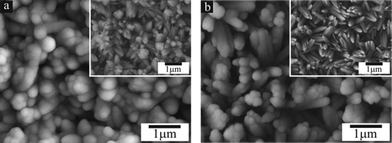
To elucidate the enhanced cycling stability and rate capability of the C-coated hollow SnO2 pillar arrays, we further observed the material using SEM and TEM after cycling. Fig. 7a shows a SEM image of delithiated C-coated hollow SnO2 pillars after 10 charge/discharge cycles. Interestingly, the electrode appears to maintain a pristine standing array structure without agglomeration of the SnO2 nanoparticles or pulverization of the pillar arrays. This observation demonstrates that aggregation of the nanoparticles can be inhibited by the 1D carbon-coated hollow geometry that constrains individual nanoparticle movement via effectively designed electrode configurations.26 The TEM image (Fig. 7b) shows that the thickness of the mesoscale tubules increased from approximately 60 to 100 nm after 10 cycles, while the hollow structure of the mesoscale tubules was maintained. Therefore, this C-coated hollow SnO2 array electrode can considerably suppress local stress gradients over that of a 1D hollow structure through a uniform volume change during Li+ alloying/dealloying, resulting in an inhibition of cracking or pulverization during cycling.
 | ||
| Fig. 7 Representative (a) SEM and (b) TEM images of the delithiated C-coated hollow SnO2 pillar array electrode after 10 cycles. | ||
Consequently, the highly stable cyclability and high rate performance of the C-coated hollow SnO2 pillar array electrode can be attributed to its unique structure and composition as follows: (i) the standing array structure can enable most of the C-coated hollow SnO2 pillars to participate in the electrochemical reactions because the entire SnO2 pillar arrays can be in electrical contact with the Ti current collector. (ii) Hollow channels along the 1D structure and nanopores formed from the collected SnO2 nanoparticles can accommodate the structural stress imposed during the Li+ alloying/dealloying processes. (iii) The porous nature of the SnO2 mesoscale tubules offers efficient electrolyte permeability and allows facilitated Li+ diffusion. (iv) The carbon shells help to electrically connect the SnO2 architectures to increase the charge transfer for the electrochemical reactions.
Conclusions
In conclusion, we have reported C-coated hollow SnO2 pillar arrays that are directly grown on a Ti substrate and can be utilized as an anode for LIBs without the addition of any ancillary materials, such as conductive carbon and cohesive binder. The C-coated hollow SnO2 array electrode showed a high initial discharge capacity (1251.9 mA h g−1), good cyclability, high rate capability and high coulombic efficiency. The enhanced cycling stability and high rate performance of the C-coated hollow SnO2 arrays are likely related to several of their unique structural features, such as their hollow architecture, which can mitigate strain energy, the porous structure assembled by the nanoparticles to increase electrolyte permeability, and the outer carbon layer to increase electrical connectivity. Thus, the C-coated hollow SnO2 pillar arrays, with high energy and power density, may justify their potential use as anode materials for next-generation LIBs that can electrochemically outperform current materials.Acknowledgements
This work was supported by the National Research Foundation (NRF) grant funded by the Ministry of Education, Science and Technology of Korea (MEST) (No. 20110016600) and by the Basic Science Research Program through NRF (No. R15-2008-006-03002-0). We also appreciate the financial support by the Global Frontier R&D Program (0420-20110157) on Center for Multiscale Energy System through NRF and by the Core Technology Development Program from the Research Institute of Solar and Sustainable Energies (RISE/GIST).References
- P. Poizot, S. Laruelle, S. Grugeon, L. Dupont and J.-M. Tarascon, Nature, 2000, 407, 496 CrossRef CAS.
- C.-M. Park, J.-H. Kim, H. Kim and H.-J. Sohn, Chem. Soc. Rev., 2010, 39, 3115 RSC.
- M. R. Palacin, Chem. Soc. Rev., 2009, 38, 2565 RSC.
- S. H. Nam, H.-S. Shim, Y.-S. Kim, M. A. Dar, J. G. Kim and W. B. Kim, ACS Appl. Mater. Interfaces, 2010, 2, 2046 CAS.
- Y. Shi, B. Guo, S. A. Corr, Q. Shi, Y.-S. Hu, K. R. Heier, L. Chen, R. Seshadri and G. D. Stucky, Nano Lett., 2009, 9, 4215 CrossRef CAS.
- Y. Idota, T. Kubota, A. Matsufuji, Y. Maekawa and T. Miyasaka, Science, 1997, 276, 1395 CrossRef CAS.
- X. W. Lou, C. M. Li and L. A. Archer, Adv. Mater., 2009, 21, 2536 CrossRef CAS.
- S. Han, B. Jang, T. Kim, S. M. Oh and T. Hyeon, Adv. Funct. Mater., 2005, 15, 1845 CrossRef CAS.
- J. G. Kim, S. H. Nam, S. H. Lee, S. M. Choi and W. B. Kim, ACS Appl. Mater. Interfaces, 2011, 3, 828 CAS.
- M.-S. Park, Y.-M. Kang, G.-X. Wang, S.-X. Dou and H.-K. Liu, Adv. Funct. Mater., 2008, 18, 455 CrossRef CAS.
- Z. R. Dai, J. L. Gole, J. D. Stout and Z. L. Wang, J. Phys. Chem. B, 2002, 106, 1274 CrossRef CAS.
- Y. Wang, J. Y. Lee and H. C. Zeng, Chem. Mater., 2005, 17, 3899 CrossRef CAS.
- P. Wu, N. Du, H. Zhang, J. Yu, Y. Qi and D. Yang, Nanoscale, 2011, 3, 746 RSC.
- N. Du, H. Zhang, B. Chen, X. Ma, X. Huang, J. Tu and D. Yang, Mater. Res. Bull., 2009, 44, 211 CrossRef CAS.
- W.-S. Kim, B.-S. Lee, D.-H. Kim, H.-C. Kim, W.-R. Yu and S.-H. Hong, Nanotechnology, 2010, 21, 245605 CrossRef.
- Y. Wang and J. Y. Lee, J. Phys. Chem. B, 2004, 108, 17832 CrossRef CAS.
- Q. Kuang, T. Xu, Z.-X. Xie, S.-C. Lin, R.-B. Huang and L.-S. Zheng, J. Mater. Chem., 2009, 19, 1019 RSC.
- J. Wang, N. Du, H. Zhang, J. Yu and D. Yang, J. Phys. Chem. C, 2011, 115, 11302 CAS.
- Y.-S. Hu, D.-C. Rezan, M.-M. Titirici, J.-O. Müller, R. Schlögl, M. Antonietti and J. Maier, Angew. Chem., Int. Ed., 2008, 47, 1645 CrossRef CAS.
- R. Huang, X. Fan, W. Shen and J. Zhu, Appl. Phys. Lett., 2009, 95, 133119 CrossRef.
- R. Demir-Cakan, M.-M. Titirici, M. Antonietti, G. Cui, J. Maier and Y.-S. Hu, Chem. Commun., 2008, 3759 RSC.
- G. Chen, Z. Wang and D. Xia, Chem. Mater., 2008, 20, 6951 CrossRef CAS.
- J. Yan, A. Sumboja, E. Khoo and P. S. Lee, Adv. Mater., 2011, 23, 746 CrossRef CAS.
- L. Yuan, J. Wang, S. Y. Chew, J. Chen, Z. P. Guo, L. Zhao, K. Konstantinov and H. K. Liu, J. Power Sources, 2007, 174, 1183 CrossRef CAS.
- C. K. Chan, X. F. Zhang and Y. Cui, Nano Lett., 2008, 8, 307 CrossRef CAS.
- Y. Li, B. Tan and Y. Wu, Nano Lett., 2008, 8, 265 CrossRef CAS.
- Y. Wang, H. C. Zeng and J. Y. Lee, Adv. Mater., 2006, 18, 645 CrossRef CAS.
- K. S. Han, J. W. Lee, Y. M. Kang, J. Y. Lee and J. K. Kang, Small, 2008, 4, 1682 CrossRef CAS.
- X. W. Lou, Y. Wang, C. Yuan, J. Y. Lee and L. A. Archer, Adv. Mater., 2006, 18, 2325 CrossRef CAS.
- Y.-D. Ko, J.-G. Kang, J.-G. Park, S. Lee and D.-W. Kim, Nanotechnology, 2009, 20, 455701 CrossRef.
- X. M. Yin, C. C. Li, M. Zhang, Q. Y. Hao, S. Liu, L. B. Chen and T. H. Wang, J. Phys. Chem. C, 2010, 114, 8084 CAS.
- Y. Wang, K. Takahashi, H. Shang and G. Cao, J. Phys. Chem. B, 2005, 109, 3085 CrossRef CAS.
- J. Liu, Y. Li, X. Huang, R. Ding, Y. Hu, J. Jiang and L. Liao, J. Mater. Chem., 2009, 19, 1859 RSC.
- J. Jiang, Y. Li, J. Liu and X. Huang, Nanoscale, 2011, 3, 45 RSC.
- W.-M. Zhang, X.-L. Wu, J.-S. Hu, Y.-G. Guo and L.-J. Wan, Adv. Funct. Mater., 2008, 18, 3941 CrossRef CAS.
- J. Liu, X. Huang, Y. Li, X. Ji, Z. Li, X. He and F. Sun, J. Phys. Chem. C, 2007, 111, 4990 CAS.
- J. Liu, C. Guo, C. M. Li, Y. Li, Q. Chi, X. Huang, L. Liao and T. Yu, Electrochem. Commun., 2009, 11, 202 CrossRef CAS.
- M. Noh, Y. Kwon, H. Lee, J. Cho, Y. Kim and M. G. Kim, Chem. Mater., 2005, 17, 1926 CrossRef CAS.
- F. Cheng, Z. Tao, J. Liang and J. Chen, Chem. Mater., 2008, 20, 667 CrossRef CAS.
- H.-W. Liang, S. Liu and S.-H. Yu, Adv. Mater., 2010, 22, 3925 CrossRef CAS.
- S. H. Lee, G. Jo, W. Park, S. Lee, Y.-S. Kim, B. K. Cho, T. Lee and W. B. Kim, ACS Nano, 2010, 4, 1829 CrossRef CAS.
- Y. Wang and G. Cao, J. Mater. Chem., 2007, 17, 894 RSC.
- Y. Wang, K. Takahashi, H. Shang and G. Cao, J. Phys. Chem. B, 2005, 109, 3085 CrossRef CAS.
- S. M. Choi, M. H. Seo, H. J. Kim and W. B. Kim, Carbon, 2011, 49, 904 CrossRef CAS.
- Z. Yang, G. Du, Z. Guo, X. Yu, Z. Chen, P. Zhang, G. Chen and H. Liu, J. Mater. Res., 2011, 25, 1516 CrossRef.
- Y. Liu and M. Liu, Adv. Funct. Mater., 2005, 15, 57 CrossRef.
- X. W. Lou, J. S. Chen, P. Chen and L. A. Archer, Chem. Mater., 2009, 21, 2868 CrossRef CAS.
- J. Liu, Y. Li, R. Ding, J. Jiang, Y. Hu, X. Ji, Q. Chi, Z. Zhu and X. Huang, J. Phys. Chem. C, 2009, 113, 5336 CAS.
- S. T. Chang, I. C. Leu, C. L. Liao, J. H. Yen and M. H. Hon, J. Mater. Chem., 2004, 14, 1821 RSC.
- R. Demir-Cakan, Y.-S. Hu, M. Antonietti, J. Maier and M.-M. Titirici, Chem. Mater., 2008, 20, 1227 CrossRef CAS.
- H. Wang, Q. Pan, Y. Cheng, J. Zhao and G. Yin, Electrochim. Acta, 2009, 54, 2851 CrossRef CAS.
- M.-S. Park, G.-X. Wang, Y.-M. Kang, D. Wexler, S.-X. Dou and H.-K. Liu, Angew. Chem., Int. Ed., 2007, 119, 764 CrossRef.
- M. Xu, M. Zhao, F. Wang, W. Guan, S. Yang and X. Song, Mater. Lett., 2010, 64, 921 CrossRef CAS.
- S.-L. Chou, J.-Z. Wang, H.-K. Liu and S.-X. Dou, Electrochem. Commun., 2009, 11, 242 CrossRef CAS.
- S. H. Nam, K. S. Kim, H.-S. Shim, S. H. Lee, G. Y. Jung and W. B. Kim, Nano Lett., 2011, 11, 3656 CrossRef CAS.
- L. Li, X. Yin, S. Liu, Y. Wang, L. Chen and T. Wang, Electrochem. Commun., 2010, 12, 1383 CrossRef CAS.
- R. A. Huggins, Advanced Batteries. Materials Science Aspects, Springer: New York, 2009 Search PubMed.
- G. Chen, Z. Wang and D. Xia, Chem. Mater., 2008, 20, 6951 CrossRef CAS.
Footnote |
| † Electronic supplementary information (ESI) available: XPS spectra of C-coated SnO2 and additional electrochemical data. See DOI: 10.1039/c2ra21218h/ |
| This journal is © The Royal Society of Chemistry 2012 |