Micro/nanoporous polymer chips as templates for highly sensitive SERS sensors
Suzanna
Akil-Jradi
*,
Safi
Jradi
*,
Jérôme
Plain
,
Pierre-Michel
Adam
,
Jean-Louis
Bijeon
,
Pascal
Royer
and
Renaud
Bachelot
Laboratoire de Nanotechnologie et d'Instrumentation Optique, Institut Charles Delaunay, STMR-UMR6279 CNRS, Université de Technologie de Troyes, 12 Rue Marie Curie BP 2060, F-10010 Troyes cedex. E-mail: suzanna.jradi@utt.fr; safi.jradi@utt.fr
First published on 21st June 2012
Abstract
High-throughput, simple nanofabrication methods are essential keys for involving plasmonic materials with large electric fields for practical applications. We demonstrate in this paper a facile route for fabricating multifunctional metallic nanomaterials for sensing, which is particularly relevant to SERS spectroscopy. A simple deposition of a polymer dispersion doped with metallic precursor onto a conducting substrate allows a spontaneous formation of SERS-active substrates via vapor induced phase separation. The process enables the fabrication of several kinds of SERS chips with an original combination of fast throughput, low cost, reproducibility and high sensitivity. Our SERS results show significant enhancement factors exceeding 1013, which match the largest value (1014) of metallic nanoparticle aggregates found until now. We quantify these enhancements by depositing bipyridine ethylene (BPE) on the substrate and spatially mapping their Raman intensities using confocal micro-Raman spectroscopy. Both the sensitivity threshold and reproducibility of all substrates were estimated by SERS measurements at variable concentrations of BPE. Our approach is new in fabricating high-throughput and reproducible SERS substrates over a large surface (on the whole substrate) by a one-step technique. As a result, we demonstrate a novel class of SERS substrates for which no patterning is necessary as in lithography, which provide a quick, simple and cheap way to fabricate highly sensitive SERS substrates.
Introduction
Plasmonic materials exhibiting distinct surface-plasmon-resonance effects have gained increasing attention over the last few years1,2 due to their broad applications, including electronics,3 photonics,4,5 catalysis,6 biological imaging,7,8 drug delivery, sensors and surface enhanced Raman scattering (SERS).9–11 One of the main drivers for the development of plasmonic materials by various processes is the desire to improve the sensitivity of SERS for exploring structure and reaction pathways at surfaces, as well as for sensing.12 SERS is currently one of the most promising ways to enhance the optical fields of noble metal nanostructures from Raman-active analyte molecules that have been adsorbed onto metal surfaces.13,14 Furthermore, the sensitivity of SERS measurements is one of the highest among analytical techniques15 since the Raman signal enhancement can reach 1014, which is sufficient to detect a single molecule.16 Such a high value of SERS enhancement has been achieved using rough metal electrodes and aggregates of MNPs with extremely small interparticle spaces (nanogaps).17,18 Currently, SERS is the basis of biosensing techniques due to its reliability, rapidity and ease of operation as compared with other analysis methods.15 The interest in SERS also comes from its high sensitivity and surface selectivity, which enable the investigation of a wide variety of systems such as electrochemical, catalytic, biological and organic molecules.19–21Over a wide range of studies, the challenge is to develop substrates combining high sensitivity and localization of hot spots, regions where the electromagnetic field is locally concentrated, leading to a high SERS enhancement.22 The SERS substrates also should demonstrate high reproducibility, stability and ease of preparation. To make it possible, tailoring and fine-tuning of the size, shapes, roughness, composition and interparticle separations of metal nanoparticles is crucial for SERS applications.23–25 In this context, the recent decade has witnessed enormous research efforts to create new SERS-active substrates.26 Thus, a wide range of geometries, like nanoparticle arrays, rods, cubes, prisms, wires, tubes, branches, sheets, bowtie antennas, nanoshells, nanoaperture arrays, nanogaps and nanorings were recently investigated.27,28 There are several methods for the formation of such nanostructure shapes, including porous films,29 colloidal assembly,30 electron-beam lithography,31 nanosphere lithography32 and radical mediated photoreduction.33 Nanolithography is currently one of the most reproducible methods for the fabrication of SERS substrates with controlled hot spots,34 owing to an accurate control of the shape, size and morphology of structures. However, lithographic materials are costly and require expensive technological steps and trained personnel for the fabrication, which result in a low-throughput. In addition, up to now lithography provides Raman enhancements of 104–106, in relation with a limitation in the size of structures (≥10 nm).35,36 On the other hand, chemically fabricated substrate patterns can be easily prepared, producing lower sizes (1–5 nm) and providing strong Raman enhancements (1012–1014).37 Nevertheless, such substrates are typically random and difficult to reproduce due to the difficulty in establishing a good repetition of hot spots on the surface. In addition, a step of substrate functionalization is usually necessary to prevent an aggregation of the MNPs upon deposition on the substrate.
Many studies have shown that hot spots, increasing the Raman enhancement, are located in the junction between two closely spaced metallic nanostructures.38,39 Therefore, a large amount of SERS research is currently focused toward fabricating nanogap structures via the methods assessed above. However, the production of sub-10 nm gaps via simple nanofabrication techniques combining high-throughput, high-resolution and low cost is crucial for practical SERS applications and remains a significant challenge.
In this context, we report a new technique combining reproducibility and high enhancement based simultaneously on the vapor-induced phase separation (VIPS) and chemical reduction of a metal precursor-doped polymer dispersion. The VIPS is attributed to polymer self-assembly due to the different evaporation rates of polymer solvent and non-solvent.40 This phenomenon for block copolymer templating has recently gained significant technological importance due the possibility to fabricate nanostructures in a simple manner.41 However, this technique emphasizes the synthesis of functional hybrid materials (polymer/metal) and no attention is paid to metallic nanoparticles fabricated via this method and the SERS of such nanostructures has not been investigated. It is noteworthy that the VIPS process is relatively not fast and simple because of the step of synthesis of block copolymers and the temperature reduction of metallic precursor that is generally required to produce the nanostructures.
From there, our purpose is to provide highly reproducible nanogaps on-chip SERS through a spontaneous VIPS and then to develop this method for sensing applications. To make it possible, polymethtyl methacrylate (PMMA) vesicles loaded with metallic precursor (Ag+ in our case) were prepared in solution and porous or honeycomb structures were produced via VIPS upon spin-coating on a conducting substrate. A schematic representation of this experimental approach is shown is Scheme 1. Here, it is interesting to observe different shapes of MNPs in relation to the shape of PMMA particles that depends on the VIPS conditions (chemistry of the polymer solution and the substrate nature).
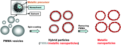 | ||
| Scheme 1 A schematic representation of the fabrication process of SERS chips. | ||
Experimental
Substrates fabrication
The PMMA/silver dispersion was made by mixing solutions of silver precursor and PMMA. The silver solution was prepared by dissolution of 50 mg of AgNO3 in 2 ml of ethanol. Subsequently, 2 ml of PMMA/acetone solution was added to the metallic solution while being stirred at 300 rpm for 1 h. The resulting solution was deposited by spin-coating on a conducting substrate. As a result, a large-scale SERS substrate of small nanoparticles interspaced with super nanogaps (≤10 nm) were obtained, as shown in Scheme 1.Surface-enhanced Raman scattering (SERS) experiments
The performance of our SERS substrates was evaluated on the bipyridine ethylene (BPE) using a Jobin Yvon LabRam instrument equipped with a laser operating at 633 nm and 11 mW power in a back reflection mode. The data were acquired with a 50× objective (N. A. 0.8).Results and discussion
As the substrate conductivity seems to play a major role in the spontaneous formation of MNPs, we tried to change this property using a semi-conducting substrate (silicon) and a conducting one by deposition of Indium Tin Oxide (ITO) on glass. It is expected that the conducting surface provides electrons to the metallic precursor and then allows the fabrication of metallic nanoparticles upon a simple electroless reduction of metallic salt via the reaction: Mn+ + ne− → M (M corresponds to metal). This phenomenon has been described by Kalkan et al.42 and investigated by Bhatt et al.43 in the study of charge-selective SERS and fluorescence. Therefore, no particles are formed in solution since no conducting compound is present here to pass the electrons to Ag+ ions. Consequently, the formation of metallic nanoparticles occurs just on the substrate surface upon coating the PMMA/Ag+ solution resulting in solvent evaporation, which disturbs its stability and provides then the formation of polymer holes. For this reason, the MNPs must be firmly attached to the surface and their distribution, size and shape are strongly dependent on the surface (hydrophobicity, charges distribution, charges concentration, etc.).As assessed above, controlling the optical and physical properties of MNPs provides a powerful tool to fabricate tailored SERS nanostructures. In our case, this control is mainly dominated by the self-assembly phenomenon and the substrate (conductivity, surface energy and chemistry, etc.). In this context, it is crucial to tune the chemical interactions at the solvent–particle interface by adjusting the volume ratio of solvent to non-solvent. Also, the ionic strength related to the metallic precursor concentration is to be considered. On this basis, we tried to modify such parameters to obtain various morphologies of nanostructures, which allow us to modulate the SERS features. On this basis, we investigated the role of the substrate on the nanoparticles morphologies. First, silver nanoholes are spontaneously formed upon spin-coating of Ag+ doped PMMA particles on a silicon wafer, as shown in Fig. 1a. The SEM image in Fig. 2a reveals sub-10 nm gaps nanoparticles along the perimeter of nanorings. To get more information about the distribution of silver nano-objects into the polymer layer, AFM imaging has been done. Fig. 2b and c show narrow size distribution of nanoholes and highlight the presence of silver nanorings (white ring) along the contour of polymer pores. Subsequently, the polymer matrix is extracted by acetone leaving behind purely silver nanostructures as shown in Fig. 2. The inserts in Fig. 2a and b reveal the presence of Ag nanoholes after removing the PMMA, which is confirmed by the decrease of ring thickness. It is interesting to observe that MNPs retain the same ring shape without the polymer matrix, which reflects their high adhesion to the substrate and highlights the original morphology of PMMA film as the template. Moreover, no stabilizer is necessary here as compared to the colloidal synthesis. This property is of a great interest, since removing this stabilizer could disturb the morphology of the nanostructures, which is an inconvenience in most synthesis methods of MNPs.
 | ||
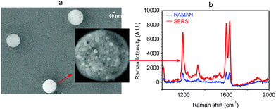
| Fig. 1 (a) A SEM image of Ag nanorings synthesized on silicon. (b) An AFM image of the same substrate. (c) An AFM profile of the corresponding image. | ||
 | ||
| Fig. 2 A SEM image of porous Ag nanostructures obtained by spin-coating of PMMA/Ag+ dispersion on a silicon substrate and the corresponding profile: (a) with PMMA and (b) after removing PMMA. | ||
In order to evaluate the substrate efficiency in SERS detection, a 50 μl droplet at a concentration of 10−5 M of bipyridine–ethylene (BPE) was deposited on the surface of the substrate in Fig. 2. SERS measurements were made after the evaporation of water from the drop to achieve a good adsorption of BPE on the substrate. To be able to estimate the enhancement factor of our substrates, which will be discussed in the next section, we compared our thin PMMA/metal film samples to PMMA film with the same thickness. Also, the Raman data were acquired with 3 orders of magnitude lower BPE concentration (10−2 M) and during 10 s against 10−5 M and 1 s for SERS in the same optical conditions.
Fig. 3c shows a strong SERS signal as compared to Raman, which reflects a high sensitivity of the corresponding substrate since the integration time and the BPE concentration were lower for SERS measurements. The reason for such a high enhancement can be attributed to the hydrophobic layer of PMMA that allows a selective accumulation of BPE onto the metallic regions of the substrate. Fig. 3 presents a schematic illustration of the BPE distribution on the surface of substrate. We suggest that repulsive interactions between PMMA (hydrophobic) and BPE (hydrophilic) molecules directs them to move to the Ag nanoparticles, which focuses the SERS onto nano-zones and then leads to high enhancement. It is worth noting that BPE droplet spreads directly on the substrate surface if we remove PMMA, in relation with lower SERS enhancement (Fig. 3c). Recently, De Angelis et al.44 showed that combining super-hydrophobic surfaces and plasmonic nanofocusing SERS allows them to overcome the diffusion limit when sensors approach a nanoscale length and to detect few molecules. This might be our case where the PMMA matrix plays a major role in the high SERS nanofocusing and enhancement. It must be noticed that the high enhancement factors of all of the substrates shown above were obtained with and without the PMMA layer (see Fig. 2 and 3). Although the substrates reveal higher enhancement in the presence of PMMA due to the hydrophobic property of this film, the ultra-sensitivity of substrates results mainly from a high hot spots concentration on a large surface. In addition, SERS measurements were also made on a liquid droplet of BPE, revealing 3 times lower SERS intensity (results not shown). Thus, a still high sensitivity and the same order of magnitude for the SEF is maintained in the presence of the coffee rings.
 | ||
| Fig. 3 (a) and (b) AFM images of Ag nanorings obtained in Fig. 1 illustrating the accumulation of BPE at the metallic contour upon the deposition of the drop. (c) SERS and Raman spectra of BPE for the same substrate. | ||
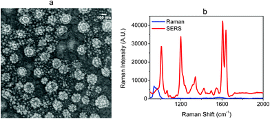
To fully exploit the advantage of our approach, we changed the substrate to show the versatility in the elaboration of a various number of substrates. Thus, the nanorings shown above are completely filled by the nanoparticles to achieve a nano corn-flake shape when silicon is replaced by ITO-coated glass. Fig. 4a shows a continuous nanometric gap between nanoparticles in a given flake. Conducting sites are present on the whole ITO surface and might attract silver ions upon the spin-coating of PMMA solution and lead them to fill the vesicle volume, which is hydrophilic and then compatible with silver. After solvent evaporation, the high conductivity of ITO allows the reduction of a maximum number of silver ions. Consequently, randomly shaped and sized nanoparticles were formed and assembled into selective regions on the substrate (flakes). The low gap between these nanoparticles (<10 nm) and their high density on the substrate gave rise to higher SERS enhancement, as shown in Fig. 4b. Furthermore, we could detect down to 10−10 M of BPE using these structures, in relation to a lower time of measurement and then higher substrate sensitivity. It is worth noting that the number of corn-flakes seen by the laser beam (50× objective) greatly increases with the addition of more PMMA layers, as we can see in Fig. 7. We can also talk about intra- and inter-particle distances versus the corn-flakes, which induces hot spots concentration in the SERS confocal volume of measurement and then results in higher SERS Enhancement Factor (SEF).
 | ||
| Fig. 4 (a) SEM images of Ag nano corn-flakes fabricated on ITO-coated glass. (b) SERS of 10−5 M and 10−10 M of BPE obtained on the corresponding nano corn-flakes. | ||
As a second example, we report the ability to fabricate other nanoparticle morphologies on both the micro- and nano scales by changing the substrate nature. As a result, submicrometer plots were obtained by hydrophobically (–CH3 groups) functionalizing the glass substrate (Fig. 5a). Since the metallic structures are relatively spaced, we were able to make SERS measurements on a single nanocluster, as shown in the insert of Fig. 5a.
 | ||
| Fig. 5 (a) SEM images of Ag nanocluster fabricated on functionalized glass. (b) The SERS spectrum of 10−5 M of BPE obtained from a single nanocluster. The Raman spectrum was made with 10−2 M of BPE. | ||
In Fig. 5b, we present the SERS spectrum for one nanocluster performed after an acquisition time of 1 min with a BPE concentration of 10−4 M. It is interesting to observe the lower SERS enhancement of this kind of substrate, which is expected since measurements were collected from a single cluster.
So far we have presented spontaneously fabricated nanostructures without any treatment of the substrate after deposition of the polymer layer. Other particle geometries could also be realized by simply heating the substrate after fabrication to reduce silver ions that have not yet been reduced on surface. Thus, the nano corn-flakes seen in Fig. 4a became nanoflowers (Fig. 6a) after treatment at a temperature of 70 °C for 15 min. One can see the larger size of nanoparticles for a given plot, which can be attributed to a particles aggregating upon heating. Therefore, Fig. 5b reveals the lower SERS enhancement of these nanoflowers, which validates our one-shot process since no post-treatment is necessary to obtain a good SERS enhancement.
 | ||
| Fig. 6 (a) SEM images of Ag nanoflowers fabricated on ITO-coated glass after heating the nano corn-flakes at 70 °C for 15 min. (b) The SERS spectrum of 10−5 M of BPE obtained on the corresponding substrate. The Raman spectrum was made with 10−2 M of BPE. | ||
To go further in the sensitivity of these structures, we tried to decrease the interparticle spaces by decreasing the density of nanoparticles on the substrate via a successive deposition of several layers of PMMA solution. Fig. 7a shows the higher density of corn-flakes after 10 successive spin-coatings of PMMA solution on ITO-coated glass, in relation with low gaps into each plot and between two plots. It is interesting to observe a double ring shape for each cluster that might enhance the Raman signal.
 | ||
| Fig. 7 (a) SEM images of Ag nano corn-flakes fabricated on ITO-coated glass. (b) The SERS spectrum of 10−7 M of BPE obtained on the corresponding substrate. The Raman spectrum was made with 10−2 M of BPE. | ||
In the same optical conditions, this substrate revealed more sensitivity, since 0.5 s was sufficient to get a better signal to noise ratio. Moreover, it was necessary to decrease the concentration until 10−7 M to keep the experimental conditions constant and then to be able to compare Raman to SERS. Consequently, a higher SERS signal was obtained with an increasing number of nanoparticles on the substrate, as shown in Fig. 7b.
This substrate exhibits the highest SERS enhancement as compared to the other ones. To highlight this result, we estimated the SERS enhancement factor (SEF) of each substrate. The SEF was determined following a procedure established in the literature.26,45 We employed the Raman band of 1605 cm−1 to calculate the SEF through the following equation :
| SEF = (ISERS × Nnormal)/(Inormal × NSERS) | (1) |
where ISERS and Inormal are the intensities of the same band for the SERS and normal Raman spectra, Nnormal is the number of molecules probed for a normal Raman setting and NSERS is the number of molecules probed in SERS.
N normal and NSERS values were calculated taking into account the density of the surface species or bulk sample and the corresponding sampling areas. Moreover, each nanoparticle was considered as a hemisphere i.e. half-sphere shape in this calculation. We chose this band because it was the strongest band in the spectra. Nnormal was determined based on the Raman spectrum of a 10−2 M BPE solution. The focal volume of our Raman system is 10.6 fl. The SERS confocal volume corresponds to 1.44 × 10⁻³ fl, taking into account the size of nanoparticles for a given substrate. These volumes allow the detection of 3 × 10⁶ molecules in Raman and 4 × 10² molecules in SERS for a concentration of 10−5 M, taking into account the number of particles in the SERS focal volume. Regarding the low acquisition time (1 s) that provides a high signal to noise ratio, it was possible to go further down than 10−5 M to get an idea about the sensitivity threshold of all the substrates.
On this basis, we calculated SEF of the different substrates illustrated above for a fixed BPE concentration of 10−7 M. For all substrates, the SEF is ∼108 and it reaches 1013 for the high-density nano corn-flakes (smallest nanogaps). It must be noticed that the SEF calculation is usually done with a great number of approximations. Therefore, we preferred to evaluate the sensitivity of our substrate in terms of the efficiency of low concentration detection. Thus, we tried to estimate the threshold detection i.e. the lowest concentration of BPE that can be detected by a given substrate. Solutions of progressively decreasing concentration were investigated as a function of the substrate sensitivity. The evolution of SERS intensity for the 1605 cm−1 band was then plotted vs. the BPE concentration in Fig. 8, which highlights the sensitivity limit of the substrate. A sensitivity threshold of 10−12 M was determined, which is an unprecedented low value in the detection of BPE. Until now, the lowest BPE concentration detected was 10−9 M, which corresponds to an EF of ∼5 × 10⁹ as determined by the authors.46 Moreover, Driskell et al.47 showed an EF of ∼108 at 10−8 M of BPE and considered the 10−12 M as a limiting value for BPE detection.
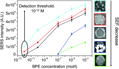 | ||
| Fig. 8 The evolution of the SERS intensity at 1605 cm−1 as a function of BPE concentration for the different substrates. | ||
As assessed above, our lowest BPE concentration detected is 10−12 mol l−1 and gave rise a SEF value that matches the largest enhancements (1014) of nanoshells and nanoparticle aggregates.15–18 Large SERS enhancement factors and size effects in the optical properties of MNPs have also been observed by other groups.45–49 In our case, the low gap effects play a major role in the large SERS response.48,49 It is clearly revealed that despite the randomly distributed nanostructures or hot spots, SERS results are reproducible for a given substrate and for several substrates of the same kind. To get a better idea about this reproducibility, we illustrate in Fig. 9 an histogram representation of the SERS intensity variation from the 1605 cm−1 band for all of the substrates prepared.
 | ||
| Fig. 9 A schematic view of the reproducibility of SERS measurements for all substrates. | ||
Experiments were repeated for substrates from different batches and all exhibited high sensitivity and reproducibility, as mentioned above. A remarkably small intensity variation highlights a reproducibility of ∼90%, which could be the least among the previously reported substrates fabricated by various techniques.15–18,43 These findings are promising, especially for sensing since it is always challenging to have a SERS substrate with adequate signal enhancement and lower intensity variation.
Let us consider the SERS spectrum of BPE to get a better understanding of the physical features of the nanostructures. The observed Raman and SERS spectra are in good agreement with those reported in the literature.50–52 The SERS bands are blue shifted as compared to the Raman spectra, except for the 1092 cm−1 band, which is red shifted. These shifts are most likely due to the interaction between BPE and silver nanoparticles. Referring to a large number of works, we could identify these peaks45–49 in the following manner: the peak at 1200 cm−1 is assigned to the ring breathing mode of BPE pyridine that includes the vibrational movement of the pyridyl nitrogen atom. The peak observed at 1609 cm−1 is assigned to the C–N stretching mode of the pyridyl ring, which also includes the movement of the pyridyl nitrogen atom. The band at 1635 cm−1 involves the vibration of the vinyl group within BPE. The peak at 1025 cm−1 can be attributed to the chemisorption of BPE to Ag nanoparticles based on different works and our results.45–49 Even the experimental conditions (time, BPE concentration) were different for the overall substrates; one can see a change in the intensity and position of the 1025 cm−1 if the substrate changes. The observed frequency shifts might be an indication that a chemical component is present and provides the interaction of BPE with the substrate through a charge transfer complex. As an example, this peak disappeared in Fig. 6b where heating the substrate must reduce silver ions present on its surface and then decreases the number of charges able to interact with the BPE. Like many situations in SERS, we suggest that a part of the large EF obtained is due to the chemical enhancement.50 This is a statement that has been investigated several times in the literature in different contexts, but never with proper justification through a specific quantitative example as in our case, where much effort is still needed for complete understanding of the optical properties of these complex nanostructures.
Conclusions
The presented results demonstrate a simple, flexible, cheap and highly versatile approach to fabricate metallic nanomaterials for SERS detection. In addition to their high throughput, we demonstrated ultra sensitive and reproducible SERS substrates with an enhancement factor that matches 1014, which is the maximum reported in the literature until now. Such high sensitivity could be interesting for the detection of a few molecules in a highly diluted solution in fields including biomedicine, safety and environmental pollution in relation to rare and dangerous chemicals. We can also talk about multifunctional nanostructures to be used widely for sensing by tuning the vapor induced phase separation of hybrid materials. The same approach could be used to incorporate a variety of inorganic components (metallic, photonic, etc.) selectively into the PMMA vesicles by simply changing the type of precursor in order to fabricate different hybrid/homo materials.Acknowledgements
This work was supported by Nano'Mat, Platform of Nanostructuring and Nanomaterials characterization at the region of Champagne-Ardennes in France. We acknowledge Nano'Mat (www.nanomat.eu) for its financial support made by the Ministère de l'enseignement supérieur et de la recherche, the Conseil régional Champagne-Ardenne, the FEDER funds and the Conseil général de l'Aube.References
- E. Ozbay, Science, 2006, 311, 189 CrossRef CAS.
- S. Maier, Plasmonics: Fundamentals and Applications, Springer, New York, 2007 Search PubMed.
- J. H. Lee, D. O. Kim, G. S. Song, Y. Lee, S. B. Jung and J. D. Nam, Macromol. Rapid Commun., 2007, 28, 634 CrossRef CAS.
- M. J. Li, H. Zhang, J. H. Zhang, C. L. Wang, K. Han and B. J. Yang, J. Colloid Interface Sci., 2006, 300, 564 CrossRef CAS.
- S. Kubo, Z. Z. Gu, D. A. Tryk, Y. Ohko, O. Sato and A. Fujishima, Langmuir, 2002, 18, 5043 CrossRef CAS.
- T. Ishida, K. Kuroda, N. Kinoshita, W. Minagawa and M. J. Haruta, J. Colloid Interface Sci., 2008, 323, 105 CrossRef CAS.
- L. R. Hirsch, A. M. Gobin, A. R. Lowery, F. Tam, R. A. Drezek, N. J. Halas and J. L. West, Ann. Biomed. Eng., 2006, 34, 15 CrossRef.
- T. M. Lee, A. L. Oldenburg, S. Sitafalwalla, D. L. Marks, W. Luo, F. J. J. Toublan, K. S. Suslick and S. A. Boppart, Opt. Lett., 2003, 28, 1546 CrossRef CAS.
- S. Akil-Jradi, S. Jradi, J. Plain, J.-L. Bijeon, C. Sanchez, R. Bachelot and P. Royer, Chem. Commun., 2011, 47, 2444 RSC.
- A. Shamsaiea, J. Heima, A. A. Yanik and J. Irudayaraj, Chem. Phys. Lett., 2008, 461, 131 CrossRef.
- J. A. Dieringer, R. B. Lettan, K. A. Scheidt and R. P. Van Duyne, J. Am. Chem. Soc., 2007, 129, 16249 CrossRef CAS.
- S. J. Lee, B. D. Piorek, C. D. Meinhart and M. Moskovits, Nano Lett., 2010, 10, 1329 CrossRef CAS.
- E. M. Prodan, C. Radloff, N. J. Halas and P. Nordlander, Science, 2003, 302, 419 CrossRef CAS.
- W. L. Barnes, A. Dereux and T. W. Ebbesen, Nature, 2003, 424, 824 CrossRef CAS.
- K. Kneipp, Y. Wang, H. Kneipp, L. T. Perelman, I. Itzkan, R. R. Dasari and M. S. Feld, Phys. Rev. Lett., 1997, 78, 1667 CrossRef CAS.
- S. M. Nie and S. R. Emory, Science, 1997, 275, 1102 CrossRef CAS.
- V. M. Shalaev, Phys. Rep., 1996, 272, 61 CrossRef CAS.
- E. Hao and G. C. J. Schatz, Chemical Physics, 2004, 120, 357 CAS.
- K. Kneipp, Y. Wang, R. R. Dasari, M. S. Feld, B. D. Gilbert, J. Janni and J. I. Steinfeld, Spectrochim. Acta, Part A, 1995, 51, 2171 CrossRef.
- Y. C. Cao, R. Jin and C. A. Mirkin, Science, 2002, 297, 1536 CrossRef CAS.
- S. Shanmukh, L. Jones, J. Driskell, Y. Zhao, R. Dluhy and R. A. Tripp, Nano Lett., 2006, 6, 2630 CrossRef CAS.
- M. Käll, H. Xu and P. J. Johansson, J. Raman Spectrosc., 2005, 36, 510 CrossRef.
- K. Kneipp, H. Kneipp, I. Itzkan, R. R. Dasari and M. S. Feld, Chem. Rev., 1999, 99, 2957 CrossRef CAS.
- J. Grand, M. L. de la Chapelle, J. L. Bijeon, P. M. Adam, A. Vial and P. Royer, Phys. Rev. B., 2005, 72, 033407 CrossRef.
- L. Gunnarsson, E. J. Bjerneld, H. Xu, S. Petronis, B. Kasemo and M. Kall, Appl. Phys. Lett., 2001, 78, 802 CrossRef CAS.
- C. L. Haynes and R. P. Van Duyne, J. Phys. Chem. B, 2001, 105, 5599 CrossRef CAS.
- K. Kneipp, H. Kneipp and J. Kneipp, Acc. Chem. Res., 2006, 39, 443 CrossRef CAS.
- Y. Fang, N.-H. Seong and D. D. Dlott, Science, 2008, 321, 388 CrossRef CAS.
- L. H. Qian, X. Q. Yan, T. Fujita, A. Inoue and M. W. Chen, Appl. Phys. Lett., 2007, 90, 153120 CrossRef.
- M. I. Stockman, V. M. Shalaev, M. Moskovits, R. Botet and T. F. George, Phys. Rev. B, 1992, 46, 2821 CrossRef.
- Y. J. Liu, Z. Y. Zhang, Q. Zhao and Y. P. Zhao, Appl. Phys. Lett., 2008, 93, 173106 CrossRef.
- H. Fredriksson, Y. Alaverdyan, A. Dmitriev, C. Langhammer, D. S. Sutherland, M. Zach and B. Kasemo, Adv. Mater., 2007, 19, 4297 CrossRef CAS.
- S. Jradi, L. Balan, X. Zeng, J. Plain, D.-J. Lougnot, P. Royer, R. Bachelot, S. Akil, O. Soppera and L. Vidal, Nanotechnology, 2010, 21, 095605–1 CrossRef.
- T. R. Jensen, M. D. Malinsky, C. L. Haynes and R. P. Van Duyne, J. Phys. Chem. B, 2000, 104, 10549 CrossRef CAS.
- D. U. Soudamini, F. C. Yaw, A. Agarwal and M. Olivo, Biosensors & Bioelectronics, 2010, 26, 1987 Search PubMed.
- Q. Yu, P. Guan, D. Qin, G. Golden and P. M. Wallace, Nano Lett., 2008, 8, 1923 CrossRef CAS.
- A. Gopinath, S. V. Boriskina, N.-N. Feng, B. M. Reinhard and L. D. Negro, Nano Lett., 2009, 8, 2423 CrossRef.
- H. Im, K. C. Bant, N. C. Lindquist, C. L. Haynes and S.-H. Oh, Nano Lett., 2010, 10, 2231 CrossRef CAS.
- K. Bhatt, S. Tan, S. Karumuri and A. K. Kalkan, Nano Lett., 2010, 10, 3880 CrossRef CAS.
- X. D. Zhou, S. C. Zhang, W. Huebner and P. D. Ownby, J. Mater. Sci., 2001, 36, 3759 CrossRef CAS.
- D. E. Discher and A. Eisenberg, Science, 2002, 297, 967 CrossRef CAS.
- A. K. Kalkan and S. J. Fonash, J. Phys. Chem. B, 2005, 109, 20779 CrossRef CAS.
- K. Bhatt, S. Tan, S. Karumuri and A. K. Kalkan, Nano Lett., 2010, 10, 3880 CrossRef CAS.
- F. De Angelis, F. Gentile, F. Mecarini, G. Das, M. Moretti, P. M. Candeloro, L. Coluccio, G. Cojoc, A. Accardo, C. Liberale, R. P. Zaccaria, G. Perozziello, L. Tirinato, A. Toma1, G. Cuda, R. Cingolani and E. Di. Fabrizio, Nat. Photonics, 2011, 5, 682 CrossRef CAS.
- S. M. Wells, S. D. Retterer, J. M. Oran and M. J. Sepaniak, ACS Nano, 2009, 3, 3845 CrossRef CAS.
- E. J. Blackie, E. C. Le Ru and P. G. Etchegoin, J. Am. Chem. Soc., 2009, 131, 14466 CrossRef CAS.
- J. D. Driskell, S. Shanmukh, Y. Liu, S. B. Chaney, X.-J. J. tang, Y.-P. Zhao and R. A. Dluhy, J. Phys. Chem. C, 2008, 112, 895 CAS.
- A. D. McFarland, M. A. Young, J. A. Dieringer and R. P. Van Duyne, J. Phys. Chem. B, 2005, 109, 11279 CrossRef CAS.
- N. A. Hatab, C.-H. Hsueh, A. L. Gaddis, S. T. Retterer, J.-H. Li, G. Eres, Z. Zhang and B. Gu, Nano Lett., 2010, 10, 4952 CrossRef CAS.
- J. C. Hulteen, M. A. Young and R. P. Van Duyne, Langmuir, 2006, 22, 10354 CrossRef CAS.
- L. A. Dick, A. D. McFarland, C. L. Haynes and R. P. Van Duyne, J. Phys. Chem. B, 2002, 106, 853 CrossRef CAS.
- P. M. Tessier, O. D. Velev, A. T. Kalambur, J. F. Rabolt, A. M. Lenhoff and E. W. Kaler, J. Am. Chem. Soc., 2000, 122, 9554 CrossRef CAS.
| This journal is © The Royal Society of Chemistry 2012 |