Rectifying behaviors of an Au/(C20)2/Au molecular device induced by the different positions of gate voltage
Guomin
Ji
a,
Yuqing
Xu
a,
Bin
Cui
a,
Changfeng
Fang
b,
Xiangru
Kong
a,
Dongmei
Li
a and
Desheng
Liu
*ac
aSchool of Physics, State Key Laboratory of Crystal Materials, Shandong, University, Jinan 250100, People's Republic of China
bDivision of Computational Physics IFM, Linköping University, SE-581 83, Linköping, Sweden
cDepartment of Physics, Jining University, Qufu 273155, People's Republic of China. E-mail: liuds@sdu.edu.cn
First published on 20th September 2012
Abstract
The electronic transport properties of a gated Au/(C20)2/Au molecular device are studied using nonequilibrium Green's function in combination with density functional theory. The results show that different applied positions of the external transverse gate voltage can effectively tune the current–voltage (I–V) characteristic of molecular devices. Rectifying behaviors of the device can be realized when the gate voltage is applied asymmetrically on the left C20 molecule, and the rectification directions can also be modulated by the positive or negative value of the gate voltage. These results provide an important theoretical support to experiments and the design of a molecular rectifier.
1 Introduction
Due to their peculiar geometric and electronic structures, fullerene molecules are considered promising candidates as one of the basic elements of the next generation of nanoelectronic devices. Therefore, electronic transport in fullerene bridges has received significant attention both experimentally1–4 and theoretically.5–8 The fundamental rule and the pivotal point for employing fullerene molecules as molecular devices is based on how to effectively control the electronic transport properties. At present, there are two main approaches to do this.9 One is through conformational changes in the fullerene molecules, and the other is through field-effect gating. The former has been paid much attention and much progress has been made in the past few decades.10–12 Otani et al.13 reported that the conductance is quite sensitive to the number of C20 molecules between electrodes using density-functional theory (DFT) based on local density approximation. Yamamoto et al.14 investigated the inelastic electronic transport properties under low bias voltage assisted by molecular vibrations using the NEGF formalism combined with the tight-binding molecular-dynamics method. Using first-principles density-functional theory and nonequilibrium Green's function formalism for quantum transport calculation, the electronic and transport properties of C20 fullerene molecule were also investigated.15 However, it is difficult to accurately control the molecular conformation, and the response speed is also slow. Nowadays, people turn to the latter because of its higher operation frequency and lower energy consumption. Many field effect transistor (FET) configurations have been achieved experimentally.1,16–19 The fabrication of single-molecule transistors based on individual C60 molecules connected to gold electrodes has been reported.1 Winkelmann et al. demonstrated the realization of superconducting single molecule transistors involving a single C60 fullerene molecule.16 The effects of the external gate voltage were also investigated theoretically. A theoretical study proposed by Taylor et al.20 presented an ab initio analysis of electron conduction through a C60 molecular device. They found that the I–V characteristics could be changed from metallic behavior to semiconducting by a gate potential, thereby forming a field-effect molecular current switch. Saffarzaden21 and Shokri et al.22 respectively investigated electron transport across a carbon molecular junction consisting of a C60 molecule attached to two one-dimensional electrodes and semi-infinite metallic open-end CNT leads. They found that a gate voltage could shift the molecular levels, where the electron conduction could be controlled by adjusting the related parameters. Also, the quantum transport properties of a single C60 sandwiched between Au and nanotube electrode could be modulated by the gate voltage.23So far, in all the studies above, the gate voltage is applied on the whole molecule of the scattering region. However, carbon-nanotube filed-effect transistors with multiple, individually addressable gate segments have been fabricated in experiments.24 Therefore, one fundamental and intriguing question arises: is it possible to control the electronic transport properties of fullerene-based devices by changing the positions where the gate voltage is applied? In this study, we explore the position effect of gate voltage on electronic transport properties of an Au/(C20)2/Au junction using the ab initio quantum transport method which is based on the nonequilibrium Green's function (NEGF) and density functional theory (DFT). We discovered significantly gate-tuned I–V characteristics. Moreover, we found that rectification behaviors appear when the gate voltage is applied asymmetrically on the left C20 molecule and the rectification direction can be modulated by the positive or negative value of the gate voltage. Rationales for these phenomena are revealed in this work.
2 Model and method
As illustrated in the upper inset of Fig. 1, two C20 molecules are chemisorbed to two Au(111)-(3 × 3) electrodes with bond contacts in a FET configuration where the transverse gate voltage (Vg) is applied on the left C20 molecule. First, we set the initial Au–C distance and C20–C20 distance to be 2.185 Å , which is a typical distance for the Au–C system,15 and the distance between two C20 molecules is 1.6 Å. And then, we optimize the geometry of the systems by fixing distance between left and right electrodes to 13.29 Å as constraint. After the geometry optimization, the Au–C distance and C20–C20 distance are 1.973 Å and 1.5 Å. After the geometry optimization, we study the electron transport properties. The geometrical optimization and the electronic transport property calculations are carried out by an ab initio code package Atomistix ToolKit (ATK).25 In order to save computational efforts and improve calculating precision and reliability, valence electrons are expanded in single zeta plus polarization (SZP) basis sets for Au atoms and double zeta plus polarization (DZP) basis for other atoms. The norm-conserving Troullier–Martins pseudopotentials are used to describe the core electrons for all atoms. The exchange–correlation potential is described by the Perdew–Burke–Ernzerhof (PBE) parametrization of the generalized gradient approximation (GGA) functional. The electrode calculations are performed under periodical boundary conditions, with the unit cell being three layers atoms along the transport direction and the Brillouin zone has been sampled with 3 × 3 × 50 points within the Monkhorst–Pack k-point sampling scheme in case of our three dimensional two-probe system. The self-consistent calculations are performed with a mixing rate set to 0.01, and the convergent criterion for total energy is 10−5 eV. The electrostatic potentials are determined on a real-space grid with a mesh cutoff energy of 110 Ry to achieve a balance between the calculation efficiency and the accuracy. The currents through the system are obtained from the Landauer–Büttiker formulism, | (1) |
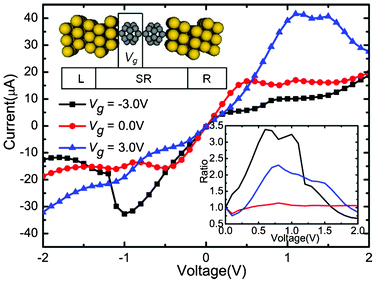 | ||
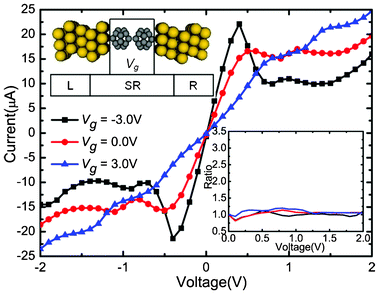
| Fig. 1 Calculated currents as a function of the applied bias under the Vg = −3.0, 0.0, and 3.0 V, respectively. Upper inset: Schematic description of the device: (C20)2 molecules sandwiched between Au electrodes. An additional Vg is applied asymmetrically on the left C20 molecule. The lower right inset shows the change of corresponding rectification ratio against the bias. | ||
3 Results and discussion
The self-consistently calculated I–V characteristics are shown in Fig. 1. Vg is set to three different values (−3.0, 0.0, and 3.0 V), and Vb is in a range from −2.0 to 2.0 V. This molecular junction demonstrates controllable gate–voltage dependence. The I–V curves show obvious asymmetry and nonlinear characteristics. No matter whether in positive or negative Vb regions, when Vb is low, currents increase faster when Vg is zero than when Vg is −3.0 V and 3.0 V . It seems that the transport abilities are suppressed by Vg. As the negative (positive) bias grows, the currents change quickly as the bias changes when Vg = −3.0 V (3.0 V). For the positive (negative) bias, the current values increase slowly and are obvious small. Thus, the devices show significant rectifying performances under the Vg. Moreover, negative differential resistance (NDR) behaviors are observed when Vg = 3.0 V, Vb = 1.0 V and Vg = −3.0 V, Vb = −1.0 V. In order to evaluate the rectification effect under different values of Vg, we calculated the rectification ratio, which is the ratio of currents between the absolute value under negative (positive) and positive (negative), when Vg = −3.0 V (3.0 V). The rectification ratio is shown in the lower right inset of Fig. 1. An I![[thin space (1/6-em)]](https://www.rsc.org/images/entities/char_2009.gif) +/I− ratio above 1 means a forward rectifying, while an I+/I− ratio above 1 means an inverse rectifying. From Fig. 1, we can clearly see that the gated I–V characteristics have distinct features compared with those of Vg = 0.0 V situation. When Vg = −3.0 V, the molecular device reveals a reverse rectifying, with a maximum ratio of 3.4 at 0.6 V. When Vg = 3.0 V, the molecular device reveals forward rectifying, with a maximum ratio of 2.3 at Vb = 0.8 V. Therefore, the application of asymmetric Vg can induce the rectification effect and the positive or negative value of Vg can significantly alter the rectifying direction.
+/I− ratio above 1 means a forward rectifying, while an I+/I− ratio above 1 means an inverse rectifying. From Fig. 1, we can clearly see that the gated I–V characteristics have distinct features compared with those of Vg = 0.0 V situation. When Vg = −3.0 V, the molecular device reveals a reverse rectifying, with a maximum ratio of 3.4 at 0.6 V. When Vg = 3.0 V, the molecular device reveals forward rectifying, with a maximum ratio of 2.3 at Vb = 0.8 V. Therefore, the application of asymmetric Vg can induce the rectification effect and the positive or negative value of Vg can significantly alter the rectifying direction.
The mechanisms of the changes in the electronic transport properties after applying Vg on the left C20 molecule can be interpreted in terms of the transmission spectra and the corresponding projection of the density of state (PDOS) at zero bias, and molecular projected self-consistent Hamiltonian (MPSH) of frontier molecular orbitals, as shown in Fig. 2. MPSH is the self-consistent Hamiltonian of the isolated molecule in the presence of the electrode, namely, the molecular part extracted from the whole self-consistent Hamiltonian. If an orbital is delocalized across the molecule, an electron that enters the molecule at the energy of the orbital has a high probability of reaching the other end, and thus there is a corresponding peak in the T(E). From Fig. 2, one can clearly see the gated modulation on molecular orbitals. A positive or negative Vg will, respectively, raise or lower the orbital energies in the molecules relative to the Fermi level (Ef). The transmission coefficients at Ef are 0.403, 0.555, 0.351 for Vg = −3.0, 0.0, 3.0 V, respectively. It is notable that when Vg = −3.0 V, LUMO+2 and LUMO+3 are close to Ef, and therefore LUMO+2 and LUMO+3 are the main transmission channels. When Vg = 0.0 V and 3.0 V, the LUMO and LUMO+1 resonances are close to Ef, and therefore LUMO and LUMO+1 are the main transmission channels. From Fig. 2(b), one can see that, LUMO and LUMO+1 for Vg = 0.0 V are delocalized, which result in the big current in the low Vb region. While LUMO+1 and LUMO+2 for Vg = −3.0 V, and LUMO and LUMO+1 for Vg = 3.0 V localize mainly at one side of (C20)2 molecules, which reduces the molecular conduction. In addition, the transmission coefficients of gated devices are all lower than those under Vg = 0.0 V at Ef, leading to the suppressed I–V curves at low bias in Fig. 1.
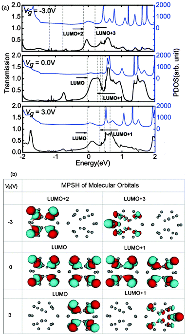 | ||
| Fig. 2 (a)Transmission spectra T(E) and corresponding PDOS at Vb = 0.0 V for different Vg. The dashed vertical lines stand for the molecular orbitals. The Fermi level Ef is set to zero. (b) MPSH of frontier molecular orbitals for different Vg values at Vb = 0.0 V. | ||
Another attractive phenomenon is the presence of rectifying behaviors in the gated I–V curves. In order to explain the origin of the rectification phenomenon, we plot the total transmission coefficients as a function of Vb under Vg = −3.0 V (Fig. 3(a)) and 3.0 V (Fig. 3(b)), respectively. As explained above, Vg can shift the transmission peak and make the transmission coefficients distribute asymmetrically. Fig. 3 shows that the transmission peaks shift to the positive energy direction. When Vg = −3.0 (3.0) V, as shown in Fig. 3(a) and (b), the transmission spectra within the bias window under negative (positive) bias are apparently stronger than those under positive (negative) bias, and therefore the current increases faster under negative (positive) bias than positive (negative) bias, showing evidently reversed (forward) rectification. When Vb increases to −0.6 (0.8) V, the difference of the current between the two bias regions reaches the maximum. Therefore, the rectification ratio can be up to its extreme value. However, another transmission peak appears in the positive (negative) energy region, which leads to a decrease of the difference of the current between the two bias regions and the decrease of the rectification ratio. When Vg = −3.0 (3.0) V, under the negative bias (positive) region, the transmission peaks decrease at bias of less (greater) than −1.0 (1.0) V, and this is responsible for the current drop from Vb = −1.0 (1.0) V. Consequently, the NDR peak appears.
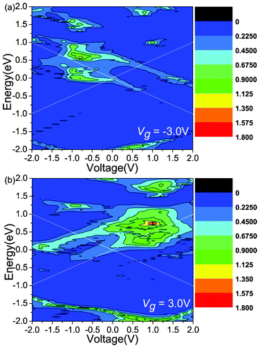 | ||
| Fig. 3 The total transmission coefficients as a function of the Vb under the Vg = −3.0 and 3.0 V, respectively. The white solid lines indicate the bias windows. | ||
As demonstrated by many investigations,28,29 the electronic transport properties of molecular wires are strongly dependent on the spatial distribution of the molecular orbitals. One of the key factors affecting the molecular rectification is the asymmetric shift of frontier orbitals under bias.28 As an effort to deeply understand the origin of the positive and negative rectification, we choose the transmission spectra of Vb = −1.0, 1.0 V under Vg = −3.0, 3.0 V and calculate the MPSH to explore the origin of the asymmetric transmission spectra with respect to bias. In the transmission spectra, the position of the transmission peak is generally determined by the energy level of molecular orbital, i. e. the transmission channels, and the delocalization of orbitals affects the height of transmission peak. The isosurfaces of MPSH eigenstates within the bias window for junction of Vg = −3.0 V at Vb = −1.0 and 1.0 V are plotted in parts (a) and (b) of Fig. 4, respectively. In the transmission spectrum of Vb = −1.0 V, there are five molecular orbitals (LUMO+2, LUMO+3, LUMO+4, LUMO+5 and LUMO+6) inside the bias windows. Two (LUMO+2 and LUMO+3) of the five molecular orbitals are spatially delocalized throughout the scattering region, resulting in the big and wide peaks in the transmission spectrum. Therefore, the peaks in the bias window have large contribution to the current. Because the molecular orbitals shift with the applied bias, the transmission spectra show clear bias-dependent. In contrast, at Vb = 1.0 V, the molecular orbitals LUMO+2 and LUMO+6 shift out of the bias windows and there are only three molecular orbital (LUMO+3, LUMO+4 and LUMO+5) inside the bias windows. All of the three molecular orbitals (LUMO+3, LUMO+4 and LUMO+5) are localized in the left C20 region, making a small contribution to the transmission spectrum featured by the small peaks. As a result, the current at Vb = −1.0 V is much higher than that at Vb = 1.0 V. This difference accounts for the negative rectifying properties of the molecular junction of Vg = −3.0 V. The isosurfaces of the MPSH eigenstates within the bias window for junction of Vg = 3.0 V at Vb = −1.0 and 1.0 V are plotted in parts (c) and (d) of Fig. 4, respectively. At Vb = −1.0 V, all the five molecular orbitals (HOMO, LUMO, LUMO+1, LUMO+2 and LUMO+3) inside the bias window are localized in either the left C20 region or the right C20 region. By contrast, two (LUMO and LUMO+1) of the three molecular orbitals inside the bias window at Vb = 1.0 V are delocalized throughout the scattering region, causing the big and wide peaks in the transmission spectrum. As a result, the molecular junction of Vg = 3.0 V shows a positive rectification behavior. The origin of the rectification properties can be understood from the position and intensities of molecular orbitals inside the bias window. We can infer that the Vb and Vg can shift the molecular orbitals and affect the coupling degree between the molecular orbitals and electrodes, which results in the rectification behaviors.
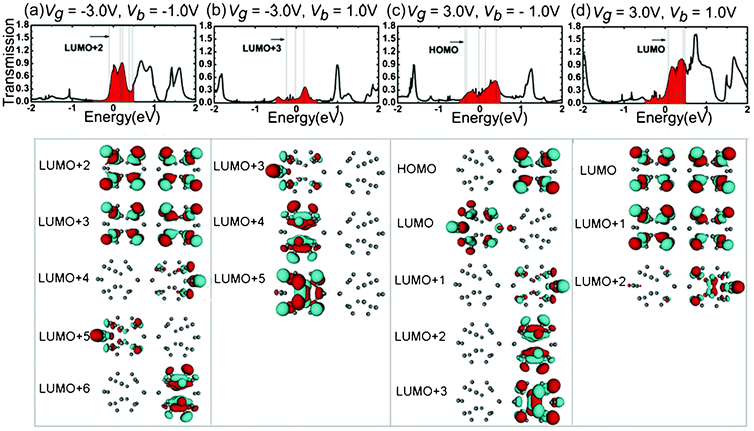 | ||
| Fig. 4 Transmission spectra (top panel) and isosurfaces (lower panels) of the MPSH eigenstates within the bias window from Ef = −0.5 to 0.5 eV. (a) and (b) for Vg = −3.0 V, (c) and (d) the Vg = 3.0 V. | ||
A concern of gated molecular junctions is whether the rectification behavior depends on different positions of the gate voltage. To address this issue, we calculated the I–V curves in a bias range from −2.0 to 2.0 V under Vg = −3.0, 0.0, and 3.0 V, which are applied on the whole (C20)2 molecules, The calculated I–V characteristics are shown in Fig. 5. The device does not exhibit the rectification behavior. Therefore, we can conclude that the different positions of Vg can affect the electronic transport properties. The rectification behavior can be induced by applying the Vg under one of the (C20)2 molecules and the rectification directions can be changed by the positive or negative value of the gate voltage.
 | ||
| Fig. 5 Calculated currents as a function of the applied bias under the Vg = −3.0, 0.0, 3.0 V, respectively. Upper inset: Schematic description of the device: (C20)2 molecules sandwiched between Au electrodes. An additional Vg is applied on the (C20)2 molecules. | ||
4 Conclusion
In summary, we performed a first-principle calculation on the electronic transport properties of a gated (C20)2 based molecular device. Rectification behaviors are found and the rectification directions can be modulated by the positive or negative value of Vg, originated from the asymmetrical shift of molecular orbitals. This rectification is fully rationalized by the calculated transmission spectra and the spatial distribution of the corresponding molecular orbitals. We proposed a new method for designing the molecular rectification device by using different applying positions of gate voltage. The finding can be useful for the development of future nanoelectronic devices.Acknowledgements
This work was supported by the National Basic Research Program of China (Grant No. 2009CB929204), Natural Science Foundation of China (Grant No. 11074146), the Ph.D. Programs Foundation of Ministry of Education of China (Grant No. 200804220005), the Natural Science Foundation of Shandong Province (Grant Nos. ZR2010AM026 and ZR2010AM037), and the Independent Innovation Foundation of Shandong University (Grant No. 2009TS097 and 2012TS025).References
- H. Park, J. Park, A. K. L. Lim, E. H. Anderson, A. P. Alivisatos and P. L. McEuen, Nature, 2000, 407, 57 CrossRef.
- A. N. Pasupathy, J. Park, C. Chang, A. V. Soldatov, S. Lebedkin, R. C. Bialczak, J. E. Grose, L. A. K. Donev, J. P. Sethna, D. C. Ralph and P. L. McEuen, Nano Lett., 2005, 5, 203 CrossRef CAS.
- C. G. Zeng, H. Q. Wang, B. Wang, J. L. Yang and J. G. Hou, Appl. Phys. Lett., 2000, 77, 3595 CrossRef CAS.
- J. Zhao, C. G. Zeng, X. Cheng, K. D. Wang, G. W. Wang, J. L. Yang, J. G. Hou and Q. S. Zhu, Phys. Rev. Lett., 2000, 95, 045502 Search PubMed.
- S. Nakanishi and M. Tsukada, Phys. Rev. Lett., 2001, 87, 126801 Search PubMed.
- M. Otani, T. Ono and K. Hirose, Phys. Rev. B: Condens. Matter Mater. Phys., 2004, 69, 121408 Search PubMed.
- J. J. Palacios, A. J. Prez-Jimnez, E. Louis and J. A. Vergs, Phys. Rev. B: Condens. Matter, 2001, 64, 115411 CrossRef.
- T. Yamamoto, K. Watanabe and S. Watanabe, Phys. Rev. Lett., 2005, 95, 065501 Search PubMed.
- F. Jiang, Y. X. Zhou, H. Chen, R. Note, H. Mizuseki and Y. Kawazoe, J. Chem. Phys., 2006, 125, 084710 Search PubMed.
- Z. Q. Fan, K. Q. Chen, Q. Wan, B. S. Zou, W. H. Duan and Z. Shuai, Appl. Phys. Lett., 2009, 92, 263304 Search PubMed.
- C. Roland, B. Larade, J. Taylor and H. Guo, Phys. Rev. B: Condens. Matter, 2001, 65, 041401 Search PubMed.
- R. Gutierrez, G. Fagas, G. Cuniberti, F. Grossmann, R. Schmidt and K. Richter, Phys. Rev. B: Condens. Matter, 2002, 65, 113410 Search PubMed.
- M. Otani, T. Ono and K. Hirose, Phys. Rev. B: Condens. Matter Mater. Phys., 2004, 69, 121408 Search PubMed.
- T. Yamamoto, K. Watanabe and S. Watanabe, Phys. Rev. Lett., 2005, 95, 065501 Search PubMed.
- Y. P. An, C. L. Yang, M. S. Wang, X. G. Ma and D. H. Wang, J. Chem. Phys., 2009, 131, 024311 Search PubMed.
- C. B. Winkelmann, N. Roch, W. Wernsdorfer, V. Bouchiat and F. Balestro, Nat. Phys., 2009, 5, 876 CrossRef CAS.
- T. P. I. Saragia and J. Salbeck, Appl. Phys. Lett., 2006, 89, 253516 Search PubMed.
- T. D. Anthopoulos, B. Singh, N. Marjanovic, N. S. Sariciftci, A. M. Ramil, H. Sitter, M. Colle and D. M. D. Leeuw, Appl. Phys. Lett., 2006, 89, 213504 CrossRef.
- A. R. Champagne, A. N. Pasupathy and D. C. Ralph, Nano Lett., 2005, 5, 305 CrossRef CAS.
- J. Taylor, H. Guo and J. Wang, Phys. Rev. B: Condens. Matter, 2001, 63, 121104 CrossRef.
- A. Saffarzadeh, J. Appl. Phys., 2008, 103, 083705 Search PubMed.
- A. A. Shokri and S. Nikzad, J. Appl. Phys., 2011, 110, 024303 Search PubMed.
- Z. Q. Fan and K. Q. Chen, J. Appl. Phys., 2011, 109, 124505 CrossRef.
- S. J. Wind, J. Appenzeller and P. Avouris, Phys. Rev. Lett., 2003, 91, 058301 CrossRef CAS.
- See http://www.quantumwise.com/for for more information about Atomistix ToolKit.
- J. Taylor, H. Guo and J. Wang, Phys. Rev. B: Condens. Matter Mater. Phys., 2001, 63, 245407 CrossRef.
- M. Brandbyge, J. L. Mozos, P. Ordejon, J. Taylor and K. Stoll, Phys. Rev. B: Condens. Matter Mater. Phys., 2002, 65, 165401 CrossRef.
- Y. Xing, L. Hongmei and Z. Jianwei, J. Chem. Phys., 2006, 125, 094711 CrossRef.
- A. Staykov, D. Nozaki and K. Yoshizawa, J. Phys. Chem. C, 2007, 111, 11698.
| This journal is © The Royal Society of Chemistry 2012 |