Hybrid 3D graphene and aligned carbon nanofiber array architectures†
Gui-Ping
Dai
a,
Marvin H.
Wu
b,
Darlene K.
Taylor
a,
M. Kyle
Brennaman
c and
K.
Vinodgopal
*a
aDept. of Chemistry, North Carolina Central University, Durham, NC 27707, USA. E-mail: kvinodg@nccu.edu
bDept. of Physics, North Carolina Central University, Durham, NC 27707, USA
cDept. of Chemistry, University of North Carolina at Chapel Hill, Chapel Hill, NC 27599, USA
First published on 14th August 2012
Abstract
We report a one-step, low-pressure, chemical vapor deposition (CVD) process to obtain a three-dimensional (3D) carbon architecture consisting of vertically aligned carbon nanofiber arrays on multi-layered graphene films. The morphology and structure of the hybrid materials grown on transmission electron microscopy copper grids have been determined by electron microscopy and Raman spectroscopy.
Integration of 2D graphene and 1D carbon nanofibers (CNFs) or nanotubes (CNTs) into hybrid 3D architectures is a useful route to pursue for a variety of applications, particularly energy storage.1,2 Recent efforts at fabricating such hybrid architectures have involved different experimental approaches,3–11 ranging from spin-coating or self-assembly of homogeneously mixed solutions of reduced graphene oxide (rGO) and CNTs using surface-functionalization to multi-step combination methods of a solution process and CVD to yield 3D rGO/CNT/rGO sandwich structures. However, all of these methods require multi-step fabrication processes, where either Fe,7,10 Ni,8,11 or Si9 nanoparticles were used to catalyze growth of CNTs, and GO or rGO was used as the non-ideal substitute for graphene.3–5,8 Hence, it would be quite advantageous to construct such a 3D hybrid nano-architecture in a one-step process involving the simultaneous growth of graphene and CNTs or CNFs on a single metal substrate.
In this communication, we report the first successful direct synthesis of 3D graphene/CNFs nano-architecture in a low pressure CVD (LP-CVD) chamber, where both high-quality graphene films with 1–4 layers and a “forest” of vertical well-aligned CNF arrays grow simultaneously on copper TEM grids in a one-step process without any other metal or non-metal catalysts. The graphene/CNF-arrays were directly prepared by using a LP-CVD technique, consisting of a quartz tube furnace connected to a mechanical pump, a gas manifold for controlling the gas flow rate and composition, and a pressure manifold for controlling the reactor pressure. Details of the CVD process are provided in the ESI,† although the salient features are (1) a high flow rate, (2) higher ratio of methane to hydrogen and (3) pressures of 2.5 Torr. Commercially available copper grids (Electron Microscopy Sciences) were employed as substrates. The direct growth of the graphene/CNF hybrid architecture on TEM grids enables direct in situ examinations of as-synthesized aligned CNF arrays by a high-resolution TEM (HR-TEM). Samples were directly characterized by SEM (FEI NanoSEM 630), HRTEM (JEOL 2010F-FastTEM), and Raman spectroscopy (Reinshaw inVia) without any post-treatments.
Fig. 1 shows typical SEM images of the CNFs/graphene hybrid architecture on TEM grids. The well-aligned CNF arrays directly grow on the graphene surface. The low resolution SEM image (Fig. 1a) shows a grid crossbar overgrown with CNFs/graphene at high surface coverage. The bright features in the SEM image in Fig. 1a correspond to the CNF forests and the small dark regions are the bare graphene-covered Cu surfaces.
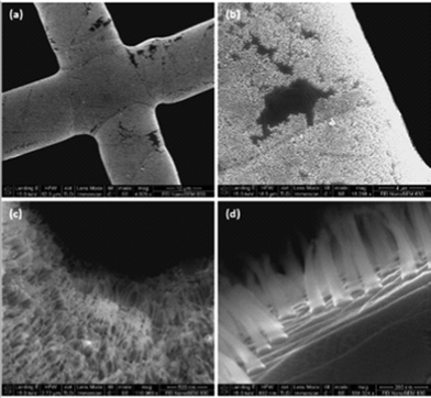 | ||
| Fig. 1 Typical SEM images of the as-prepared graphene/CNF-forest hybrid materials. (a–c) Low magnification. (d) High magnification. | ||
The dark region can be more clearly seen in Fig. 1b, which shows large Cu terraces covered in graphene sheets in several micrometer sizes, surrounded by dense CNF forests. Terraces or steps are features commonly found on the surface of annealed Cu.12 The enlarged view (Fig. 1c) reveals that the bright features are large and well-aligned CNF forests in the crossing edge of the Cu grid. At high magnification (Fig. 1d), individual CNFs and graphene films are clearly observed at the grid edge surfaces, while graphene sheets cross through grain boundaries and steps or terraces of Cu. The CNF forests have a uniform height of about 400 nm. Variations of carbon density in individual CNFs, indicated by the change of contrast in the SEM images (Fig. 1d), are observed. A typical CNF tapers upwards with a root diameter between 80–140 nm which decreases to 30–70 nm in the middle and tip of the CNF. The fact that the CNFs can be sharply imaged, without distortions, indicates that they are not electrically charged by the electron beam. This is consistent with the inherent high electrical conductivity of CNFs.13 The CNFs are quite pure without detectable metal nanoparticles, as confirmed by TEM. This is an important observation as it establishes a direct route to synthesis that does not involve the use of Fe, Co, or Ni, which have been typically used as catalysts for fabrication of 1D CNFs or CNTs.13 Additional top-down SEM images are presented in the ESI (Fig. S1 and S2).†
HRTEM images can provide detailed microstructural information on CNFs and direct evidence of the number of graphene layers. Fig. 2a–d show typically direct side and bottom-view TEM images of CNF arrays. Fig. 2a shows dense and vertical well-aligned CNF forests of uniform height growing on the edge surfaces of Cu grids. Fig. 2b shows that the interiors of CNFs consist of a large amount of amorphous carbon in the sp3 hybridization state, which is enclosed by a thin sp2 graphitic shell. The inset image of selected area electron diffraction (SAED) in Fig. 2d, showing an absence of six-fold-symmetrical spots, confirms the amorphous nature of the interior of the CNFs. However, the nature of the shells consisting of graphitic layers is clearly demonstrated in the HRTEM image shown in Fig. 2c. The root, consisting of much denser amorphous carbon (C core) compared to the tip, can be clearly seen in Fig. 2d. These C cores may act as nucleation sites to facilitate growth of CNFs. This will be clarified in the subsequent discussions.
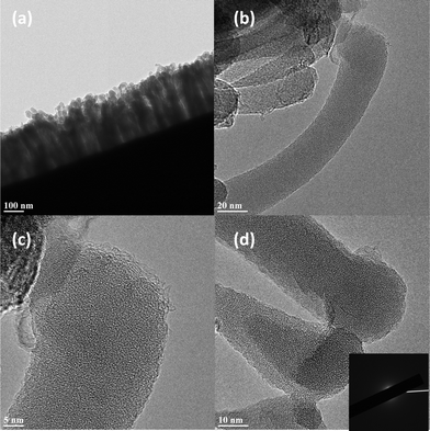 | ||
| Fig. 2 (a–b) Typical TEM images of CNFs. (c–d) HRTEM images showing the graphitic shell and amorphous interior. | ||
To characterize graphene sheets on the Cu surface, samples of the as-prepared graphene–CNF hybrids were sonicated in methanol for a few minutes, and the resulting solution was then drop cast on holey TEM grids for observation. HRTEM image (Fig. 3a) confirms that the Cu surface has single-layer, double-layer, and three-layer graphene sheets (as shown with blue, red, and purple arrowheads, respectively), and the upper thicker part is from lacey carbon on the TEM grid. The clear lattice fringes (as shown in Fig. 3b with white arrowheads) with 3–4 layers confirm the well-ordered crystalline structures and high quality of graphene sheets. Additional TEM characterizations including the electron diffraction patterns are show in the ESI (Fig. S4).†
 | ||
| Fig. 3 Typical HRTEM images of graphene films from Cu substrate after sonication treatment. (a) Blue, red, and purple arrowheads represent single-layer, double-layer, and triple-layer graphene sheets, respectively. (b) White arrowheads indicate the lattice fringes of graphene film. A magnified image is also shown in ESI, Fig. S3.† | ||
To confirm that the CNF forests grow directly on the graphene surface, we halted growth before forming CNF forests. Fig. 4a is a typical high-resolution SEM image of the Cu grid surface with enhanced contrast after CVD growth, showing the presence of many carbon cores (initial nucleation portions of CNFs), the presence of Cu surface steps, graphene wrinkles, and the presence of non-uniform dark flake-decorated graphene films. Graphene forms across Cu grain boundaries, indicating that the graphene film is continuous. Raman measurements performed at shorter deposition times under otherwise identical experimental conditions show that the Cu surfaces are nearly completely covered by graphene and are shown in the ESI (Fig. S5).†Fig. 4b is a typical SEM image of the Cu grid surface after sonication for a few minutes, showing the presence of non-uniform dark graphene flakes. This indicates that the graphene film is not completely removed from the Cu grid surface, but most of the CNF forests have been removed from the graphene surface after sonication.
 | ||
| Fig. 4 (a) Typical high-resolution SEM image showing carbon cores, a Cu grain boundary and steps, 1–4 layers of graphene flakes, and graphene wrinkles. (b) Typical SEM image of Cu surface showing residual graphene flakes after sonication. | ||
The observations demonstrate that CNF forests directly grow on the top surface of graphene films to form a seamless crystalline interface, which is comprised of typical C–C covalent bonds (π–π interactions) between two allotropes. This type of hybrid architecture with a direct contact enables various applications for these hybrid materials, especially in interconnects and field-emitting devices. Vertical, dense, and well-aligned CNF forests grown on planar graphene imply a large available surface for charge storage, thereby making these hybrid materials excellent candidates for application in energy storage devices such as high performance electrodes, supercapacitors and batteries.
To further evaluate the structure of the CNFs and verify the thickness and quality of graphene films, Raman spectra were obtained at an excitation wavelength of 632.8 nm. Fig. 5 shows typical Raman spectra recorded from different locations of the graphene/CNF-forest hybrid films. Fig. 5a is taken from an area rich in CNF forests, while the spectra in Fig. 5b are taken from graphene-rich regions. The Raman spectrum of CNF forests in Fig. 5a consists of two main peaks: D (1324 cm−1) and G (1591 cm−1), respectively. The G peak corresponds to E2g stretching mode of the graphitic crystalline structure. The D peak is due to the breathing modes of six-atom rings and requires a defect for its activation, i.e. the peak arises from lattice disorder.14
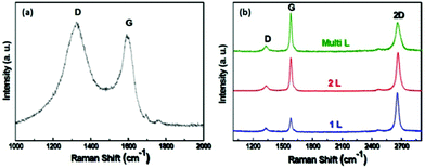 | ||
| Fig. 5 (a) Typical Raman spectrum of CNF forests with an excitation wavelength of 632.8 nm. (b) Typical Raman spectra showing single-, double-, and multi-layer graphene on graphene-rich regions of the Cu surface. | ||
The G-band for CNF shows a significant asymmetry at lower wavelengths, resulting from overlap with the higher D-band, giving additional evidence of imperfect structure. Overall, the Raman spectrum indicates that the CNF forests contain a large amount of sp3 amorphous carbon and a small number of sp2 crystallite portions, which is corroborated by HRTEM observations. The Raman spectra in Fig. 5b consist of a set of distinct peaks that are similar to those of graphene films grown on Cu foils previously reported by Li et al.12 The weak defect-related D-peak at 1326 cm−1 may arise from wrinkles and domain boundaries, and the strong G-peak at 1581 cm−1 indicates excellent crystallinity of graphene films. In addition to G-band and D-band peaks, the 2D-band peak appearing at 2656 cm−1 is the most prominent feature in the Raman spectra of the underlying graphene, and its position and shape can be used to clearly distinguish between single-layer, double-layer, and multi-layer graphene.14 The blue spectrum in Fig. 5b shows a narrow line width (full width at half maximum, FWHM = ∼35 cm−1) with a single Lorentzian profile, which are hallmarks of the monolayer graphene.12,14 Furthermore, a 2D to G peak intensity ratio of 3.02 was observed in our sample, corresponding to monolayer graphene. The intensity ratio of 2D and G band peaks in the red spectrum of Fig. 5b is close to 1.16, representing the double-layer graphene. For the Raman spectrum of multi-layer graphene (green spectrum in Fig. 5b), the G band intensity is much stronger as compared to that of the 2D band peak. These characterizations are consistent with HRTEM observations, confirming that CNFs directly grow on the surface of graphene to form 3D graphene/CNF-forests architectures in our LP-CVD system. It is worth noting that, although TEM Cu grid is the only substrate in the discussion, the graphene/CNF-forests can be made on Cu foils for arbitrarily large areas, limited only by the sizes of the CVD reactors and the copper substrates used for film deposition.
It is well known that graphene growth on copper is a surface-mediated process.12 However, it is somewhat surprising that CNFs can grow on the surface of graphene/copper without any other metal particles. HRTEM and SEM images reveal that there are no encapsulated catalytic metal nanoparticles at the walls and tips of the CNFs. Each CNF has a varying density, where the root consists of more dense amorphous carbon compared to the bulk. From this microscopic evidence, we construct a probable formation scenario for CNFs according to a base-growth mode. Copper is generally not considered an active catalyst for the growth of CNFs. However, a common feature of CVD synthesis of graphene is formation of a large amount of Cu nanoparticles on the surface at high temperatures (typically 1035 °C) during the reactor temperature ramp and copper annealing steps. These nanoparticles may act as the original centers for nucleation of graphene flakes.12 The morphology of the copper surface, such as roughness, steps, terraces, grain boundary, and defects, plays a crucial role in forming nucleation seeds of graphene.15 Nearly full coverage of copper surface with graphene can be achieved within seconds. This growth rate is higher than previous results reported in literature, but this is a factor of both the higher ratio of methane to hydrogen (75%) and the relatively higher reaction pressure (2.5 Torr) used herein. Due to the self-limiting growth conditions of graphene,12 excessive or supersaturated carbon species adsorb, dissolve, diffuse, and precipitate to form carbon structures on active sites in the Cu surface (steps, terraces, grain boundary, defects, and nanoparticles). These sites remain active although covered by an atom-layer thickness of graphene, which results in the formation of C cores following a base-growth mode and the CNFs grow in a self-assembled fashion.
In summary, we wish to emphasize that this is the first time that such a novel 3D hybrid composed of graphene/CNF-forests, has been experimentally synthesized by a one-step process.
We wish to thank NSF CREST award HRD-0833184 for financial support of this research (K.V., D.K.T., and M.H.W.). Grant DMR-0959679 provided support for SEM images. Partial funding for M.H.W. was provided by NASA URC award NNX09AV07A. M.K.B. is supported as part of the UNC EFRC: Center for Solar Fuels, an Energy Frontier Research Center funded by the U.S. Department of Energy (Award Number DE-SC0001011). The assistance of Dr A. S. Kumbhar (HR-TEM measurements), Nanofabrication Laboratory, University of North Carolina at Chapel Hill, is also greatly appreciated.
References
- G. K. Dimitrakakis, E. Tylianakis and G. E. Froudakis, Nano Lett., 2008, 8, 3166–3170 CrossRef CAS.
- S. Paulson, A. Helser, M. B. Nardelli, R. M. Taylor, M. Falvo, R. Superfine and S. Washburn, Science, 2000, 290, 1742–1744 CrossRef CAS.
- D. H. Lee, J. E. Kim, T. H. Han, J. W. Hwang, S. Jeon, S. Y. Choi, S. H. Hong, W. J. Lee, R. S. Ruoff and S. O. Kim, Adv. Mater., 2010, 22, 1–6 CrossRef.
- Z. J. Fan, J. Yan, L. J. Zhi, Q. Zhang, T. Wei, J. Feng, M. Zhang, W. Qian and F. Wei, Adv. Mater., 2010, 22, 3723–3728 CrossRef CAS.
- L. Peng, Y. Feng, P. Lv, D. Lei, Y. Shen, Y. Li and W. Feng, J. Phys. Chem. C, 2012, 116, 4970–4978 CAS.
- C. Y. Li, Z. Li, H. W. Zhu, K. L. Wang, J. Q. Wei, X. Li, P. Sun, H. Zhang and D. Wu, J. Phys. Chem. C, 2010, 114, 14008–14012 CAS.
- R. K. Paul, M. Ghazinejad, M. Penchev, J. Lin, M. Ozkan and C. S. Ozkan, Small, 2010, 6, 2309–2313 CrossRef CAS.
- Y. Ma, L. Sun, W. Huang, L. Zhang, J. Zhao, Q. Fan and W. Huang, J. Phys. Chem. C, 2011, 115, 24592–24597 CAS.
- X. Dong, B. Li, A. Wei, X. Cao, M. B. Chan-Park, H. Zhang, L. J. Li, W. Huang and P. Chen, Carbon, 2011, 49, 2944–2949 CrossRef CAS.
- D. D. Nguyen, N. H. Tai, S. Y. Chen and Y. L.Chueh, Nanoscale, 2012, 4, 632–638 RSC.
- Y. S. Kim, K. Kumar, F. T. Fisher and E. H. Yang, Nanotechnology, 2012, 23, 015301–015307 CrossRef.
- X. Li, W. Cai, J. An, S. Kim, J. Nah, D. Yang, R. Piner, A. Velamakanni, I. Jung, E. Tutuc, S. K. Banerjee, L. Colombo and R. S. Ruoff, Science, 2009, 324, 1312–1314 CrossRef CAS.
- R. H. Baughman, A. A. Zakhidov and W. A. de Heer, Science, 2002, 297, 787–792 CrossRef CAS.
- L. G. Cancado, A. Jorio, E. H. Martins Ferreira, F. Stavale, C. A. Achete, R. B. Capaz, M. V. O. Moutinho, A. Lombardo, T. S. Kulmala and A. C. Ferrari, Nano Lett., 2011, 11, 3190–3196 CrossRef CAS.
- G. H. Han, F. Gunes, J. J. Bae, E. S. Kim, S. J. Chae, H. J. Shin, J. Y. Choi, D. Pribat and Y. H. Lee, Nano Lett., 2011, 11, 4144–4148 CrossRef CAS.
Footnote |
| † Electronic Supplementary Information (ESI) available. See DOI: 10.1039/c2ra21084c |
| This journal is © The Royal Society of Chemistry 2012 |