New possibilities for soft matter applications: eliminating technically induced thermal stress during FIB processing†
Roland
Schmied
a,
Boril
Chernev
a,
Gregor
Trimmel
b and
Harald
Plank
*ac
aCenter for Electron Microscopy, Steyrergasse 17, 8010 Graz, Austria.. Tel: +43 316 873 8324
bInstitute for Chemistry and Technology of Materials, Graz University of Technology, Stremayrgasse 9, 8010 Graz, Austria. Tel: +43 316 873 32281
cInstitute for Electron Microscopy and Fine Structure Research, Graz University of Technology, Steyrergasse 17, 8010 Graz, Austria. E-mail: harald.plank@felmi-zfe.at; Tel: +43 316 873 8821
First published on 13th June 2012
Abstract
Heating effects on focused ion beam processing have been identified as a strong convolution of intrinsic and technically induced contributions via experiments and simulations. The systematic parameter variation reveals that classic serpentine- or raster-like patterning strategies can imply an additional heating of more than one order of magnitude above the intrinsic temperature increase during single ion beam pulses. This rise in temperature can lead to severe chemical damage of materials with a low melting point, such as polymers or biological samples. Based on these findings, an alternative patterning sequence is introduced which is able to eliminate this technically induced heating whereas process times are not affected. It is shown that chemical damage of the (polypropylene) test polymers is strongly reduced and can be compared to the results after classic FIB processing with low ion beam currents (500 pA → 50 pA, 30 kV primary energy) or at cryogenic sample temperatures (−150 °C). The successful reduction of local thermal stress towards the intrinsic and unavoidable limit – related to single pulse effects – might open new possibilities for focused ion beam processing of soft matter.
Introduction
Over the last few decades focused ion beam (FIB) processing has attracted enormous attention, not only due to its unique capabilities as a site-specific lamella preparation tool for transmission electron microscopy, but also as a method for 3D metrology and 3D surface structuring from the micro- to the nano-scale.1,2,3 Because of its flexibility and its rapid implementation, it is of particular importance for prototyping applications in science and technology.3,4,5,6,7,8 Besides the undoubted advantages of FIB processing there are problems, however, such as spatially confined ion implantation,1,2 surface amorphization2,9,10 and partial high thermal stress.5,11,12 While the former two are intrinsic properties and therefore invariable, local heating effects can considerably alter or damage sensitive samples such as nano-scale devices, thin films, or materials with a low melting point such as polymers and biological material.11,13,14,15 One way of reducing thermal stress is by applying low temperature stages (down to liquid nitrogen temperatures), as was impressively demonstrated for polymers, compound materials and biological samples.12,16,17,18,19,20 A more straightforward strategy of reducing thermal stress is by carefully adapting process parameters, primarily via low ion beam currents and short beam dwell times on the microsecond scale or below, as Giannuzi et al.1 successfully proved. Kim et al. used thin films of a PS-b-PMMA block copolymer21 to demonstrate that chemical damage upon ion beam related heating is clearly dose dependent and can almost be eliminated by low ion beam currents and low sample temperatures of −100 °C. To our knowledge, Kim et al.'s study was the first one to reveal that even soft matter can be processed via focused ion beams with a minimum of chemical damage related to intrinsic effects on individual ion-material events. Very recently, Bassim et al. investigated the influence of a variety of FIB process parameters on the chemical damage of polyacrylamide films.22 Their results showed that, besides the reduction of the ion beam current, an increase of the point-to-point distance of consecutive patterning points can also reduce chemical damage. This influence had already been reported in literature before by several other authors,23,24,25 but only a few studies focused on different patterning sequences.26In this study we initially vary the most important FIB process parameters and identify a technically induced heating effect for standard patterning sequences, which massively damages the used test polymers. Based on our findings we then introduce an alternative patterning strategy which eliminates any unwanted additional heating and reveals a performance at room temperature which is comparable to the results obtained via standard patterning on cryogenic sample temperatures.
Results and discussion
Regular patterning for focused ion beam (FIB) related milling processes is typically realized by serpentine- or raster-like sequences of consecutive discrete points with a beam dwell time tDT and a point pitch (PoP) distance dPoP. As a starting point, the removal rate (RR) was investigated for different types of poly-propylene (PP) polymers (see Table 1) according to dwell times for various ion beam currents and sample temperatures. In order to ensure comparability, identical patterning footprints of 4 × 4 μm2 with default PoP values of 20 nm (related to 500 pA beam current) were used while total ion doses were kept constant via decreasing patterning loop numbers for increasing dwell times. To account for redeposition influences,7,27,28,29 the milling depths and side wall angles were investigated depending on the relevant ion doses and revealed a linear behavior (see Fig. S1†) which indicates a minor influence of material redeposition26 on the used patterning design and the applied ion doses. As illustrated by the squares in Fig. 1a, for a comparable high ion beam current of 500 pA (30 kV), the RR for regular patterning at room temperature is mostly constant at 50 ± 5 nm s−1 up to a dwell time of about 200 μs, followed by a strong increase. The inset in Fig. 1a shows a representative atomic force microscopy (AFM) height image of a structured PP surface processed with 500 pA, 20 nm PoP, and 1 μs dwell time at room temperature via regular patterning. Lowering the sample temperature to −150 °C while keeping other parameters constant reveals a very similar RR behavior; however, it shows a shifted RR increase for dwell times above ∼400 μs (triangles). Low current experiments with 50 pA (30 kV) at room temperature (circles in Fig. 1a) reveal a qualitatively similar behavior, but have reduced RR values (see right y-axis) and a shifted increase for dwell times of above ∼500 μs for regular patterning strategies. Fig. 1b gives a RR comparison for different PP types according to Table 1, processed via 500 pA and 20 nm PoP at room temperature via regular patterning strategies. After a widely constant RR for short dwell times (see upper inset in Fig. 1b), the onset of the RR increase is shifted to shorter dwell times for shorter polymers, which is found to scale linearly with the polymers molecular weight, as representatively shown for measurements of 660 μs and 1000 μs dwell time in the lower inset of Fig. 1b. | ||
| Fig. 1 (a) Removal rate vs. beam dwell time for 500 pA regular (squares), 50 pA regular (circles, right axis) and 500 pA interlace (stars) patterning at room temperature in comparison to −150 °C experiments for 500 pA regular (triangles) and 500 pA interlace (diamonds) strategies at constant ion doses, point pitches and pattern dimensions for PP-1. The inset shows an AFM height image for regular patterning with 500 pA at room temperature; (b) removal rate behavior for PP-1 (squares), PP-2 (circles), and PP-3 (triangles) structured with 500 pA at room temperature through regular patterning. The insets show the results on a logarithmic dwell time scale (top) and for representative removal rate values for 660 μs (solid) and 1000 μs (dashed) dwell time as a function of the molecular weight, revealing a linear scaling (bottom). All experiments were performed using a primary ion energy of 30 kV. | ||
| MFI/g per 10 min | M N/g mol−1 | T M/°C | ||
|---|---|---|---|---|
| PP-1 | 0.35 | 148000 | 164.2 |

|
| PP-2 | 2.44 | 85500 | 165.4 | |
| PP-3 | 19.57 | 52000 | 165.7 |
In order to investigate the thermodynamic behavior of the used PPs, differential scanning calorimetry was used as shown by the solid line in Fig. 2 for PP-1. The melting range spans from ∼150 °C to ∼175 °C and has its peak at ∼165 °C; this is found to be similar in all the investigated PP types (see Table 1). Further heating of the material leads to an endothermic chemical degradation (thermal pyrolysis) by the break-up of the weakest carbon–carbon links of the methyl groups and/or the polymer backbone, which reduces progressively its effective polymer length (molecular weight).30 Polymer fragments with less than about 20–30 carbons31 are capable of leaving the solid; this phenomenon is called the volatizing threshold and can be found experimentally at ∼325 °C via thermogravimetric analysis, as is representatively shown for PP-1 by the dashed curve in Fig. 2.
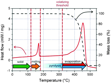 | ||
| Fig. 2 Differential scanning calorimetry (solid line, left axis) and thermogravimetric analysis (dashed line, right axis) measurements, representatively shown for PP-1. They are practically identical for all PP types used in this study. | ||
While Fig. 1 shows the RR as a function of the dwell time with 20 nm PoP, Fig. 3 shows the RR behavior for increasing PoP values at room temperature (squares): for dwell times of 500 μs (top) and 50 μs (center) the RR decreases and approaches a constant value of about 50 ± 5 nm s−1 at PoP values of above ∼70 nm and ∼30 nm, respectively. Short dwell times of 5 μs (bottom) reveal mainly constant RR values, similar to the saturation value for higher dwell times (top and center). As found for the dwell time experiments in Fig. 1, even low sample temperatures of −150 °C cannot prevent the RR increase for small PoP values at 500 μs and 50 μs, which is illustrated by the circles in Fig. 3 (top and center). Further verification experiments with a second polymer (high-density polyethylene) to exclude a specific PP behaviour reveal very similar tendencies for dwell time (Fig. S2, top) and PoP experiments (Fig. S2, bottom).† The slightly different RR values are attributed to the different thermodynamic properties.
 | ||
| Fig. 3 PP-1 related removal rates as functions of PoP distances for 5 μs (bottom), 50 μs (center), and 500 μs (top) dwell time at room temperature (squares) and −150 °C (circles) via regular patterning at 30 kV/500 pA. The stars illustrate the interlacing strategy which results at room temperature with an interlacing point pitch of 100 nm. The top AFM images show 1 × 1 μm bottom areas of structured PP according to the parameters indicated (Z range is 15 nm); rms roughness has been found to 0.2, 2.9, and 0.3 nm for (1), (2), and (3), respectively. | ||
The RR increase for higher dwell times in Fig. 1 indicates an enhanced material removal and is suggested to be the result of local heating above the volatizing threshold. At the volatizing threshold the polymer fragments are short enough to be evaporated (see Fig. 2) due to increasing local temperature for longer single point exposure. Further evidence for this assumption comes from dwell time experiments on different PP types, as shown in Fig. 1b: the onset of the RR increase is shifted to higher dwell times for longer PP polymer chains (higher molecular weight) which require more time at high temperatures before individual fragments are short enough to be evaporated. The linear RR scaling vs. the molecular weight for constant dwell times, as representatively shown in the bottom inset in Fig. 1b, supports even further the interpretation of the RR increase as a result of thermally assisted evaporation due to local heating beyond the volatizing threshold. In order to reduce FIB related heating effects by improved heat dissipation, a variable temperature stage was used for identical investigations at −150 °C. The related dwell time results are shown by triangles in Fig. 1a and reveal a behavior qualitatively very similar to room temperature experiments, however, the RR onset shifts towards higher dwell times. This finding is essential as it indicates that even sample temperatures as low as −150 °C can only delay, but not prevent local heating above the volatizing threshold. This effect is caused mainly by the very low thermal conductivity of 0.22 W m−1 K−1 for PP30,31 which prevents a sufficiently fast heat removal from the beam related heating area. Furthermore, this implies that heating beyond the volatizing threshold is confined to the proximity of the ion beam, which corresponds to atomic force microscopy (AFM) height measurements (representatively shown in Fig. 1a), illustrating that the structure side walls are not completely molten, but still reveal the intended pattern geometry. If the strong temperature rise expanded to the micrometer scale, this would not be the case.
An alternative strategy of lowering thermal stress is by reducing the ion beam current. A lower ion beam current goes along with a reduced removal rate and thus causes additional drawbacks due to increased processing time. Even more, the circles in Fig. 1a show that even an ion beam current one order of magnitude lower cannot prevent the RR increase for dwell times above 500 μs. The circles also indicate that there is thermally assisted evaporation as a dominating proximity effect for regular patterning strategies – even for low beam currents and/or low stage temperatures.
In order to identify the nature of this proximity heating, a closer look at the patterning process is needed: during the first ion beam pulse (tDT) at the patterning point X1 the material heats up according to:12
 | (1) |
In this equation, ρ stands for material density, cp for specific heat, κ is thermal conductivity, and QX1 represents the amount of the induced heat by the ion beam. The resulting temperature increase after a single ion pulse with a given dwell time tDT at X1 is defined as “intrinsic heating” ΔTin. Subsequently, the ion beam is immediately shifted by the distance dPoP to patterning point X2 where the exposure process starts again. According to eqn (1), however, the temperature at patterning point X2 has already increased due to the previous event, hence changing the initial temperature for the second patterning point. Since the beam parameters are kept constant, the intrinsic temperature rise ΔTin has to be added to this remaining temperature, neglecting the temperature decay during the pulse in the first approximation. After completion of the second pulse, patterning point X2 shows a higher temperature than X1 did after the first pulse. As the patterning process continues, local temperatures at Xn can go up much higher than as is caused by intrinsic heating ΔTin, which leads to melting (at ∼165 °C), thermal pyrolysis, and eventually to thermally assisted evaporation after having exceeded the volatizing threshold of ∼325 °C.
Fig. 4a shows a spatially (vertical axis) and temporarily (horizontal axis) resolved simulation of the surface temperature (normalized to ΔTin) according to eqn (1) after one single ion beam pulse of 500 pA with a beam dwell time of 500 μs at point X1 (simulation details can be found in the Methodology section). As can be seen, the temperature in a PoP distance of 20 nm (default value) still has about 75% of its intrinsic temperature ΔTin (see indication) while a distance of e.g. 100 nm to X1 shows only 15% of the ΔTin. These findings are in well agreement with the findings by Bassim et al. and Brostow et al., which observed also less damage for increased point pitches.22,23
 | ||
| Fig. 4 (a) Finite element simulation of surface temperature evolution as a function of time (horizontal) and radial distance (vertical) after a single ion beam pulse. The double logarithmic plot is normalized to the initial temperature ΔTIN; (b) estimation of technically induced temperature increases during classic serpentine or raster strategies (normalized to the intrinsic temperature); (c) the saturation temperatures obtained in (b) vs. point pitch. | ||
Based on these simulations, the temperature increase of consecutive patterning points discussed above is simulated in Fig. 4b by sequentially adding an intrinsic heating ΔTin to the remaining temperature at subsequent points in a distance dPoP. The plot is referenced to the intrinsic heating ΔTin and reveals a high local temperature increase as the patterning continues along the scan direction. Fig. 4c shows the saturation temperatures as a function of the applied point pitch and suggests a temperature 20 times higher than ΔTin for 10 nm point pitches. These simulations support the hypothesis that the heat removal on the nano- and microscale happens much slower than the heat generation by the ion beam as a consequence of the low thermal conductivity which is a main difference compared to many inorganic materials where such technically induced heating effects are widely absent.1,2 Please note that this simulation represents an upper estimation of the unwanted temperature increase since the dynamic temperature decay of previous points is neglected in the first approximation; nevertheless, it reveals the massive impact of small point pitches on the final temperatures.
Based on these findings it can be stated that increasing point pitches reduce local thermal heating due to reduced starting temperatures of consecutive patterning points. To prove this hypothesis through an experiment, the PoP distance is gradually increased while patterning footprints and total ion doses are kept constant. As can be seen in Fig. 3, the RR (as a volatizing threshold indicator) strongly decreases for increasing point pitches, which confirms the above hypothesis that increasing PoP distances, according to eqn (1), entail a reduced starting temperature of X2. After a beam pulse duration of tDT, the final temperature at X2 is hence closer to the unavoidable intrinsic single pulse heating ΔTin. As a result, enhanced point pitches can prevent temperature increases related to patterning and also considerably reduce local thermal stress which is reflected by the absence of the volatizing threshold related RR increase. The experiments clearly demonstrate the convolution of intrinsic heating during a single beam pulse (unavoidable) and technically related heating by inappropriate patterning sequences; therefore, an alternative processing strategy is needed in order to reduce or even eliminate such technical implications. A straightforward adaptation by means of increased point pitches, however, is limited due to the unwanted increase of roughness of the milled bottom areas. This effect can be seen by the AFM height images (1) and (2) in Fig. 3 for 20 nm and 150 nm point pitch, respectively (Z-scale is 15 nm).
In order to compensate for this drawback, a multistep interlacing (IL) strategy was applied which Plank et al.32 had already successfully introduced before for similar processes. As shown in Fig. 5, the first step uses an interlace point pitch dIL large enough to prevent increased starting temperatures of consecutive patterning points (pattern is indicated by 1). After such an IL frame is finished, the entire pattern is shifted by a small value according to the desired point pitch dF (pattern is indicated by 2). The systematic shift of the pattern, according to the sequence in the bottom right frame in Fig. 5a thus allows for: (i) strongly reduced starting temperatures of consecutive patterning points within individual IL frames due to large point distances (vertical arrow in Fig. 4a); (ii) identical deposition times as via regular patterning; and (iii) the fabrication of very smooth surfaces due to small final point pitches. The latter effect can be seen by the AFM height image (3) in Fig. 3 for 100 nm interlacing and 20 nm final point pitch (Z-scale is 15 nm) which is found to be very similar compared to 20 nm point pitch via regular patterning sequences.
![(a) interlacing strategy scheme using a largely spaced pattern with the IL point pitch dIL which is then shifted by a small value dF (final sequence is shown in the bottom right frame); (b) PP-1 related removal rate vs. interlace point pitch dIL for constant pattern footprints and ion doses (top axes indicates the corresponding thermal relaxation time [TRT]) for 30 kV, 500 pA, 20 nm final point pitch dF, and 2000 μs dwell time.](/image/article/2012/RA/c2ra21025h/c2ra21025h-f5.gif) | ||
| Fig. 5 (a) interlacing strategy scheme using a largely spaced pattern with the IL point pitch dIL which is then shifted by a small value dF (final sequence is shown in the bottom right frame); (b) PP-1 related removal rate vs. interlace point pitch dIL for constant pattern footprints and ion doses (top axes indicates the corresponding thermal relaxation time [TRT]) for 30 kV, 500 pA, 20 nm final point pitch dF, and 2000 μs dwell time. | ||
Apart from these aspects, the interlacing strategy introduces a thermal relaxation time (TRT) for each single point given by the number of patterning points and their dwell times within the IL frame. This TRT is equivalent to a shift to the right in Fig. 4a and allows the material to cool down before the ion beam is placed within close distance (dF) during the following IL frame. Very large IL point pitches (dIL), however, lead to very short TRTs and, therefore, again to increased starting temperatures for subsequent IL patterning points. In order to demonstrate the mutual influence of interlace point pitch and TRT, Fig. 5b displays the RR as a function of the interlace point pitch dIL while dwell times, patterning footprints, final ion doses, and final point pitches dF are kept constant. As can be seen, there is a distinct minimum revealing the ideal interlacing PoP of about 100 nm for the used patterning footprint. Smaller dIL values are equivalent to the reduced downward shifts in Fig. 4a while larger dIL values are represented by a smaller shift to the right in Fig. 4a (reduced TRT). Both lead to unwanted temperature increases – although for different reasons. Please note the small plateau around 100 nm in (b) which indicates that the pattern itself is large enough to allow sufficient thermal relaxation of each single IL point, thus eliminating technically induced heating effects as observed for classic serpentine- or raster-scanning.
Pushing this principal even further, it is possible to (i) change the point sequence in order to maximize the distance of subsequent interlace points (see Fig. S3†) and to (ii) maximize the distance of subsequent points individually while simulating the in-plane temperature distribution; this latter one is subject of ongoing optimization and investigations.
In order to illustrate the performance of this IL strategy with a final point pitch dF of 20 nm and an ideal interlacing point pitch dIL of 100 nm, dwell time and PoP experiments were repeated at room temperature and at −150 °C (30 kV, 500 pA). Illustrated by the stars and diamonds in Fig. 1a, dwell time graphs do not show any tendencies for an increasing RR at room temperature or at −150 °C, respectively. This in particular demonstrates that IL patterning at room temperature can effectively prevent local heating above the volatizing threshold. It furthermore exhibits an even better performance compared to low temperature conditions with regular patterning. The same results are found for PoP sweeps with 5 μs, 50 μs, and 500 μs dwell time (illustrated by the stars in Fig. 3).
The absence of an RR increase only reveals, however, that the volatizing threshold is not passed via IL patterning. So far, no information about its influence on chemical degradation via thermal pyrolysis is available. Raman measurements were therefore performed for different preparation parameters, patterning strategies, and sample temperatures. As a quantitative measure for chemical PP degradation, the intensities of the CH2 and CH3 stretching vibration bands33 between 2700−1 cm and 3000−1 cm were integrated while imaging parameters were kept constant (see Fig. S4†). The results of these measurements are summarized in Fig. 6 and reveal that regular patterning massively degrades the polymer at increasing dwell times (shown by solid red bars). Surprisingly, lowering the sample temperature to −150 °C (right block) reveals only a slightly reduced – but nevertheless similar – degree of chemical degradation compared to room temperature (left block), which is a further indication that the maximum temperatures are confined to the proximity of the ion beam as a consequence of the inefficient heat removal due to the low thermal conductivities. In contrast to this, interlacing patterning (represented by green bars) strongly reduces chemical degradation and proves to be much more independent from dwell times, which correlates with the suggested mechanism of a technically induced temperature increase. The remaining weak damage increase for higher dwell times can be explained by increasing temperatures ΔTin during single pulses (intrinsic and unavoidable) also observed by Kim et al.7 The major discovery in this respect is the similar damage for interlacing strategies at room temperature compared to regular patterning at low temperatures, which strongly suggests that IL patterning can compensate for low temperature stages applied as a countermeasure for intense heating. This thought is supported further by a direct comparison of interlacing results for room and cryogenic temperatures which are found to be very similar (see Fig. 6). Finally, it is evident that a beam current reduction by one order of magnitude (illustrated by blue bars for 5 μs dwell time in Fig. 6) cannot reduce chemical degradation considerably but requires a process time 10 times higher, which might cause drift problems.
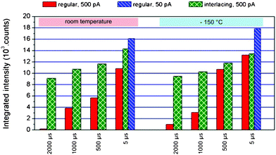 | ||
| Fig. 6 Raman summary for regular (red) and interlacing (green) patterning experiments at room temperature (left block) and −150 °C conditions (right block) for 500 pA, as well as for lower beam currents of 50 pA (blue). | ||
Experimental
Focused ion beam experiments were performed on a FEI NOVA 200 dual beam system. Ion beam energies were kept constant at 30 kV (Ga+) and structuring was performed in the eucentric height of 19.3 mm with ion beam currents of 500 pA and 50 pA. An in-house designed variable temperature stage was used for experiments at −150 °C (dynamic temperature control). To ensure reliability, the samples were kept on the stage for one hour after reaching the target temperature before focused ion beam structuring was started. An embedded scanning electron microscope was used for characterization of the removal rate by measuring the cross sections in tilted arrangements from different angles and the results were cross checked via AFM. Imaging parameters were set to 5 keV and 400 pA and pre-testing of the used polymers confirmed the absence of structural influences upon e-beam inspection. The internal NOVA 200 patterning engine was used for regular serpentine patterning strategies (default). Interlacing experiments used stream files which control the D/A patterning board directly and which were generated via C++ routines. To provide comparability for varying dwell time and point pitch experiments, the total exposure time and the total ion dose were kept constant via adapting the number of frame loops. 50 pA experiments were first referenced to identical milling depths for 500 pA using 1 μs dwell time, 20 nm point pitches and identical footprints. Three isotactic polypropylene polymers which differ in their molecular weights, as summarized in Table 1, were used for the experiments. Polymer bars with a cross section of 6x3 mm were precut and carefully polished to provide flat surfaces. Atomic force microscopy was used for reference depth measurements and it was performed with a Dimension 3100 microscope (Bruker AXS) with a Hybrid XYZ scan head and a Nanoscope IVa controller. Combined differential scanning calorimetry/thermogravimetric analysis measurements were performed with a Netzsch STA 449C (Netzsch Gerätebau GmbH) using a heating rate of 5 °C min−1 under a constant flow of helium (50.0 mL min−1). Raman spectra were measured using a Horiba Jobin Yvon LabRam 800 HR spectrometer with an Olympus BX41 microscope and a 633 nm He–Ne laser excitation with a 17 mW nominal power output. The used objective was Olympus MPlan N ×100 with NA 0.9. The slit width was 100 μm and the pinhole was closed to 200 μm. In order to avoid any damage caused the by laser beam, a ND 2.0 filter was used for the measurements. Comparability was ensured by performing all the measurements under identical conditions and by collecting the spectra within the region of 2500–3500 cm−1 at 3 x 150 s integration time. The integral intensities were calculated using the standard integration function of the supplied LabSpec® software. The spectral region between 2700 and 3000 cm−1, related to CH2 and CH3 stretching modes, was chosen as a measure for the remaining polypropylene. Integral intensities were calculated as the area above a linear background between the two border frequencies.Finite element simulations were performed with the software package ANSYS (V 13). The sample was modelled by an axisymmetric line with a length of 1 mm and a depth of 1 mm and later was meshed by the software's automatic meshing algorithm. In order to reveal the temporally resolved temperature distribution in a first approximation, a hemispherical volume according to the FWHM beam diameter of the ion beam (provided by the manufacturer [39 nm for 500 pA]) was heated up to a predefined target temperature according to the estimation by Volkert et al. and Kim et al.5,20 within a time according to the beam dwell time tDT. Thermal conductivity and specific heat capacity was assumed at 0.22 W m−1 K−1 and 2.5 kJ kg−1 K−1, respectively, in compliance with Khoury et al.30 Subsequently, the temporal and radial temperature distribution was normalized to the starting value in order to provide relative values instead of absolute temperatures, which are extremely complicated to verify through experiments. Varying the target temperature by one order of magnitude (250–2500 °C) only revealed very little variation of the relative results, however. A more sophisticated model – considering temperature dependent thermal conductivities/specific heat capacities, as well as Gaussian ion beam profiles instead of a circular area – which additionally uses SRIM simulation as input data, is currently being developed.
Conclusion
In this study we have investigated heating effects on polypropylene (representative soft matter) during focused ion beam processing. The systematic variation of dwell times and point pitches for different ion beam currents and sample temperatures reveals a nonlinear increase of the removal rate which is based on local heating effects beyond the volatizing threshold at which the material is thermally evaporated in the proximity of the ion beam. Correlated finite element simulations give strong evidence for a technically induced effect of classic serpentine- or raster-scans, based on increased temperatures of closely spaced consecutive points. This effect is caused by slow heat removal due to low thermal conductivities and can lead to local temperatures more than one order of magnitude higher than the intrinsic temperature rise of individual ion-material events. In order to allow for higher distances between consecutive patterning points and to minimize mutual heating influences, an alternative interlacing patterning strategy was introduced. Besides the successful reduction of local heating below the volatizing threshold, correlated Raman measurements confirm a reduced chemical damage at identical patterning times for interlacing procedures. Furthermore, we showed that applying interlacing strategies at room temperature delivers very similar results as regular patterning strategies at cryogenic sample temperatures. The absence of further improvements of interlacing procedures at cryogenic temperatures suggests strongly that this alternative patterning strategy can compensate for cryo-stages, which are applied as a countermeasure for massive heating. It is important to note, however, that the elimination of technically induced heating effects can only approach, but never prevent the intrinsic damage upon individual ion–matter events.Finally, it has to be stated that the implementation of interlacing strategies can be done entirely with the help of the accompanying standard software. This might open new possibilities for the combination of FIB processing and soft matter materials, which had been an unanswered question during the last few decades.
Acknowledgements
R. S., B. C. and H. P. gratefully acknowledge the valuable support provided by Prof. Ferdinand Hofer, Prof. Gerald Kothleitner, Dr Peter Willhelm and Dr Julian Wagner. The authors also thank FFG Austria and the Federal Ministry of Economy, Family and Youth of Austria for their financial support.References
- L. A. Giannuzi, F. A. Stevie, Introduction to Focused Ion Beams: Instrumentation, Theory, Techniques, and Practice. Springer, New York, USA, 2005 Search PubMed.
- J. Mayer, L. A. Giannuzi, T. Kamino and J. Michael, MRS Bull., 2007, 32, 400–407 CrossRef CAS.
- M. Y. Ali, W. Hung and F. Yongqi, Int. J. Precis. Eng. Manuf., 2010, 11(1), 157–170 CrossRef.
- R. M. Langford, M. Philipp, J. Gierak and Y. Q. Fu, MRS Bull., 2007, 32(5), 417–423 CrossRef CAS.
- C. A. Volkert and A. M. Minor, MRS Bull., 2007, 32(5), 389–399 CrossRef CAS.
- P. M. Nellen, V. Callegari and R. Bronnimann, Microelectron. Eng., 2006, 83(4–9), 1805–1808 CrossRef CAS.
- Y. K. Kim, A. J. Danner, J. J. Raftery and K. D. Choquette, IEEE J. Sel. Top. Quantum Electron., 2005, 11(6), 1292–1298 CrossRef CAS.
- T. Piok, H. Plank, G. Mauthner, S. Gamerith, C. Gadermaier, F. P. Wenzl, S. Patil, R. Montenegro, M. Bouguettaya, J. R. Reynolds, U. Scherf, K. Landfester and E. J. W. List, Jpn. J. Appl. Phys., 2005, 44(1B), 479–484 CrossRef CAS.
- J. P. McCaffrey, M. W. Phaneuf and L. D. Madsen, Ultramicroscopy, 2001, 87, 97–104 CrossRef CAS.
- L. Pastewka, R. Salzer, A. Gra, F. Altmann and M. Moseler, Nucl. Instrum. Methods Phys. Res., Sect. B, 2009, 267(18), 3072–3075 CrossRef CAS.
- N. Shukla, S. K. Tripathi, A. Banerjee, A. S. V. Ramana, N. S. Rajput and V. N. Kulkarni, Appl. Surf. Sci., 2009, 256(2), 475–479 CrossRef CAS.
- M. T. Myers, B. H. Sencer and L. Shao, Nucl. Instrum. Methods Phys. Res., Sect. B, 2012, 272, 165–168 CrossRef CAS.
- M. F. Hayles, D. J. Stokes, D. Phifer and K. C. Findlay, J. Microsc., 2007, 226(3), 263–269 CrossRef CAS.
- I. Brown, L. Yu, Z. Yu, Introduction to Ion Beam Biotechnology, Springer, New York, USA 2006 Search PubMed.
- P. K. Weber, J. Microsc., 2009, 238, 189–199 CrossRef.
- M. Marko, C. Hsieh, R. Schalek, J. Frank and C. Manella, Nat. Methods, 2007, 4, 215–217 CrossRef CAS.
- M. Marko, C. Hsieh, W. Moberlychan, C. A. Mannella and J. Frank, J. Microsc., 2006, 222, 42–47 CrossRef CAS.
- M. Sezen, Phys. Chem. Chem. Phys., 2011, 13(45), 20235–20240 RSC.
- M. Sezen, Phys. Chem. Chem. Phys., 2009, 11(25), 5130–5133 RSC.
- K. Niihara, Macromolecules, 2005, 38(8), 3048–3050 CrossRef CAS.
- S. Kim, M. J. Park, N. P. Balsara, G. Liu and A. M. Minor, Ultramicroscopy, 2011, 111, 191–199 CrossRef CAS.
- N. D. Bassim, J. Microsc., 2012 Search PubMed , in press.
- W. Brostow, B. P. Gorman and O. Olea-Mejia, Mater. Lett., 2007, 61, 1333–1336 CrossRef CAS.
- J. Orloff, M. Utlaut, L. Swanson, High Resolution Focused Ion Beams, Springer, New York, USA 2003 Search PubMed.
- J. J. Kochumalayil, Surf. Interface Anal., 2009, 41(5), 412–420 CrossRef CAS.
- W. C. L. Hopman, Nanotechnology, 2007, 18, 195305–195316 CrossRef.
- B. I. Prenitzer, C. A. Urbanik-Shannon, L. A. Giannuzzi, S. R. Brown, R. B. Irwin, T. L. Shofner and F. Stevie, Microsc. Microanal., 2003, 9, 216–236 CrossRef CAS.
- Y. Fu, N. K. A. Bryan, O. N. Shing and N. P. Hung, Int. J. Adv. Manuf. Technol., 2000, 16, 877–880 CrossRef.
- L. Frey, C. Lehrer and H. Ryssel, Appl. Phys. A: Mater. Sci. Process., 2003, 76, 1017–1023 CrossRef CAS.
- G. A. Khoury and B. Willoughby, Mag. Concr. Res., 2008, 60(2), 125–136 CrossRef CAS.
- J. D. Peterson, S. Vyazovkin and C. A. Wight, Macromol. Chem. Phys., 2001, 202(6), 775–784 CrossRef CAS.
- H. Plank, D. H. Smith, T. Haber, P. D. Rack and F. Hofer, ACS Nano, 2012 Search PubMed , in press.
- D. Lin-Vien, N. B. Colthup, W. G. Fateley, J. G. GrasselliThe Handbook of Infrared and Raman Characteristic Frequencies of Organic Molecules, Academic Press Inc., Boston, USA 191 Search PubMed.
Footnote |
| † Electronic supplementary information (ESI) available. See DOI: 10.1039/c2ra21025h |
| This journal is © The Royal Society of Chemistry 2012 |