DOI:
10.1039/C2RA20973J
(Paper)
RSC Adv., 2012,
2, 9590-9595
Improved electrical property of Sb-doped SnO2 nanonets as measured by contact and non-contact approaches
Received
17th May 2012
, Accepted 13th August 2012
First published on 14th August 2012
Abstract
This work reports the characterization of antimony doping effects on the electron transportation in SnO2 nanonets via a contact (field-effect transistor) and a non-contact (terahertz time-domain spectroscopy) approach. The doping influence is well demonstrated by the contact method through exploring the output characteristics of the devices. In addition, through the analysis of the terahertz time-domain spectra using Drude–Smith model, the non-contact method provides more precise characterization ascribed to the absence of extra effects such as contact resistance and nanowire–nanowire junction barriers.
1. Introduction
As part of the rapid development of nanoelectronics, significant effort has been devoted in recent years to enlarge the system scale with the aim to create a new paradigm referred to as macroelectronics in which integrated nanoelectronic devices are constructed over substrates ranging from millimeters to meters in size. Besides silicon which is the most commonly used semiconductor, increasing interests have been generated in II–VI compound semiconducting nanostructures due to their potential applications in large area, low cost fabrication using low temperature or solution based approaches.1 In this category of semiconductors and nanostructures, SnO2, in particular 1D SnO2 nanowires with a wide band gap (∼3.6 eV) present significant potential for applications ranging from gas sensors,2,3 field-effect transistors (FET),4,5 as well as solar cells.6 Incorporation of dopants in SnO2 is an especially effective approach for building air-stable devices, since the Debye length would be reduced by the increased charge carrier density.4,7–9 Among the dopant candidates, antimony is a common n-type dopant in SnO2 nanowires, which was reported to produce charge carrier mobility as high as 550 cm2 V−1 s−1 and a resistivity of 5.8 × 10⁻⁴ Ω cm−1.8 However, previous reports were predominantly focused on individual nanowire devices which are not representative in the scale desirable for large scale devices. Meanwhile, the traditional investigations involving the contact method during the fabrication of FET would introduce extra influences to confuse the characterization. Therefore, a complimentary and precise non-contact characterization approach is desirable in SnO2 nanowire based large area electronics investigations.
Recently, terahertz time-domain spectroscopy (THz-TDS) is emerging as an effective technique to investigate materials properties.10–13 Because of its high signal-to-noise ratio, coherent phase detection as well as non-ionizing and non-contact advantages, THz-TDS has been demonstrated to be a highly sensitive and powerful technique to investigate the low frequency optical phonon modes and the high frequency free carrier behavior of a wide variety of materials.14 In this work, different amounts of antimony doped SnO2 nanowires were synthesized and fabricated into parallel aligned nanowire-networks. Standard modalities (SEM, XRD and XPS) were adopted to investigate structural and crystalline quality. Electrical properties of these nanowire-networks were explored via a contact approach achieved through building of nanowire-network-FET as well as a non-contact approach through the analysis of THz-TDS spectra. Both the contact and non-contact methods reveal the increasing carrier concentration and dc conductivity of the networks with increasing antimony dopant. To some extent, THz-TDS was demonstrated to be a more effective characterization technique to investigate the intrinsic physical parameters as it is free from the influence of contact resistance and nanowire–nanowire junction barriers. To the best of our knowledge, there are no prior reports involving the use of THz-TDS to systematically characterize a metal oxide nanowire network at such large scales. In addition, the doping effect on the electrical property of the nanowires is well demonstrated from the THz-TDS spectra as they facilitate the quantitative determination of the carrier concentration, free electron mobility and dc conductivity.
2. Experimental
2.1. Material synthesis
Nanowires synthesis and aligned nanowire-network fabrication were detailed in our previous work.15 Briefly, mixed SnO2 and graphite (molar ratio of SnO2![[thin space (1/6-em)]](https://www.rsc.org/images/entities/char_2009.gif) :C = 2:1) powders was employed as the source precursor and heated to 900 °C for 45 min. For the growth of Sb-doped SnO2 nanowire, the mixture of SnO2 + C and antimony (the molar ratio of SnO2:Sb ranges from 100:0.5 to 100:5) was used as the source materials. Silicon substrate with 2 nm Au coating layer was loaded at the temperature zone around 700 °C. The pressure in the growth chamber was maintained at 6 × 10⁻¹ Torr with carrier gas (pre-mixed Ar with 0.5% O2) at a flow rate of 100 SCCM. After growth, the as-grown nanowires acted as the source and pre-cleaned Si3N4/Si wafer worked as the acceptor substrate for nanonet fabrication. Through unidirectional sliding with light pressure, the nanowires were transferred and formed an aligned network onto the acceptor substrate.
:C = 2:1) powders was employed as the source precursor and heated to 900 °C for 45 min. For the growth of Sb-doped SnO2 nanowire, the mixture of SnO2 + C and antimony (the molar ratio of SnO2:Sb ranges from 100:0.5 to 100:5) was used as the source materials. Silicon substrate with 2 nm Au coating layer was loaded at the temperature zone around 700 °C. The pressure in the growth chamber was maintained at 6 × 10⁻¹ Torr with carrier gas (pre-mixed Ar with 0.5% O2) at a flow rate of 100 SCCM. After growth, the as-grown nanowires acted as the source and pre-cleaned Si3N4/Si wafer worked as the acceptor substrate for nanonet fabrication. Through unidirectional sliding with light pressure, the nanowires were transferred and formed an aligned network onto the acceptor substrate.
2.2. Characterization setup
The transmission terahertz spectra were carried out using a conventional THz-TDS system (TeraView Spectra 3000). The 100 fs optical pulses centered at 800 nm with a repetition rate of 76 MHz from a mode-locked Ti:sapphire laser was focused onto a low-temperature-grown GaAs photoconductive antenna to generate a terahertz wave. The emitted terahertz wave was collimated and focused onto the sample through a pair of off-axis paraboloidal mirrors and then directed to a photoconductive detector. All the optical components and samples were enclosed in a chamber purged with dry nitrogen to reduce water vapor absorption.
3. Results and discussion
3.1. Structural characterization
The morphology of the as-grown nanowires was investigated with a field emission scanning electron microscope (FE-SEM, JEOL JSM 7600F). The diameter of the nanowires ranges from 80–120 nm and the length varies in a range of 20–40 μm (part (a) of Fig. 1). All the nanowires show similar morphology and no distinguishable difference was observed between the pristine and doped samples. A contact printing process was employed to fabricate the aligned nanowire network with controllable densities.16 Although the as-grown nanowires are not ordered, contact printing yielded oriented nanowire networks (denoted as nanonets, as shown in Fig. 1(b)). The nanowire density of the nanonets was estimated at ca. 0.06 NW μm−2 and the aerial coverage of the nanonets was estimated to be ca. 7% from the SEM images. The crystalline quality of the samples was characterized by high resolution X-ray diffractometer (XRD). The diffraction patterns of three representative samples with different doping concentrations are displayed in Fig. 1(c). The crystallinity is confirmed by the presence of the well-defined diffraction peaks which indicate the tetragonal rutile structure of all samples. Although no significant shift was observed from the XRD patterns, the full width at half maximum (FWHM) of the main peak (110) reveal a little decreasing trend from 838 arc sec to 807 arc sec with the increase in doping concentration, as shown in the insert of Fig. 1(c), the samples are labeled as sample 1 (undoped SnO2 nanowire), 2 and 3, respectively. X-Ray photoelectron spectroscopy (XPS) was carried out to detect the doping concentration of antimony in SnO2 nanowires. As shown in Fig. 1(d), two weak peaks at 530.4 and 539.9 eV corresponding to the Sb 3d core levels are exhibited in addition to the Sn and O signals, which indicates antimony is indeed incorporated into the SnO2 nanowires. The corresponding contents of Sb were calculated through Gaussian fitting to be ca. 0.4 at% for sample 2 and 1.5 at% for sample 3.
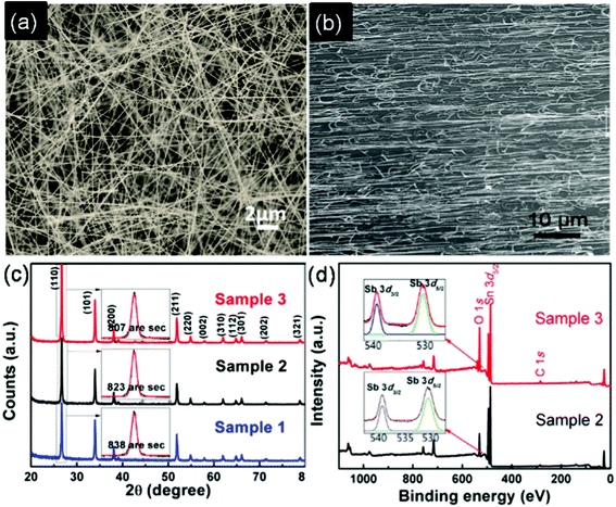 |
| | Fig. 1 Morphology and structural characterization. (a) SEM image of a representative as-grown sample. (b) SEM image of a representative nanonets sample. (c) XRD patterns of three samples, insets show the large magnitude of (110) peaks. (d) XPS spectra of samples 2 and 3, insets show the large magnitude of Sb 3d peaks. | |
3.2. Contact approach for electrical property: field-effect transistor
The traditional contact approach for electrical property characterization is achievable by examining the field-effect transistor (FET) fabricated from the measured materials. The nanonets FET fabrication was obtained through deposition of aluminum source–drain electrodes by thermal evaporation associated with a shadow mask with channel width about 100 μm. Fig. 2(a) shows the typical IDS–VGS curves obtained from these samples and the inset illustrates the configuration of field-effect transistors made from nanonets. Fig. 2(b)–(d) display the typical output characteristics IDS–VDS curves of samples 1, 2, and 3, respectively. Evidently, all the nanonets show semiconductor behavior. The gating effect is exhibited and the positive gate voltage leads to the strong increment of source–drain current, indicating all the nanonets are n-type semiconductors. Clearly the magnitude of IDS increases with an increase in Sb doping. However, the gate voltage effect becomes less dominant with the increase in dopant concentration, as revealed by the increasing off current (Fig. 2(a)) or the lesser increment in output current with increasing VGS (Fig. 2(b)–(d)). The reduction of the gate effect is attributed to the large increase of free electron carrier density caused by antimony doping. The electron mobility (μm) in the variable resistance region and carrier concentration (N0) can be calculated using the following equations | |  | (1) |
| |  | (2) |
 |
| | Fig. 2 Contact method characterizations. (a) Typical output IDS–VGS characteristic curves. Inset shows the diagram of the nanonets FET configuration. Typical output IDS–VDS characteristic curves of (b) sample 1, (c) sample 2, and (d) sample 3. | |
where L and W are the channel length and channel width of the device, respectively. Ci is gate capacitance, and for nanonets device calculation, a standard parallel plate model is employed to estimate the gate capacitance.4Vth is the threshold voltage and d is the thickness of the nanonets. Here, the thickness approximates to the diameter of the nanowires. The calculated electron mobility for samples 1, 2, and 3 are 11.5, 6.6 and 4.8 cm2 V−1 s−1 while the carrier density is estimated to be 0.6 × 10¹⁸, 17.8 × 10¹⁸ and 53.4 × 1018 cm−3, respectively. The dc conductivity of the nanonets could be estimated from the IDS–VDS characteristic curves (Vg = 0) and the corresponding values of different samples are calculated to be ca. 567, 1911 and 2612 Ω−1 m−1. All the values of electron mobility, carrier density and conductivity of these nanonets calculated through this contact method are listed in Table 1 for further comparison with those obtained from the non-contact method.
Table 1 The carrier density, electron mobility and dc conductivity of three samples obtained by contact FET measurement and non-contact THz-TDS measurement
| Sample |
N
0 (×1018 cm−3) |
μ
m (cm2 V−1 s−1) |
σ
0 (Ω−1 m−1) |
| FET |
TDS |
FET |
TDS |
FET |
TDS |
| 1 |
0.6 |
4.05 |
11.5 |
77.62 |
567 |
1350 |
| 2 |
17.8 |
42.4 |
6.6 |
34.56 |
1911 |
2949 |
| 3 |
53.4 |
85.3 |
4.8 |
32.29 |
2612 |
3976 |
The transmitted THz pulsed waves through the reference (blank substrate) and a representative sample were recorded in time-domain by altering the delay time between the THz pulse and gating optical pulse. Fig. 3(a) displays the time-domain spectra of the reference and a representative sample. Compared to the reference signal, the main transmitted pulse peak intensity of the sample shows a significant decrease due to absorption. In each time-domain spectrum of Fig. 3(a), the first transient is the pristine pulse propagated directly through the media. The second transient is attributed to multiple reflections inside the media. Due to the clean separation in time between the main transmitted pulse and the first internal reflected pulse, the data analysis was performed on the main transmitted pulse only without loss of validity. Fig. 3(b) presents the corresponding amplitude spectra in frequency domain after applying fast Fourier transform on the time-domain spectra in Fig. 3(a).
 |
| | Fig. 3 Measured time-domain THz pulses transmitted through a reference and a representative sample. (b) Amplitude spectra in frequency-domain from Fourier transform of (a). | |
THz pulse passing through material is modified by the reflection and transmission at surface and interface, absorption of the material and dispersion in the material. From the complex amplitude ratio of the transmitted THz pulses from the sample Ẽsam(ω) and reference Ẽref(ω), the complex transmission coefficient, ![[t with combining tilde]](https://www.rsc.org/images/entities/i_char_0074_0303.gif) (ω), is given as
(ω), is given as
| |  | (3) |
Where ñ and d are the complex refractive index and thickness of nanonets, respectively. ñs is the refractive index of substrate.
The complex refractive index ñ(ω) can be extracted from eqn (3) by numerical iteration, which enables derivation of other parameters characterizing the electrical and optical properties of the nanonets, by the following relationships:
| |  | (4) |
Where ![[small epsilon, Greek, tilde]](https://www.rsc.org/images/entities/i_char_e0de.gif) (ω) is the frequency dependent complex dielectric response and
(ω) is the frequency dependent complex dielectric response and ![[small sigma, Greek, tilde]](https://www.rsc.org/images/entities/i_char_e10d.gif) (ω) is the complex conductivity of the sample, respectively. ε0 is the free space permittivity and ε∞ is the high frequency dielectric constant, ε∞ = 3.8 for SnO2. Hence combining eqn (3) and (4), the refractive index (black circle in Fig. 4), extinction coefficient κ(ω) (red circle in Fig. 4) which is related to power absorption coefficient (α(ω)) as, κ(ω) = α(ω)c/2ω, complex conductivity of the three samples can be obtained and presented in Fig. 4 and 5, respectively. It should be noted that, since the nanonets comprise of loosely lying nanowires and nitrogen, the physical properties directly measured from the spectra of THz time-domain waveforms include the contributions of both nitrogen and pure nanowires. To obtain the physical parameters of the pure nanowires, a brief effective medium approximation,17,18(ω) = fs(ω) + (1 − f)h(ω)is used, here s(ω) and h(ω) are the complex permittivity of pure nanowires and the host medium (N2), respectively. The filling factor f ∼ 0.07 is obtained from the SEM image shown in Fig. 1(b).
(ω) is the complex conductivity of the sample, respectively. ε0 is the free space permittivity and ε∞ is the high frequency dielectric constant, ε∞ = 3.8 for SnO2. Hence combining eqn (3) and (4), the refractive index (black circle in Fig. 4), extinction coefficient κ(ω) (red circle in Fig. 4) which is related to power absorption coefficient (α(ω)) as, κ(ω) = α(ω)c/2ω, complex conductivity of the three samples can be obtained and presented in Fig. 4 and 5, respectively. It should be noted that, since the nanonets comprise of loosely lying nanowires and nitrogen, the physical properties directly measured from the spectra of THz time-domain waveforms include the contributions of both nitrogen and pure nanowires. To obtain the physical parameters of the pure nanowires, a brief effective medium approximation,17,18(ω) = fs(ω) + (1 − f)h(ω)is used, here s(ω) and h(ω) are the complex permittivity of pure nanowires and the host medium (N2), respectively. The filling factor f ∼ 0.07 is obtained from the SEM image shown in Fig. 1(b).
 |
| | Fig. 4 Measured refractive index (open black circles) and extinction coefficient (open red circles) of (a) sample 1, (b) sample 2, and (c) sample 3. The theoretical fittings are obtained by the Drude–Smith model. | |
 |
| | Fig. 5 Measured real component (solid black circles) and imaginary component (solid red circles) of complex conductivity of (a) sample 1, (b) sample 2, and (c) sample 3. The theoretical fittings are obtained by the Drude–Smith model. | |
The far-infrared dielectric response of doped semiconductors are mainly ascribed to free carriers in the frequency range below transverse optical phonon frequency, where the contribution of the polar crystal lattice mode to the dielectric response is negligible. As shown in Fig. 4, the refractive indices of three nanonets decrease with increasing frequency. Similar phenomena were observed in single crystalline n-type ZnO epilayer19,20 and InN nanorods.21 The calculated refractive index increases with increasing Sb concentration, due to the higher free carrier density with increasing dopant concentration. The far-infrared absorption of semiconductors in the THz region is very sensitive to free carrier concentration. The THz wave propagating in semiconductors causes the movement of carriers and resulting in energy lost by free carriers damping. As shown in Fig. 4, the extinction coefficient of doped samples is higher than that of pure SnO2 nanonets (sample 1), due to higher free carrier concentration in doped samples.
The contribution of free carrier to the optical and electrical properties of semiconductors in the spectral region below the fundamental band gap is determined by the intraband transitions of the partially filled bands. Following the classical dispersion theory, and considering the spatial constraints of free carrier scattering in nanostructures, this intraband transition finally leads to the Drude–Smith theory, for which the complex conductivity is defined by22
| |  | (5) |
where dc conductivity σ0 is given by N0e2τ/m*, N0 is the electron density, e is the electron charge, τ is the relaxation time and m* is the electron effective mass. For SnO2, m* = 0.31 m0,23 where m0 is the mass of free electron. cj is a parameter describing the fraction of the free carrier's original velocity after j numbers of scattering events. Actually, the first term c1 is sufficient in describing the normal physical properties and then c1 varies between −1 and 0, corresponding to a complete backscattering for c1 = −1 and a simple Drude conductivity for c1 = 0. Combining eqn (4) with eqn (5), the frequency dependence of refractive index and extinction coefficient fit well with the Drude–Smith model.
The measured frequency dependence complex conductivity of the three n-type nanonets with different free carrier concentrations were analyzed using the Drude–Smith model, as the solid line shows in Fig. 5. Real parts of the complex conductivity gradually increase with increasing frequency, while imaginary parts displaying negative values that decrease with increasing frequency. The best fitting parameters are shown in Table 2. Evidently, both the real and imaginary aspects of the complex conductivity can be well fitted by the Drude–Smith model, while the samples with higher Sb-dopant concentration present higher conductivity ascribed to higher free carrier concentration. The important parameter, c1, indicates large negative values for all of the three samples and fitted as −0.74, −0.85, and −0.91 for sample 1, 2, and 3, respectively. The increasing c1 value with dopant concentration indicates that the localized electrons might experience a preferential backward scattering from defects in nanowires caused by increased structural disorders24 due to Sb-doping or a Coulombic restoring force ascribed to charged defects.19 To illustrate this content more quantitatively, the electron mean free path of the three samples at room temperature (T ∼300 K) were calculated. With an estimated thermal velocity of  ms−1, the measured scattering time of 13.7, 6.1 and 5.7 fs for sample 1, 2 and 3 result in the mean free path of 1.64, 0.73 and 0.68 nm, which are much smaller than the average nanowire radius of ca. 60 nm. Therefore, we expect that free carriers would undergo simple Drude-like scattering (c = 0) as well as backscattering (c = 1) within the nanowires. However, with the dopant concentration increasing, the mean free path of the free carriers decreases dramatically due to the increased structural defects and spatial constraints. The effective electrical parameters of these three samples, free carriers concentration, N0, obtained from the best fitting THz-TDS data, electron mobility, μm = (1 + c)(eτ/m*) , dc conductivity, σ0 = N0e2τ/m*, were calculated and listed in Table 1. Evidently, the carrier density obtained from the contact method is lower than that from the non-contact method. This is probably due to the nanowire–nanowire junctions which could behave like energy barrier and localized states in the networks during the contact measurement. Mobility is a phenomenological parameter inferring the carrier scattering rate. It reveals the property of electrons population rather than an individual electron.25 In the case of THz-TDS measurements, the electron states could be populated by free carriers substantially at equilibrium in a weak field. The carrier mobility is related to the statistical condition of the carrier momentum relaxation time τ at equilibrium.26 In the FET measurement, the studied carriers are being affected and perturbed by a larger electrical field. They distributed to higher energy states than those at equilibrium or quasi-equilibrium. Their mobility would be determined by the scattering processes and energy relaxation at higher energies where the relaxation time τ is small.27 As listed in Table 1, the field-effect mobility is almost a fraction of the TDS mobility for each sample. Similar results were also shown by Kozawa et al. in their Raman spectra and Hall measurements28 as well as by Li et al. in their IR spectra study of GaN thin film.27 However, both the FET and TDS revealed a clear trend of decreasing mobility with the increases in dopant concentration. This behavior is typically attributed to the coulomb scattering of charged impurity as well as the free carrier interactions.29 Compared with the values obtained through the contact measurement method, the dc conductivity of these three samples exhibits higher values by calculation from the THz-TDS spectra. This is possibly attributed to the contact resistance between the Al electrodes and the nanonets30 as well as the extra energy barrier formed at the nanowire–nanowire junctions.15 As indicated, the Sb-doping would not only reduce the depletion layer of the nanowires but also tend to reduce the junction barrier. Therefore, with the increase in dopant concentration, less distinction of the conductivity values are presented between the contact method and non-contact method as shown in Table 1.
Table 2 Best fitting parameters using the Drude–Smith model
| Sample |
ω
p
/2π (THz) |
τ (fs) |
c
|
| 1 |
32.9 |
13.7 |
−0.74 |
| 2 |
106.6 |
6.1 |
−0.85 |
| 3 |
151.2 |
5.7 |
−0.91 |
4. Conclusions
In summary, we have investigated the electrical parameters of three SnO2 nanonets with different Sb dopant concentrations through a contact approach (FET) and a non-contact approach (THz-TDS). These nanonet FET devices exhibit good device characteristics and the doping effects are well revealed by the device performance. Simultaneously, the same objective is achieved through analyzing the THz-TDS spectra using the Drude–Smith model. To some extent, the THz-TDS spectra reveal more intrinsic physical parameters of the materials due to the absence of extra influences such as contact resistance introduced by electrodes deposition and junction barriers formed by electron transport from nanowire to nanowire.
References
- A. J. Baca, J.-H. Ahn, Y. Sun, M. A. Meitl, E. Menard, H.-S. Kim, W. M. Choi, D.-H. Kim, Y. Huang and J. A. Rogers, Angew. Chem., Int. Ed., 2008, 47, 5524 CrossRef CAS.
- Y.-J. Choi, I.-S. Hwang, J.-G. Park, K. J. Choi, J.-H. Park and J.-H. Lee, Nanotechnology, 2008, 19, 095508 CrossRef.
- B. Wang, L. F. Zhu, Y. H. Yang, N. S. Xu and G. W. Yang, J. Phys. Chem. C, 2008, 112, 6643 CAS.
- E. N. Dattoli, Q. Wan, W. Guo, Y. Chen, X. Pan and W. Lu, Nano Lett., 2007, 7, 2463 CrossRef CAS.
- Z. Liu, D. Zhang, S. Han, C. Li, T. Tang, W. Jin, X. Liu, B. Lei and C. Zhou, Adv. Mater., 2003, 15, 1754 CrossRef CAS.
- S. Gubbala, V. Chakrapani, V. Kumar and M. K. Sunkara, Adv. Funct. Mater., 2008, 18, 2411 CrossRef CAS.
- P. Nguyen, H. T. Ng, J. Kong, A. M. Cassell, R. Quinn, J. Li, J. Han, M. McNeil and M. Meyyappan, Nano Lett., 2003, 3, 925 CrossRef CAS.
- Q. Wan, E. Dattoli and W. Lu, Small, 2008, 4, 451 CrossRef CAS.
- Q. Wan, E. N. Dattoli and W. Lu, Appl. Phys. Lett., 2007, 90, 222107 CrossRef.
- J. T. Darrow, B. B. Hu, X. C. Zhang and D. H. Auston, Opt. Lett., 1990, 15, 323 CrossRef CAS.
- X. Xie, J. Dai and X. C. Zhang, Phys. Rev. Lett., 2006, 96, 075005 CrossRef.
- J. Dai, X. Xie and X. C. Zhang, Phys. Rev. Lett., 2006, 97, 103903 CrossRef.
- K. Takahashi, N. Kida and M. Tonouchi, Phys. Rev. Lett., 2006, 96, 117402 CrossRef.
- M. Tonouchi, Nat. Photonics, 2007, 1, 97 CrossRef CAS.
- C. Sun, N. Mathews, M. Zheng, C. H. Sow, L. H. Wong and S. G. Mhaisalkar, J. Phys. Chem. C, 2009, 114, 1331 Search PubMed.
- Z. Fan, J. C. Ho, Z. A. Jacobson, R. Yerushalmi, R. L. Alley, H. Razavi and A. Javey, Nano Lett., 2007, 8, 20 CrossRef.
- F. J. García-Vidal, J. M. Pitarke and J. B. Pendry, Phys. Rev. Lett., 1997, 78, 4289 CrossRef.
- H. C. Weissker, J. Furthmüller and F. Bechstedt, Phys. Rev. B: Condens. Matter, 2003, 67, 165322 CrossRef.
- J. B. Baxter and C. A. Schmuttenmaer, J. Phys. Chem. B, 2006, 110, 25229 CrossRef CAS.
- X. H. Zhang, H. C. Guo, A. M. Yong, J. D. Ye, S. T. Tan and X. W. Sun, J. Appl. Phys., 2010, 107, 033101 CrossRef.
- H. Ahn, Y. P. Ku, Y. C. Wang, C. H. Chuang, S. Gwo and C.-L. Pan, Appl. Phys. Lett., 2007, 91, 163105 CrossRef.
- N. V. Smith, Phys. Rev. B: Condens. Matter, 2001, 64, 155106 CrossRef.
- H. J. van Daal, Solid
State Commun., 1968, 6, 5 CrossRef CAS.
- C. H. Shen, H. Y. Chen, H. W. Lin, S. Gwo, A. A. Klochikhin and V. Y. Davydov, Appl. Phys. Lett., 2006, 88, 253104 CrossRef.
-
B. K. Ridley, Quantum Processes in Semiconductors, Clarendon, Oxford, 1982 Search PubMed.
- R. Ulbricht, E. Hendry, J. Shan, T. F. Heinz and M. Bonn, Rev. Mod. Phys., 2011, 83, 543 CrossRef CAS.
- Z. F. Li, W. Lu, H. J. Ye, Z. H. Chen, X. Z. Yuan, H. F. Dou, S. C. Shen, G. Li and S. J. Chua, J. Appl. Phys., 1999, 86, 2691 CrossRef CAS.
- T. Kozawa, T. Kachi, H. Kano, Y. Taga, M. Hashimoto, N. Koide and K. Manabe, J. Appl. Phys., 1994, 75, 1098 CrossRef CAS.
-
S. M. Szein Physics of Semiconductor Devices, Wiley, New York, 2nd edn, 1981, pp. 29 Search PubMed.
- M. S. Arnold, P. Avouris, Z. W. Pan and Z. L. Wang, J. Phys. Chem. B, 2002, 107, 659 CrossRef.
Footnote |
| † These authors made an equal contribution to this work. |
|
| This journal is © The Royal Society of Chemistry 2012 |
Click here to see how this site uses Cookies. View our privacy policy here.