Enhanced light harvesting in bulk heterojunction photovoltaic devices with shape-controlled Ag nanomaterials: Ag nanoparticles versus Ag nanoplates†
Dong Hwan
Wang
ab,
Jung Kyu
Kim
b,
Guh-Hwan
Lim
e,
Keum Hwan
Park
c,
O Ok
Park
cd,
Byungkwon
Lim
*e and
Jong Hyeok
Park
*b
aCenter for Polymers and Organic Solids, University of California at Santa Barbara, Santa Barbara, CA 93106-5090, USA
bSchool of Chemical Engineering and SAINT, Sungkyunkwan University, Suwon, 440-746, Republic of Korea. E-mail: lutts@skku.edu
cDepartment of Chemical and Biomolecular Engineering, Korea Advanced Institute of Science and Technology (BK 21 Graduate Program), 373-1 Guseong-dong, Yuseong-gu, Daejeon, 305-701, Republic of Korea
dDepartment of Energy Systems Engineering, Daegu Gyeongbuk Institute of Science and Technology (DGIST), 50-1, Sang-ri, Hyeonpung-myeon, Dalseong-gun, Daegu, 711-873, Republic of Korea
eSchool of Advanced Materials Science and Engineering, Sungkyunkwan University, Suwon, 440-746, Republic of Korea. E-mail: blim@skku.edu
First published on 12th July 2012
Abstract
Enhanced power conversion efficiency (PCE(%)) with improved optical path length from two types of shape controlled silver (Ag) materials (Ag nanoplates versus Ag nanoparticles (NPs)) was studied in poly(3-hexylthiophene) (P3HT)/[6,6]-phenyl C71 butyric acid methyl-ester (PC71BM) or poly[N-9′′-hepta-decanyl-2,7-carbazole-alt-5,5-(4′,7′-di-2-thienyl-2′,1′,3′-benzothiadiazole)] (PCDTBT)/[6,6]-phenyl C71 butyric acid methyl-ester (PC71BM) bulk heterojunction (BHJ) devices. The Ag nanoplates and Ag NPs can be synthesized by simple solution polyol chemistry with well defined size and shape. A BHJ with a 0.5 wt% optimized blend ratio of Ag nanoplates shows improved cell performance and photo-current density than a BHJ with Ag NPs owing to the enhanced light absorption with the results of an excitation of localized surface plasmon and efficient light scattering by the Ag nanoplates embedded BHJ film. When the BHJ is combined with the Ag nanoplates at an optimized ratio of 0.5 wt%, the PCE (%) increases from 3.2% to 4.4% in P3HT/PC71BM, and from 5.9% to 6.6% in PCDTBT/PC71BM BHJ devices.
Introduction
Bulk heterojunction (BHJ) photovoltaic devices based on polymer–fullerene have been widely researched on account of their numerous advantages. Specifically, they can be fabricated in a large area with a simple method; they are flexible low-cost devices that involve a roll-to-roll manufacturing process; and their industrial application has great potential for the future.1–8 The efficiency of photovoltaic devices has gradually increased from 2% to 8% as a result of various meaningful studies. The studies have focused on diverse aspects, such as solvent additives,9 thermal treatment,10,11 newly designed donor–acceptor polymers,12 donor–acceptor blend ratios,13,14 efficient nanopatterned structural effects (tandem or regular patterns),15–17 the plasmonic embedded nanoparticles (NPs) effect,18–21 and other novel processes (involving transfers and printing).22,23Silver (Ag) metal NPs exhibit a localized surface plasmon resonance (LSPR) that is coupled tightly with the incident light. Moreover, metallic NPs larger than 10 nm can scatter and reflect the incident light, thereby increasing the length of the optical path within the BHJ active layer film. Especially, the shape and size of Ag materials can be easily controlled, have efficient reproducibility and higher yields than other metallic NPs. Thus, the embedding of metal NPs in BHJ film offers the possibility of enhanced optical absorption. The power conversion efficiency (PCE (%)) leads to a corresponding enhancement of the photo-generation of mobile carriers. Hence, when Ag is embedded in BHJ films, the different shapes of the Ag particles produce dissimilar absorption properties and different levels of reflectivity.20,21
In a BHJ solar cell, the active layer (which has the maximum efficiency) generally has a thickness of less than 200 nm. One of the major roles of Ag nanomaterials in a BHJ solar cells is its effective light scattering effect. To maximize the effectiveness of Ag nanomaterials, researchers generally prefer to use large rather than small materials. Unfortunately, the restricted thickness of BHJ film makes it impossible to use Ag nanomaterial that is larger than 200 nm. However, a 2 dimensional nanostructure with a high aspect ratio can overcome this constraint if the material can be spread horizontally on a target substrate during the spin-coating process.21 This assumption is reasonable because the intensification of the van der Waals interactions between the Ag nanoplate surface and the target surface stem primarily from the structural characteristics of the 2D nanosheets.24 Therefore, when the Ag nanoplates are sheared during the spin-coating of the poly(3,4-ethlyene dioxythiophene)![[thin space (1/6-em)]](https://www.rsc.org/images/entities/char_2009.gif) :poly(styrene sulphonate) (PEDOT:PSS) surface, they tend to be oriented horizontally on the PEDOT:PSS surface.
:poly(styrene sulphonate) (PEDOT:PSS) surface, they tend to be oriented horizontally on the PEDOT:PSS surface.
This research compares two different shape-controlled Ag materials (Ag NPs and Ag nanoplates) embedded in BHJ photovoltaic cells fabricated with either poly(3-hexylthiophene) (P3HT)/[6,6]-phenyl C71 butyric acid methyl-ester (PC71BM) or poly[N-9′′-hepta-decanyl-2,7-carbazole-alt-5,5-(4′,7′-di-2-thienyl-2′,1′,3′-benzothiadiazole)] (PCDTBT)/[6,6]-phenyl C71 butyric acid methyl-ester (PC71BM). When they are embedded in the BHJ, the Ag NPs and Ag nanoplates have different absorption spectra and optical reflectance levels, and these differences strongly affect the cell. To compare and investigate how the shape of Ag materials affects the performance of photovoltaic devices, we blended the Ag NPs and Ag nanoplates into a BHJ solution with various weight ratios ranging from 0.1 wt% to 1 wt%. Ag nanoplates are also well dispersed in the BHJ film after the spin-coating process. At an optimized blend ratio of 0.5 wt% with Ag nanoplates in BHJ film, the PCE increased from 3.2% to 4.4% for the P3HT/PC71BM and from 5.9% to 6.6% for the PCDTBT/PC71BM, owing to the light-trapping effect and the enhanced optical path length in the active layer.
Experimental
Synthesis of Ag NPs
We used AgNO3 (Aldrich) as the precursor of the Ag NPs and poly(vinylpyrrolidone) (PVP) (Aldrich, Mw = 55000) as the surfactant. In a typical synthesis, we mixed 3.0 mL of a 94 mM sample of AgNO3, 3.0 mL of a 147 mM sample of PVP, and 6 mL of polyol. We then heated the mixture at 140 °C for 1 h. To control the 30 nm-sized Ag NPs, we used an optimized 1,5-pentanediol (PtD: Aldrich) solvent. The smaller NPs were synthesized in a more viscous medium. For example, the polyol viscosity increases as the hydrocarbon chain is elongated in the order of PtD > 1,4-butanediol (BD: Sigma Aldrich) > PrD 1,2-propanediol (PrD: Sigma Aldrich). The size of the synthesized NPs then decreases in the order of PrD (60 nm) > BD (40 nm) > PtD (30 nm). Lastly, we added ethanol for the centrifugation process and then collected the synthesized Ag NPs in vials.
Synthesis of Ag nanoplates
Ag nanoplates were synthesized via an aqueous-phase route, as reported elsewhere.25 In a typical synthesis, we heated 8 mL of an aqueous solution containing PVP (Mw = 29000, 100 mg, Aldrich) at 60 °C in air under magnetic stirring. In addition, AgNO3 (95.8 mg, Aldrich) was dissolved in 3 mL of deionized water at room temperature. The aqueous solution of AgNO3 was added to the PVP solution, and the reaction mixture was then aged at 60 °C in air for 21 h. After the synthesis, the product was collected by centrifugation, washed with ethanol to remove the excess PVP, and then re-dispersed in water.
Device fabrication
P3HT, PCBM and PCDTBT was purchased from Rieke Metal, Nano-C and 1-Material, respectively. Polymer solar cells based on P3HT/PC61BM, P3HT/PC71BM or PCDTBT/PC71BM with a blend of Ag materials from NPs or nanoplates were prepared as shown in Fig. 1. Because of surface impurities, the ITO glass substrate was step by step cleaned with solvents of chloroform, acetone, and isopropanol, respectively with an ultra-sonic process. The ITO glass was then exposed to UV for 15 min to reform the surface before the spin-casting of PEDOT:PSS (Baytron PH) for 5000 rpm at 40 s. After the spin-casting of PEDOT:PSS, the substrate was baked at 140 °C for 10 min to evaporate the solvent. On top of the PEDOT/PSS layer, we made a 120 nm (P3HT/PCBM for 2000 rpm at 20 s) or an 100 nm (PCDTBT/PC71BM for 5000 rpm at 40 s) BHJ active layer with Ag NPs or nanoplates with a weight ratio of 0.1 wt%, 0.5 wt%, and 1 wt% in a mixed solution of P3HT/PCBM (1:0.8) in a chlorobenzene solvent or PCDTBT/PC71BM (1:4) in 1,2-dichlorobenzene:chlorobenzene (3:1), respectively. The reference device was composed of a plain donor–acceptor BHJ without any Ag materials. The BHJ films were dried at 80 °C for 10 min in a glove box. The TiOx interlayer was then spin-coated in air at room temperature to a thickness of 10 nm (5000 rpm, 40 s). An Al metal cathode was thermally deposited by means of an evaporator to a thickness of 100 nm at a pressure of 5.0 × 10⁻⁶ Torr. The device efficiency levels were measured with a solar simulator (Air Mass 1.5 Global) at an intensity of 1000 Wm−2. A Keithley 236 source measure unit was also used to characterize the voltage–current density of each device. All the cell areas were accurately measured by the SV-35 video microscope system (SOMETECH). The surface morphology of the BHJ film was analyzed with the aid of a scanning electron microscope (SEM, FEI Sirion XL 30) and an atomic force microscope (Veeco, USA; D3100).
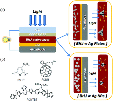 | ||
| Fig. 1 (a) A schematic diagram of the devices with two different Ag materials (Ag nanoplates and Ag NPs); (b) the chemical structures of P3HT and PCDTBT of the donor and PC71BM of the acceptor. | ||
Results and discussion
Fig. 1(a) shows the schematic diagram of the devices with two different shapes of Ag materials of NPs or nanoplates. Fig. 1(b) reveals the chemical structures of the donor polymers P3HT and PCDTBT, and acceptor polymer PC71BM.The shape of the synthesized Ag materials was confirmed with SEM images. As shown in Fig. 2(a) and Fig. 2(b), the NP diameter is ∼40 nm and the nanoplate diameter is ∼200 nm to 500 nm. The UV-visible absorption spectra of Fig. 2(c) show that the synthesized Ag NPs have an maximum absorption peak near 420 nm; they also show that the nanoplates have a very broad peak of 400 nm to 800 nm. The analysis results from energy dispersive spectroscopy in Fig. S1 (ESI†) show that the synthesized nanoplates were composed of an Ag element. Furthermore, the different shapes of the Ag materials have a different colour when Ag is dispersed in ethanol. The Ag NPs are dark green and the Ag nanoplates are light gray. For these reasons, the dissimilar shape of the synthesized Ag materials produces different absorption behaviour and the reflective phenomena appear to depend on the shape and size of Ag. Note that the Ag nanoplates can efficiently reflect the incident solar light because the particles are large and the aspect ratio is greater than 50.
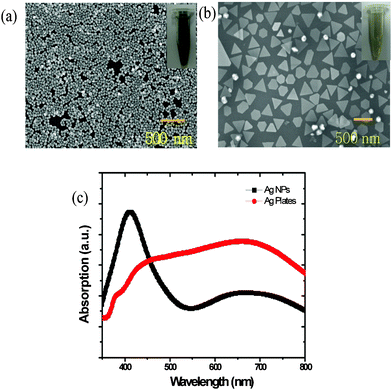 | ||
| Fig. 2 (a) SEM images of the Ag NPs, and (b) Ag nanoplates. The inset figures show the Ag materials dispersed in an ethanol solvent (Ag NPs: dark green; Ag nanoplates: light gray). (c) UV–visible absorption spectra of Ag nanoparticles and Ag nanoplates. | ||
Fig. 3(a) shows the photocurrent–voltage (J–V) curves of plain BHJ (P3HT/PC71BM) devices and BHJ devices embedded with Ag NPs or Ag nanoplates with a 0.5 wt% ratio versus the total weight of the donor–acceptor polymer mixtures.
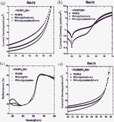 | ||
| Fig. 3 (a) The J–V curves of devices with the plain P3HT/PC71BM BHJ, the BHJ with Ag NPs, and the BHJ with Ag nanoplates from a ratio of 0.5 wt%. (b) The J–V curves of devices with the plain P3HT/PC71BM BHJ, and the BHJ with Ag NPs (0.5 wt%) and nanoplates (0.5 wt%) in the dark current. (c) Diffuse reflectance spectra of the plain P3HT/PC71BM BHJ, the BHJ with Ag NPs (0.5 wt%), and the BHJ with Ag nanoplates (0.5 wt%) as a function of wavelength (nm). (d) J–V curves of devices with the plain PCDTBT/PC71BM BHJ, the BHJ with Ag NPs, and the BHJ with Ag nanoplates for a ratio of 0.5 wt%. | ||
The P3HT/PC71BM BHJ device without Ag materials has a PCE of 3.2%, an open-circuit voltage (Voc) of 0.60 V, a short-circuit current (Jsc) of 11.93 mA cm−2, and a fill factor (FF) of 0.44. In contrast, the BHJ devices with an optimized ratio of 0.5 wt% of Ag NPs or Ag nanoplates have an improved PCE level of 4.0% and 4.4%, respectively. The fact that the photo-current density (Jsc) increased from 11.93 mA cm−2 (for the plain BHJ) to 13.85 mA cm−2 (for the Ag nanoplates) is a key factor in the enhancement of the device performance. The series resistance of the plain BHJ (without Ag) was 8.95 Ωcm2, whereas that of the BHJ with Ag nanoplates was at a lower level of 2.94 Ω cm2. This reduction, as shown in Fig. 3(b), appears to be associated with the higher short circuit currents. The overall device efficiency and average values are summarized in Table 1 and Fig. 4, respectively.
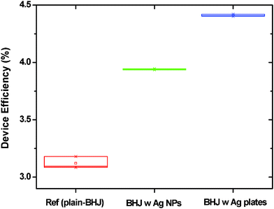 | ||
| Fig. 4 The average P3HT/PC71BM device efficiencies of plain BHJ (reference device), BHJ with Ag NPs, and BHJ with Ag nanoplates. The BHJ device with Ag nanoplates (4.41%, 0.61 V, 13.96 mA cm−2, 0.51) showed increased average power conversion efficiency, open circuit voltage (V), photo-current density (mA cm−2), and FF than the device of plain-BHJ (3.12%, 0.60 V, 12.33 mA cm−2, 0.42) and the BHJ with Ag NPs (3.94%, 0.61 V, 13.11 mA cm−2, 0.49). | ||
| BHJ devices with or without Ag | V oc (V) | J sc (mA cm−2) | FF | Efficiency (%) | |
|---|---|---|---|---|---|
| P3HT/PC71BM | BHJ (ref.) | 0.60 | 11.93 | 0.44 | 3.2 |
| BHJ w/ Ag NPs (0.5 wt%) | 0.62 | 12.95 | 0.50 | 4.0 | |
| BHJ w/ Ag nanoplates (0.5 wt%) | 0.61 | 13.85 | 0.52 | 4.4 | |
| PCDTBT/PC71BM | BHJ (ref.) | 0.90 | 11.63 | 0.57 | 5.9 |
| BHJ w/ Ag NPs (0.5 wt%) | 0.87 | 12.12 | 0.61 | 6.4 | |
| BHJ w/ Ag nanoplates (0.5 wt%) | 0.87 | 13.19 | 0.57 | 6.6 | |
Note also that the ratio of the BHJ active layer and the Ag materials was optimized by varying the concentration from 0.1 wt% to 1 wt%. We used an optimized 0.5 wt% ratio between the active materials and the Ag materials. As shown in Fig. S2 (ESI†) and each inset table, the blending of the P3HT/PC61BM BHJ active layer with Ag NPs or nanoplates at a ratio of more than 0.5 wt% yields a FF value that is less than the FF value of the optimized device.
Fig. 5 shows SEM images of the three kinds of BHJ active layers. Fig. 5(a) shows the plain P3HT/PC71BM BHJ with a clear surface morphology. Fig. 5(b) and 5(c) show the BHJ with 40 nm Ag NPs (0.5 wt%) and the BHJ with Ag nanoplates (0.5 wt%), respectively. These images confirm that the Ag NPs and Ag nanoplates can be well dispersed yet retain their particular shape and size within the BHJ film. Fig. 5(d) shows that the Ag nanoplates were slightly tilted and twisted when blended with the BHJ solution and after the spin-coating process. Interestingly, the surface roughness of the blended film was unchanged when the BHJ was combined with Ag nanoplates. The atomic force microscopy (AFM) results in Fig. S3 (ESI†) confirm that the surface roughness of root mean square (rms) of the plain BHJ (6.9 nm) is similar to that of the Ag nanoplates (5.9 nm).
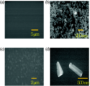 | ||
| Fig. 5 SEM images of the active layer of (a) the plain P3HT/PC71BM BHJ and (b) the BHJ with Ag NPs (0.5 wt%); (c) low-resolution SEM image and (d) high-resolution SEM image of the BHJ with Ag nanoplates (0.5 wt%). | ||
A BHJ film with Ag nanoplates may have superior absorption than the plain BHJ and BHJ with Ag NPs because it can scatter the incident light more effectively on account of the large particle size.4,20 As indicated in the UV-visible absorption spectra (Fig. S4, ESI†), the shape of the Ag nanoplates causes the BHJ film with Ag nanoplates to show more enhanced light absorption than the pure BHJ film or the BHJ film embedded with Ag NPs. The diffuse reflectance spectra of incident light as a function of wavelengths resemble the absorption spectra in Fig. 3(c). This resemblance suggests that the length of the optical path within the BHJ film can be enhanced. Hence, the P3HT/PC71BM BHJ device with Ag nanoplates (0.5 wt%) has a higher level of optical absorbance than the plain P3HT/PC71BM BHJ or the BHJ with Ag NPs at reflectance wavelength of around 400 nm to 500 nm. The scattering effect of the Ag nanoplates increases the effective length of the optical path, which in turn increases the generation of electron–hole pairs.20 The enhanced optical absorbance is closely related to the improved Jsc and PCE levels in the BHJ devices.
The ratio of Ag nanoplates was also optimized in another PCDTBT/PC71BM BHJ active layer to prove the positive effects of Ag nanoplates in universal BHJ devices. The value of FF remained 0.57, and the value of Jsc increased to a critical extent, from 11.63 mA cm−2 to 13.19 mA cm−2 as shown in Fig. 3(d). The BHJ device with Ag nanoplates showed increased average power conversion efficiency (more than ten samples were tested as shown in Fig. S5, ESI†) over the BHJ devices with Ag NPs and without Ag materials. Additionally, all cases of thick and thin active layer BHJ solar cells with Ag nanoplates revealed improved fill factor, PCE (%), and incident photon to current efficiency (IPCE) over the plain BHJ device as shown in Fig. S6 and Fig. S7 (ESI†).
Conclusions
In conclusion, we have demonstrated the positive effects of Ag nanoplates in P3HT/PC71BM and PCDTBT/PC71BM BHJ photovoltaic devices. The BHJ embedded with Ag nanoplates has greater Jsc and PCE values than the plain BHJ and the BHJ with Ag NPs. These results are attributed to the fact that the active layer has an enhanced level of light absorption because the length of the optical path is increased by the efficient scattering and light trapping in the BHJ active films. We believe that the shape of a metal NP is a critical factor in maximizing the light scattering in BHJ solar cells. Finally, a BHJ active layer embedded with Ag nanoplates at a ratio of 0.5 wt% increases the PCE from 3.2% to 4.4% in a P3HT/PC71BM BHJ device and from 5.9% to 6.6% in a PCDTBT/PC71BM BHJ device.Acknowledgements
This work was supported by a grant from the National Research Foundation (NRF) funded by the Korea Ministry of Education, Science and Technology (MEST) (20110023215, 20110027677). J. H. Park acknowledges Future-based Technology Development Program (Nano Fields) through the NRF funded by the MEST (2010-0029321). B.L. was supported by a grant (Code No. 2011-0031628) from the Center for Advanced Soft Electronics under the Global Frontier Research Program of the MEST, Korea.References
- G. Yu, J. Gao, J. C. Hummelen, F. Wudl and A. J. Heeger, Science, 1995, 270, 1789 CAS.
- S. H. Park, A. Roy, S. Beaupre', S. Cho, N. Coates, J. S. Moon, D. Moses, M. Leclerc, K. Lee and A. J. Heeger, Nat. Photonics, 2009, 3, 297 CrossRef CAS.
- A. J. Heeger, Angew. Chem., Int. Ed., 2001, 40, 2591 CrossRef CAS.
- D. H. Wang, D. Y. Kim, K. W. Choi, J. H. Seo, S. H. Im, J. H. Park, O. O. Park and A. J. Heeger, Angew. Chem., Int. Ed., 2011, 50, 5519 CrossRef CAS.
- G. Dennler, M. C. Scharber and C. J. Brabec, Adv. Mater., 2009, 21, 1323 CrossRef CAS.
- D. H. Wang, D. G. Choi, O. O. Park and J. H. Park, J. Mater. Chem., 2010, 20, 4910 RSC.
- C. J. Brabec, S. Gowrisanker, J. J. M. Halls, D. Laird, S. Jia and S. P. Williams, Adv. Mater., 2010, 22, 3839 CrossRef CAS.
- D. H. Wang, J. S. Moon, J. Seifter, J. Jo, J. H. Park, O. Park O and A. J. Heeger, Nano Lett., 2011, 11, 3163 CrossRef CAS.
- C. V. Hoven, X.-D. Dang, R. C. Coffin, J. Peet, T.-Q. Nguyen and G. C. Bazan, Adv. Mater., 2010, 22, E63 CrossRef CAS.
- Ma, C. Yang, X. Gong, K. H. Lee and A. J. Heeger, Adv. Funct. Mater., 2005, 15, 1617 CrossRef CAS.
- C. J. Brabec, N. S. Sariciftci and J. C. Hummelen, Adv. Funct. Mater., 2001, 11, 15 CrossRef CAS.
- L. Huo, J. Hou, S. Zhang, H.-Y. Chen and Y. Yang, Angew. Chem., Int. Ed., 2010, 49, 1500 CrossRef CAS.
- D. H. Wang, J. K. Kim, O. O. Park and J. H. Park, Energy Environ. Sci., 2011, 4, 1434 CAS.
- N. D. Treat, M. A. Brady, G. Smith, M. F. Toney, E. J. Kramer, C. J. Hawker and M. L. Chabinyc, Adv. Energy Mater., 2011, 1, 82 CrossRef CAS.
- S. Sista, M.-H. Park, Z. Hong, Y. Wu, J. Hou, W. L. Kwan, G. Li and Y. Yang, Adv. Mater., 2010, 22, 380 CrossRef CAS.
- D. H. Wang, D. G. Choi, K. J. Lee, J. H. Park and O. O. Park, Langmuir, 2010, 26, 9584 CrossRef CAS.
- D. H. Wang, D. G. Choi, K. J. Lee, S. H. Im, O. O. Park and J. H. Park, Org. Electron., 2010, 11, 1376 CrossRef CAS.
- H. A. Atwater and A. Polman, Nat. Mater., 2010, 9, 205 CrossRef CAS.
- K. Kim and D. L. Carroll, Appl. Phys. Lett., 2005, 87, 203113 CrossRef.
- D. H. Wang, K. H. Park, J. H. Seo, J. Seifter, J. H. Jeon, J. H. Park, O. O. Park and A. J. Heeger, Adv. Energy Mater., 2011, 1, 766 CrossRef CAS.
- C.-H. Kim, S.-H. Cha, S. C. Kim, M. Song, J. Lee, W. Shin, S.-J. Moon, J. H. Bahng, N. A. Kotov and S.-H. Jin, ACS Nano, 2011, 5, 3319 CrossRef CAS.
- F. C. Krebs, S. A. Gevorgyan and J. Alstrup, J. Mater. Chem., 2009, 19, 5442 RSC.
- F. C. Krebs, Sol. Energy Mater. Sol. Cells, 2009, 93, 1636 CrossRef CAS.
- J. N. Israelachvili, Intermolecular and surface forces, Academic Press, London 1992 Search PubMed.
- Y. Xiong, I. Washio, J. Chen, H. Cai, Zhi.-Y. Li and Y. Xia, Langmuir, 2006, 22, 8563 CrossRef CAS.
Footnote |
| † Electronic Supplementary Information (ESI) available. See DOI: 10.1039/c2ra20815f/ |
| This journal is © The Royal Society of Chemistry 2012 |