The periodically negative semi-pyramid nanostructured polymer layer for broadband anti-reflection effect†
Jong-Chang
Woo‡
a,
Nam Seob
Baek‡
b,
Joo Yeon
Kim
*c and
Chang-Il
Kim
a
aSchool of Electrical and Electronics Engineering, Chung-Ang University, 221 Heukseok-Dong, Dongjak-Gu, Seoul, 156-759, Korea
bIT Convergence Technology Research Lab., Electronics and Telecommunications Research Institute (ETRI), Daejeon, Korea
cNext Generation Display Research Division, Component and Materials Research Department, Electronics and Telecommunications Research Institute (ETRI), Daejeon, Korea. Fax: 82-42-860-5202; Tel: 82-42-860-6216E-mail: jooyeon.kim@etri.re.kr
First published on 2nd August 2012
Abstract
The periodic negative semi-pyramid nanostructures are fabricated in polymer layer via an imprinting-assisted replication process using the differentially shaped, but periodically textured Si-masters demonstrating the effective reduced reflectance of less than 20% over broadband wavelengths ranging from 300 nm to 1200 nm.
Silicon (Si)-based optical and optoelectronic devices, such as solar cells, flat displays, and light sensors, require the understanding and study of the reflection of incident light at the air–Si interface because of their refractive index differences.1,2 This non-continuous interface causes high reflection of incident light of more than 30%, and this is the main obstacle to improving the light collecting performance of many devices. Therefore, there has been a great deal of effort to reduce the light reflection limits by combining surface coating methods, which is the most common way to suppress the light reflection produced by layer-by-layer film deposition based on SiO2 and TiO2via the sputtering method.3,4 However, to coat the surface with films, it is necessary to find materials to match the refractive index of the under layer, and the materials must be transparent over broadband wavelengths. Moreover, single- or multi-layer film deposition methods require high-temperature processing and may result in process incompatibility and high processing costs. However, these drawbacks can be resolved by surface patterning to produce a graded refractive index to enhance the anti-reflective (AR) efficiency over broadband wavelengths.
Over the past decade, differentially surface-patterned structures, such as nanowires, nanopillars, and nanorod arrays, have been directly introduced on a Si surface to minimize the reflection at interfaces.5–10 However, the fabrication processes to obtain these structures are not simple due to the complex techniques used, such as electron-beam lithography and laser interface lithography.11,12 Moreover, there are serious challenges for low cost large area production.
Therefore, imprinting techniques have been considered as alternative approaches in the fabrication of micro- and nano-scale structures over large areas. This has several advantages including low cost, high throughput, and high resolution for submicron scale structures.13,14 Moreover, it has been demonstrated that the imprinting technique is suitable for the replication of structures in the polydimethylsiloxane (PDMS) layer to generate feature sizes in the submicron domain.15 The as-formed structured PDMS layer ensures good conformal contact with the substrate, even during detachment from the master. These advantages guarantee a good pattern transfer into the PDMS layer.
In this paper, the periodically negative semi-pyramid nanostructured PDMS AR layers with three different geometrical profiles were fabricated via an imprinting-assisted replication process. The imprinting was performed by pressing the PDMS pre-polymer covered with a periodically textured Si-master in direct contact, which is suitable for making a patterned layer on various substrates, such as Si, glass, and planar substrates. The textured periodic structures on the Si-master were transferred into the PDMS layer as negative profiles. The reflectance of the periodically textured Si-masters and replicated negative semi-pyramid nanostructured PDMS AR layers was measured, and their differences were compared with the reflectance of a bare Si-wafer as a reference over broadband wavelengths from 300 nm to 1200 nm.
Fig. 1 shows typical scanning electron microscopy (SEM) images of the periodically textured Si-masters with cross-sectional view (Fig. S1, ESI†). The SEM images reveal that the created periodic textures are tapered positive semi-pyramid profiles with negative semi-parabolic shapes with heights of approximately 500 nm, 650 nm, and 1000 nm.
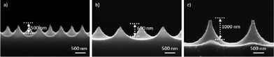 | ||
| Fig. 1 The SEM images of the periodically textured Si-masters with the different depth profiles of (a) 500 nm, (b) 650 nm, and (c) 1000 nm. | ||
To improve the pattern transfer from the periodically textured Si-master into the PDMS layer, the surface of the periodically textured Si-master was chemically treated with trichloro(1H,1H,2H,2H-perfluorooctyl) silane (FOTS). The effectiveness of the surface treatment was confirmed by contact angle measurement using a water drop goniometer. The water contact angle differences in the air between the untreated and FOTS-treated periodically textured Si-masters were measured and are presented in Fig. 2(a). The water contact angles for the untreated periodically textured Si-master with three different profiles with heights of 500 nm, 650 nm, and 1000 nm were measured and ranged from 48° to 82°. Normally, untreated Si-wafers are extremely hydrophilic with a contact angle less than 30°. However, the periodically textured Si-master in this work demonstrated a slightly increased contact angle influenced by the surface contamination such as photoresist or other organic residues originating from manufacturing processes.16 After the FOTS treatment on the periodically textured Si-master, the water contact angles ranged from 108° to 153° and it greatly increased from 48° to 153 ± 0.5° for a texture depth of 500 nm (see insets in Fig. 2(a)). This resulted in lower surface energy and facilitated easy detachment of the Si-master from the imprinted PDMS AR layer without contamination by residue or deformation by adhesion force between the periodically textured Si-master and the PDMS AR layer.
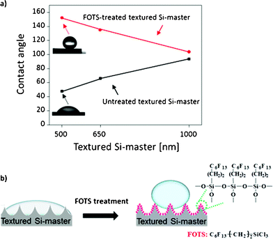 | ||
| Fig. 2 (a) Water contact angles of the untreated and FOTS-treated periodically textured Si-masters with three different heights of 500 nm, 650 nm, and 1000 nm, respectively. (b) A schematic diagram of the water drop on the untreated (left) and FOTS-treated periodically textured Si-master (right) showing a behaviour similar to the hydrophobic nano-grass effect. | ||
The hydrophobic surface with a high contact angle achieved by fabricating the periodically textured surface with differently scaled nanostructures and chemical treatments can be explained by Wenzel's model (eqn (1)) and Cassie's model (eqn (2)) constructed as follows:17,18
| cosθr = rcosθ | (1) |
| cosθr = f1cosθ − f2 | (2) |
Fig. 3 shows SEM images of the imprinted PDMS AR layers. The total size of the negative semi-pyramid nanostructured PDMS AR layer transferred patterns from the FOTS-treated periodically textured Si-master was 2 × 2 cm2. The negative semi-pyramid nanostructures in the PDMS layer after imprinting lithography have approximately the same geometrical profiles of the height as the periodically textured Si-master of 500 nm, 650 nm, and 1000 nm texture depths. The notable geometrical measurements of the negative semi-pyramid nanostructured PDMS AR layer are the depth from the top surfaces of the open areas and the differentially tapered shapes as shown in Fig. 3 (d), (e), and (f).
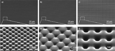 | ||
| Fig. 3 The SEM images of the negative semi-pyramid nanostructured PDMS AR layers. (a) to (c) have the different depth profiles of 500 nm, 650 nm, and 1000 nm, respectively, which were replicated from the periodically textured Si-master as shown in Fig. 1 (a) to (c). (d) to (f) are zoomed-in views of (a) to (c). | ||
To investigate the AR efficiencies, the reflectance of the periodically textured Si-masters and the negative semi-pyramid nanostructured PDMS AR layers with three different profiles was measured as a function of wavelength at normal incidence using UV-VIS-NIR spectrophotometer. As shown in Fig. 4 (a), the reflectance spectra of the periodically textured Si-master were measured for wavelengths ranging from 300 nm to 1200 nm. The reflectance spectra of the periodically textured Si-master showed significantly a reduced reflectance of less than 20% in comparison with a bare Si-wafer as a reference over broadband spectral wavelength range at normal incidence. In general, the refractive index profile from the air to the substrate can be gradually and continuously changed via the tapered cone structures which have a very sharp angle from the bottom to the top, and this increases the incident light efficiency.21 Therefore, the periodically textured Si-master with a height of 1000 nm shows the lowest reflectivity of less than 5% over the broadband spectral wavelength range from 300 nm to 1200 nm due to its sharpest tapered angle cone shape,22 and this result indicates that the periodically textured Si-master can improve anti-reflection effect more efficiently than the randomly textured Si surfaces as reported by Qi et al.23Fig. 4 (b) shows also the reflectance spectra of the negative semi-pyramid nanostructured PDMS AR layers after the imprinting processes, which were measured over the same broadband spectral wavelength. Although the reflectance efficiency of the negative semi-pyramid nanostructured PDMS AR layers are slightly higher than the periodically textured Si-masters, the reflectance spectra of the negative semi-pyramid nanostructured PDMS AR layer demonstrated good anti-reflection efficiency, indicating that nanostructures efficiently transferred into the PDMS layer via the imprinting-assisted replication process. Moreover, the negative semi-pyramid nanostructured PDMS AR layer with a depth of 1000 nm from the top surfaces of the open apertures demonstrated the lowest reflectance efficiency due to the more significantly tapered sharpest angle of the negative semi-pyramid nanostructure compared to other negative semi-pyramid nanostructured PDMS AR layers. The others have 500 nm and 650 nm depths, which leads to much less tapered angles of the negative semi-pyramid nanostructures as shown in Fig. 1 (a) and (b). Therefore, the negative semi-pyramid nanostructure with a depth of 1000 nm and with a very sharp tapered angle, in our case, showed significantly enhanced the anti-reflective efficiency.
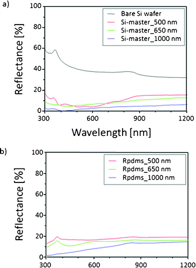 | ||
| Fig. 4 (a) The reflectance of the periodically textured Si-masters with three different profiles of the height in comparison with a bare Si wafer (black solid line) as a reference. (b) The reflectance of the negative semi-pyramid nanostructured PDMS AR layers with three different depth profiles of 500 nm, 650 nm, and 1000 nm, respectively. | ||
Conclusions
In this work, the periodically textured Si-masters with three different heights of 500 nm, 650 nm, and 1000 nm, respectively, were surface modified using organo-silane FOTS, and they showed dramatically enhanced hydrophobicity. The periodically textured Si-masters with a 500 nm height recorded a high contact angle of approximately 153°. This is an important issue in replication processes to decrease the adhesion force at the interface between the periodically textured Si-master and the imprinted PDMS AR layer for effective pattern transfer without any defects. Combined with enhanced surface hydrophobicity, the periodically textured Si-masters were used to transfer the patterns into PDMS layers using an imprinting-assisted replication processes. Finally, the introduced negative semi-pyramid nanostructure PDMS layers worked as anti-reflective surfaces and they showed significantly reduced reflectance of less than 20% over a broadband spectral wavelength ranging from 300 nm to 1200 nm. Therefore, the periodically textured Si-masters and their replicated negative semi-pyramid nanostructures in PDMS layers, which were fabricated and replicated by a simple manufacturing process with low cost, are promising for application in solar cells and photovoltaic cells to improve light conversion efficiency.References
- H. Xu, N. Lu, D. Qi, J. Hao, L. Gao, B. Zhang and L. Chi, Small, 2008, 4, 1972–1975 CrossRef CAS.
- C. Lee, S. Y. Bae, S. Mobasser and H. Manohara, Nano Lett., 2005, 5, 2438–2442 CrossRef CAS.
- M. M. Hasan, A. S. M. A. Haseeb, R. Saidur, H. H. Masjuki and M. R. Johan, AIP Conference Proceedings, 2009, 1136, 229–233 CrossRef CAS.
- J. Szczyrbowski, G. Bräuer, G. Teschner and A. Zmelty, J. Non-Cryst. Solids, 1997, 218, 25–29 CrossRef CAS.
- P. B. Clapham and M. C. Hutley, Nature, 1973, 244, 281–282 CrossRef.
- J. A. Hiller, J. D. Mendelsohn and M. F. Rubner, Nat. Mater., 2002, 1, 59–63 CrossRef CAS.
- M. Ibn-Elhaj and M. Schadt, Nature, 2001, 410, 796–799 CrossRef CAS.
- S. Walheim, E. Schäffer, J. Mlynek and U. Steiner, Science, 1999, 283, 520–522 CrossRef CAS.
- B. G. Prevo, E. W. Hon and O. D. Velev, J. Mater. Chem., 2007, 17, 791–799 RSC.
- J. Q. Xi, M. F. Schubert, J. K. Kim, E. F. Schubert, M. Chen, S.-Y. Lin, W. Liu and J. A. Smart, Nat. Photonics, 2007, 1, 176–179 CAS.
- Y. Kanamori, M. Sasaki and K. Hane, Opt. Lett., 1999, 24, 1422–1424 CrossRef CAS.
- C. Aydin, A. Zaslavsky, G. J. Sonek and J. Goldstein, Appl. Phys. Lett., 2002, 80, 2242–2244 CrossRef CAS.
- L. J. Guo, Adv. Mater., 2007, 19, 495–513 CrossRef CAS.
- J. Y. Kim, K.-S. Park, Z.-S. Kim, K.-H. Baek and L.-M. Do, Soft Matter, 2012, 8, 1184–1189 RSC.
- T. Senn, O. Kutz, C. Weniger, J. Li, M. Schoengen, H. Lochel, J. Wolf, P. Gottert and B. Lochel, J. Vac. Sci. Technol., B: Microelectron. Nanometer Struct.–Process., Meas., Phenom., 2011, 29, 061601–061605 CrossRef.
- D. Braha and A. Shmilovici, IEEE Trans. Semicond. Manuf., 2002, 15, 91–101 CrossRef.
- R. N. Wenzel, J. Phys. Colloid Chem., 1949, 53, 9 CrossRef.
- A. B. D. Cassie and S. Baxter, Trans. Faraday Soc., 1944, 40, 546–551 RSC.
- H. Zhao, K.-Y. Law and V. Sambhy, Langmuir, 2011, 27, 5927–5935 CrossRef CAS.
- X. Li, B. K. Tay, P. Miele, A. Brioude and D. Cornu, Appl. Surf. Sci., 2009, 255, 7147–7152 CrossRef CAS.
- Y. M. Song, J. H. Jang, J. C. Lee, E. K. Kang and Y. T. Lee, Sol. Energy Mater. Sol. Cells, 2012, 101, 73–78 CrossRef CAS.
- J. Y. Chen and K. W. Sun, Sol. Energy Mater. Sol. Cells, 2010, 94, 629–633 CrossRef CAS.
- D. Qi, N. Lu, H. Xu, B. Yang, C. Huang, M. Xu, L. Gao, Z. Wang and L. Chi, Langmuir, 2009, 25, 7769–7772 CrossRef CAS.
Footnotes |
| † Electronic supplementary information (ESI) available. See DOI: 10.1039/c2ra20771k |
| ‡ Jong-Chang Woo and Nam Seob Baek contributed equally to this work |
| This journal is © The Royal Society of Chemistry 2012 |