Facile synthesis of hierarchical Bi2S3 nanostructures for photodetector and gas sensor†
Haohua
Li
*a,
Juan
Yang
d,
Jianying
Zhang
c and
Ming
Zhou
*ab
aCenter for Photon Manufacturing Science and Technology, School of Materials Science and Engineering, Jiangsu University, Zhenjiang, 212013, PR China. E-mail: zm_laser@126.com; lihaohua@ujs.edu.cn; Fax: +86 51188791288; Tel: +86 51188791947
bThe State Key Laboratory of Tribology, Tsinghua University, Beijing, 10084, PR China. E-mail: zhouming@tsinghua.edu.cn; Fax: +86 1062781379; Tel: +861062783968
cFood Inspection Center, Shenzhen Entry–Exit Inspection and Quarantine Bureau, Shenzhen, 518045, PR China
dSchool of Materials Science and Engineering, Jiangsu University, Zhenjiang, 212013, PR China
First published on 13th June 2012
Abstract
The fabrication of a photodetector and gas sensor based on hierarchical Bi2S3 nanostructures is reported. Single crystalline Bi2S3 nanostructures with [001] growth direction were obtained via a facile hydrothermal method without any templates or surfactants. The photodetector showed steady photoresponses with a fast response time of ∼50 ms. Moreover, these Bi2S3 nanostructures exhibited a good sensing to methanol. These results show these hierarchical Bi2S3 nanostructures are promising candidates for constructing optoelectronic and gas sensing devices.
Introduction
Controllable synthesis of nanomaterials with specific morphology and structure has been a central subject of materials science, because their properties strongly depend on their size, shape and composition.1–3 Over the past few years, one-dimensional (1D) nanostructures, such as nanorods, nanotubes, nanowires and nanobelts, have attracted intensive interest due to their unique optical, electronic and mechanical properties, and potential application in the fabrication of nanoscale devices.4–6 Recently, considerable attention has been paid to the assembly of 1D nanostructures into hierarchical/super nanostructures. Compared with 1D nanostructures, complex nanostructures have larger surface areas and can form continuous networks, which further broaden their applications in sensors, catalysis, photovoltaic devices, and environmental protection.7–10 Up to now, several approaches including chemical vapor deposition,8 electrodeposition,10 hydrothermal and solvothermal methods7 have been reported for the synthesis of hierarchical nanostructures. Nevertheless, more facile and effective methods to fabricate hierarchical nanostructures are still highly desirable and challenging.Bi2S3, a narrow band gap semiconductor with band gap of 1.3–1.7 eV, has received intensive attention due to its wide application in electronic devices, optoelectronic devices, thermoelectric devices, hydrogen storage materials and sensors.11–16 In particular, Bi2S3 is considered as one of the most promising materials for photoactive materials due to its low band gap, high absorption coefficient and reasonable energy conversion efficiency (∼5%).17,18 As an efficient photoactive material, Bi2S3 should have a large surface area for photoreaction and high crystallinity for fast electron separation and transport.19 In this regard, Bi2S3 nanomaterials with hierarchical structure should be highly attractive and desirable as a photoactive material owing to their unique structure and high surface area. In order to achieve this purpose, much effort has been devoted to the fabrication of highly crystalline hierarchical Bi2S3 nanostructures with large surface area.20–24 Their outstanding properties make them very promising as functional building blocks for the fabrication of various nanodevices such as optoelectronic devices and gas sensors.25–27 However, to the best of our knowledge, optoelectronic devices and gas sensors based on hierarchical Bi2S3 nanostructures have not been reported, even though many hierarchical Bi2S3 nanostructures have been synthesized.20–24
In this paper, we report the synthesis of hierarchical Bi2S3 nanostructures via a facile low-temperature and surfactant-free hydrothermal method. Single crystalline hierarchical Bi2S3 nanostructures consisting of abundant 1D nanorods were obtained simply using Bi(NO3)3 and thiourea as starting materials. The photodetector based on hierarchical Bi2S3 nanostructures exhibited a clear photoresponse under sunlight. Moreover, we found that these Bi2S3 nanostructures showed a good sensing capability to methanol at low temperature. These findings indicate these hierarchical Bi2S3 nanostructures are promising candidates for building high performance optoelectronic and gas sensitive devices.
Results and discussion
The Bi2S3 product phase was identified by XRD and a typical XRD pattern is shown in Fig. 1a. All the diffraction peaks can be readily assigned to the orthorhombic phase of Bi2S3 (JCPDF card: 17-0320) with lattice constants a = 11.15 Å, b = 11.30 Å and c = 3.981 Å. The product is highly pure since no peaks of any impurity phase could be observed from this pattern. Furthermore, the intense and sharp peaks indicate that the product is well crystallized. Fig. S1 (ESI†) shows a typical low-magnification SEM image of the product prepared at 120 °C for 6 h. It is observed that large numbers of spherical urchin shape structures of Bi2S3 are obtained with size in the range of 2.5–4 μm. Fig. 1b and c show high-magnification SEM images of the product, clearly revealing each urchin-like Bi2S3 sphere is composed of many Bi2S3 nanorods with a diameter of about 60 nm and length of 1 μm. The Bi2S3 nanorods radiate from the center of the sphere so constituting a hierarchical Bi2S3 micro/nanostructure.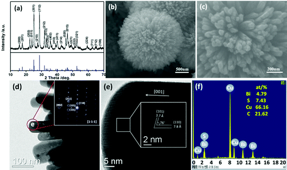 | ||
| Fig. 1 (a) XRD pattern, (b, c) SEM images, (d) TEM image, (e) HRTEM image and (f) EDS spectrum of hierarchical Bi2S3 nanostructures obtained at 120 °C. The inset in d is the corresponding SAED pattern. | ||
Fig. S2 (ESI†) shows the TEM image of an individual hierarchical Bi2S3 nanostructure with urchin-like morphology. The urchin-like Bi2S3 nanostructure is constructed by a large number of nanorods, and the typical diameter of these nanorods is 60 nm (Fig. 1d), corroborating the results by SEM. The corresponding selected-area electron diffraction (SAED) (inset of Fig. 1d) pattern reveals the nanorods exhibiting single-crystalline feature with a [001] growth direction. Fig. 1e is a HRTEM image of the circled area from Fig. 1d. Clear lattice fringes were observed, indicating this nanorod is single crystalline. In addition, the lattice fringes with a d-spacing of 7.8 and 3.7 Å can be well indexed to the (110) and (101) planes of orthorhombic Bi2S3, respectively. Also the angle between (110) and (101) planes is 76°, which is in agreement with the calculated value of 76.15°. Both the HRTEM observation and SAED analyses demonstrate that the Bi2S3 nanorods are single crystalline with a growth direction of [001]. Fig. 1f is the energy dispersive X-ray spectroscopy (EDS) pattern also obtained from the circled area of the nanorod in Fig. 1d. Besides the Cu and C signals from the TEM grid, only Bi and S are detected in the nanorod. Moreover, the atom ratio between Bi and S is close to 2![[thin space (1/6-em)]](https://www.rsc.org/images/entities/char_2009.gif) :3, which further demonstrated the nanorod is pure Bi2S3.
:3, which further demonstrated the nanorod is pure Bi2S3.
In order to further understand the composition and structure of these hierarchical Bi2S3 nanostructures, we preformed a Raman scattering measurement, and the typical Raman spectrum of the hierarchical Bi2S3 nanostructures is presented in Fig. 2a. Five obvious vibrational peaks at 69.7, 112.3, 182.6, 238.7 and 253.2 cm−1 were observed. The peaks at 112.3, 238.7 and 253.2 cm−1 accord well with the Raman bands reported previously28,29 while the peaks at 69.7 and 182.6 cm−1 may be attributed to surface phonon modes.30Fig. 2b shows the typical UV-visible absorption spectrum of the Bi2S3 nanostructures. It can be seen that there is a broad peak between 650 and 800 nm. Furthermore, the calculated direct bandgap of the Bi2S3 nanostructures is 1.67 eV (Fig. S3, ESI†).
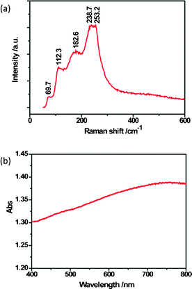 | ||
| Fig. 2 (a) Room-temperature Raman spectrum and (b) optical absorption spectrum of hierarchical Bi2S3 nanostructures. | ||
It is well known that nanomaterials with narrow band gap and high crystallinity can greatly improve the light harvesting capability, provide large surface area, shorten the diffusion path of current carriers, enhance the electron transport, and may have important potential application in photovoltaic devices. Therefore, we fabricated a simple photodetector based on these hierarchical Bi2S3 nanostructures to examine their photoconductive properties. Fig. 3a shows a schematic diagram of a photodetector based on hierarchical Bi2S3 nanostructures. The current–voltage (I–V) characteristics of the photodetector in the dark and with illumination of 100 mW cm−2 (AM 1.5) are recorded and presented in Fig. 3b. The linear behavior of the I–V curve under dark condition indicates that the silver/ITO electrodes and Bi2S3 have a good ohmic contact, and the resistance was calculated to be 456–543 MΩ. Upon light illumination, an obvious photoexcited current was observed, which demonstrates these hierarchical Bi2S3 nanostructures have excellent photovoltaic response under light illumination. Besides, the I–V curve remained linear, showing the high stability of the ohmic contact between silver electrodes and Bi2S3 nanostructures.
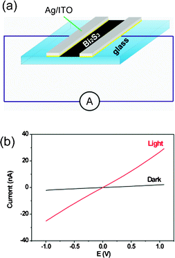 | ||
| Fig. 3 (a) Schematic diagram of the photodetector based on hierarchical Bi2S3 nanostructures. (b) Current–voltage (I–V) characteristics of the photodetector in the dark and with illumination of 100 mW cm−2 (AM 1.5). | ||
The stability and response capability of the photoactive materials are two of the most important factors for high-performance photoelectric devices. Herein, we preformed steady and transient state amperometric i–t measurements to test the stability of our photodetector. Fig. 4a illustrates the time-dependent photocurrent of this device measured at different bias potentials when the light source was switched on and off. It is clearly shown that the photocurrent is increased with increase in bias potential, suggesting the separation of photogenerated electrons and holes is more efficient at a high bias. Additionally, it is noted that the photocurrent quickly reaches steady state (the maximum value) under light illumination and quickly returned to normal state under light-off, revealing these hierarchical Bi2S3 nanostructures show very fast response to the light. For further understanding this fast response, the response and reset times of the device were also evaluated by measuring transient state amperometric i–t curves. Herein, the response time is defined as the time required for the photocurrent upon illumination to increase to 90% of the maximum photocurrent, while the recovery time is defined as the time needed to recover to 10% of the maximum photocurrent. From Fig. 4b and c, we find that the calculated response and recovery times for different bias potentials were very similar, and were 50 and 240 ms, respectively. These present values are comparable to those found for Bi2S3 core–shell microspheres,31 Bi2S3 nanotubes17 and Bi2S3 nanoparticles.17 All these results demonstrate that the present Bi2S3 photodetector has a good stability and fast response towards light.
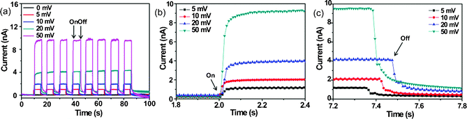 | ||
| Fig. 4 Current–time (i–t) characteristics: (a) switching, (b) off–on and (c) on–off light response of the hierarchical Bi2S3 nanostructures photodetector. | ||
Precise and economical monitoring of chemical gases is critical for human health, industrial processes and environmental considerations. Here, we also used a device to test the gas sensing properties of these Bi2S3 nanostructures. Fig. 5a shows a schematic image for methanol detection (methanol vapour produced from evaporating a methanol solution on a heating stage at 40 °C). Fig. 5b plots the change of current in the Bi2S3 nanostructures at 0.5 V bias as a function of time. It can be clearly seen that the current was increased two-fold when the device was in methanol gas atmosphere for 10 s and the current returned to the original state when the device was in air for 10 s. This current increase could be mainly attributed to the surface of these hierarchical Bi2S3 nanostructures absorbing large numbers of methanol gas molecules, resulting in a decrease of resistance, and hence improved conductivity of these Bi2S3 nanostructures. The complete recovery of the device in air is probably due to the reaction between O2 and methanol. Moreover, the above processes are reversible due to a displacement of physisorbed methanol molecules. Although the sensing measurement was preliminary the result demonstrates that the present sensor does show evident sensitivity towards methanol and suggests that these Bi2S3 nanostructures may have potential in gas sensor applications.
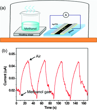 | ||
| Fig. 5 (a) Schematic illustration of methanol detection and (b) current variation of the gas sensor based on hierarchical Bi2S3 nanostructures at 0.5 V bias as a function of time. | ||
Conclusions
In summary, single-crystalline hierarchical Bi2S3 nanostructures were successfully prepared via a one-pot hydrothermal process. A photodetector and a gas sensor based on these hierarchical Bi2S3 nanostructures were constructed to study their photoconductive and gas sensing properties. The photoconductive measurements demonstrate that these Bi2S3 nanostructures show an excellent stability and fast response towards light. Gas detection studies show these Bi2S3 nanostructures have a good sensitivity to methanol at room temperature. These findings indicate these hierarchical Bi2S3 nanostructures may have great potential applications in constructing high-performance optoelectronic devices and gas sensors.Acknowledgements
This Research was supported by the National Basic Research Program of China (973 Program, Grant No.2011CB013004), the Nature Science Foundation of China (Grant No. 50975129, 50902061), Major Project of State Key Laboratory of Tribology (Grant No.SKLT10A02), Senior Intellectuals Fund of Jiangsu University (Grant No.11JDG100) and the Project Funded by the Priority Academic Program Development of Jiangsu Higher Education Institutions (PAPD).References
- X. H. Lu, D. Z. Zheng, T. Zhai, Z. Q. Liu, Y. Y. Huang, S. L. Xie and Y. X. Tong, Energy Environ. Sci., 2011, 4, 2915–2921 CAS.
- G. M. Wang, Y. C. Ling, H. Y. Wang, X. Y. Yang, C. C. Wang, J. Z. Zhang and Y. Li, Energy Environ. Sci., 2012, 5, 6180–6187 CAS.
- T. Zhai, S. L. Xie, Y. F. Zhao, X. F. Sun, X. H. Lu, M. H. Yu, M. Xu, F. M. Xiao and Y. X. Tong, CrystEngComm, 2012, 14, 1850–1855 RSC.
- X. H. Lu, T. Zhai, X. H. Zhang, Y. Q. Shen, L. Y. Yuan, B. Hu, L. Gong, J. Chen, Y. H. Gao, J. Zhou, Y. X. Tong and Z. L. Wang, Adv. Mater., 2012, 24, 938–944 CrossRef CAS.
- X. H. Lu, G. M. Wang, T. Zhai, M. H. Yu, J. Y. Gan, Y. X. Tong and Y. Li, Nano Lett., 2012, 12, 1690–1696 CrossRef CAS.
- G. M. Wang, H. Y. Wang, Y. C. Ling, Y. C. Tang, X. Y. Yang, R. C. Fitzmorris, C. C. Wang, J. Z. Zhang and Y. Li, Nano Lett., 2011, 11, 3026–3033 CrossRef CAS.
- Z. H. Zhang and P. Wang, Energy Environ. Sci., 2012, 5, 6067–6071 Search PubMed.
- X. H. Zhang, X. H. Lu, Y. Q. Shen, J. B. Han, L. Y. Yuan, L. Gong, Z. Xu, X. D. Bai, M. Wei, Y. X. Tong, Y. H. Gao, J. Chen, J. Zhou and Z. L. Wang, Chem. Commun., 2011, 47, 5804–5806 RSC.
- Q. Tang, Z. Y. Lu, Z. Chang, W. Zhu, J. Q. Sun, J. F. Liu, X. M. Sun and X. Duan, RSC Adv., 2012, 2, 1663–1668 RSC.
- X. H. Lu, D. Wang, Gao-Ren Li, C. Y. Su, D. B. Kuang and Y. X. Tong, J. Phys. Chem. C, 2009, 113, 13574–13582 CAS.
- Z. H. Ge, B. P. Zhang, Z. X. Yu and B. B. Jiang, CrystEngComm, 2012, 14, 2283–2288 RSC.
- J. M. Ma, Z. F. Liu, J. B. Lian, X. C. Duan, T. L. Kim, P. Peng, X. D. Liu, Q. Chen, G. Yao and W. J. Zheng, CrystEngComm, 2011, 13, 3072–3079 RSC.
- J. M. Ma, J. Q. Yang, L. F. Jiao, T. H. Wang, J. B. Lian, X. C. Duan and W. J. Zheng, Dalton Trans., 2011, 40, 10100–10108 RSC.
- L. Cademartiri, R. Malakooti, P. G. O. Brien, A. Migliori, S. Petrov, N. P. Kherani and G. A. Ozin, Angew. Chem., Int. Ed., 2008, 47, 3814–3817 CrossRef CAS.
- Z. W. Quan, J. Yuan, P. P. Yang, Z. L. Wang, X. C. Li and J. Lin, Cryst. Growth Des., 2008, 8, 200–207 CAS.
- C. X. Song, D. B. Wang, T. Yang and Z. S. Hu, CrystEngComm, 2011, 13, 3087–3092 RSC.
- A. A. Tahir, M. A. Ehsan, M. Mazhar, K. G. U. Wijayantha, M. Zeller and A. D. Hunter, Chem. Mater., 2010, 22, 5084–5092 CrossRef CAS.
- L. M. Peter, K. G. U. Wijayantha, D. J. Riley and J. P. Waggett, J. Phys. Chem. B, 2003, 107, 8378–8381 CrossRef CAS.
- L. Martinez, M. Bernechea, F. P. De-Arquer and G. Konstantatos, Adv. Energy Mater., 2011, 1, 1029–1035 CrossRef CAS.
- H. Bao, C. M. Li, X. Cui, Q. Song, H. Yang and J. Guo, Nanotechnology, 2008, 19, 335302 CrossRef.
- Y. Zhao, Y. Xie, J. S. Jie, C. Y. Wu and S. Yan, J. Mater. Chem., 2009, 19, 3378–3383 RSC.
- X. D. Zhou, H. Q. Shi, B. Zhang, X. Fu and K. Jiao, Mater. Lett., 2008, 62, 3201–3204 CrossRef CAS.
- C. J. Tang, C. Q. Wang, F. J. Su, C. H. Zang, Y. X. Yang, Z. J. Zong and Y. S. Zhang, Solid State Sci., 2010, 12, 1352–1356 CrossRef CAS.
- H. Y. Zhou, S. L. Xiong, L. Z. Wei, B. J. Xi, Y. C. Zhu and Y. T. Qian, Cryst. Growth Des., 2009, 9, 3862–3867 CAS.
- G. Konstantatos, L. Levina, J. Tang and E. H. Sargent, Nano Lett., 2008, 8, 4002–4006 CrossRef CAS.
- X. L. Yu and C. B. Cao, Cryst. Growth Des., 2008, 8, 3951–3955 CAS.
- K. Yao, W. W. Gong, Y. F. Hu, X. L. Liang, Q. Chen and L. M. Peng, J. Phys. Chem. C, 2008, 112, 8721–8724 CAS.
- Y. Wee Koh, C. S. Lai, A. Y.n Du, E. R. T. Tiekink and K. P. Loh, Chem. Mater., 2003, 15, 4544–4554 CrossRef.
- X. H. Yang, X. Wang and Z. D. Zhang, Mater. Chem. Phys., 2006, 95, 154–157 CrossRef CAS.
- S. Y. Wang and Y. W. Du, J. Cryst. Growth, 2002, 236, 627–634 CrossRef CAS.
- S. S. Li, R. G. Cao, Z. J. Wang, J. J. Li and L. Q. Qi, J. Phys. Chem. C, 2009, 113, 18075–18081 Search PubMed.
Footnote |
| † Electronic supplementary information (ESI) available: Detailed experimental section. SEM and TEM images of hierarchical Bi2S3 nanostructures. See DOI: 10.1039/c2ra20751f |
| This journal is © The Royal Society of Chemistry 2012 |