Achieving chemical stability in thermoelectric NaxCoO2 thin films
P.
Brinks
,
H.
Heijmerikx
,
T. A.
Hendriks
,
G.
Rijnders
and
M.
Huijben
*
Faculty of Science and Technology and MESA+ Institute for Nanotechnology, University of Twente, P.O. Box 217, 7500 AE, Enschede, The Netherlands. E-mail: m.huijben@utwente.nl
First published on 30th May 2012
Abstract
Stability issues in thermoelectric NaxCoO2 thin films have been solved by the addition of an in situ amorphous AlOx capping layer, which prevents previously reported degradation when exposed to air. These chemically stable thin films enable detailed analysis of the intrinsic thermoelectric properties and form a significant progress towards applications. Single phase NaxCoO2 thin films with a low surface roughness are grown by pulsed laser deposition with either an epitaxial or textured crystal structure on Al2O3(001) or LaAlO3(001) single crystal substrates, respectively. For textured thin films a resistivity and thermopower of 0.99 mΩ cm and 69 μV K−1 are observed at room temperature, respectively. Based on an estimated thermal conductivity for thin films, the dimensionless figure of merit is very comparable to NaxCoO2 single crystals, demonstrating the effectiveness of the developed capping layer.
1 Introduction
A large rise in research on thermoelectric power generation is currently occurring because of the improved properties of various nanostructured thermoelectric materials.1 These improved materials make the recovery of the waste heat emitted by vehicles and factories, but also electronic processors, more attractive and economically feasible. Due to a difference of several orders of magnitude in the surface to volume ratio for nanostructured materials compared to their bulk counterparts, the reactivity and high temperature stability is significantly different and a detailed knowledge about the long-term stability of these new thermoelectric materials is required. The observation of a high thermopower and low resistivity in NaxCoO2 single crystals2 opened up the interest in them as promising thermoelectric candidate materials3–7 and figure of merit (ZT) values exceeding unity have already been achieved. The efficiency of a material for thermoelectric power generation is given by the dimensionless figure of merit ZT: | (1) |
The improvement achieved by using nanostructured materials is caused by the enhanced phonon scattering within these nano structures. This leads to a reduction of the thermal conductivity, without affecting the electronic properties, and thereby results in an improved ZT value. One of the approaches towards these nanostructured materials is to design superlattice structures in thermoelectric thin films, which will enhance the phonon scattering because of the low-dimensional confinement between the interfaces. This approach has been theoretically predicted12 and experimentally demonstrated13 for Bi2Te3-based materials. In oxide thermoelectric materials the initial thermal conductivity is even larger, and therefore the enhancement of phonon scattering by superlattice design could lead to an even stronger reduction of the thermal conductivity. Thin films of NaxCoO2 could serve as the building blocks for such superlattice structures and have already been investigated in previous studies.14–19 However, no detailed analysis of the thermoelectric properties of these thin films has been performed to date, due to chemical instability of the thin films at ambient conditions.14
Here, we present a method to obtain single phase thin films of NaxCoO2, which are chemically stable in ambient conditions. By the in situ deposition of an AlOx capping layer on top of the thin films direct contact to moisture and CO2 is prevented and the reactive nature of the NaxCoO2 layer can be suppressed. This enables us to study for the first time in detail the relationship between structural and thermoelectric properties, i.e. electrical transport and room temperature thermopower in chemically stable NaxCoO2 thin films on different single crystal substrates. We will demonstrate that NaxCoO2 thin films possess comparable thermoelectric behavior to their single crystal analogues.
2 Experimental methods
Thin film samples of NaxCoO2 were fabricated by pulsed laser deposition (PLD) on single crystal (001)-oriented Al2O3 and (001)-oriented LaAlO3 substrates, which are promising substrate candidates.14–19 Before deposition, the substrates were annealed for 1 h at 1050 °C (Al2O3) and at 950 °C with an oxygen flow of 150 ml min−1 (LaAlO3), exhibiting smooth surfaces with clear unit-cell-height steps with atomic force microscopy (AFM). The low level of surface roughness after annealing can be seen in Fig. 1a and Fig. 1d for a typical annealed Al2O3 and LaAlO3 substrate, respectively. A sintered target with the composition Na0.9CoO2 was chosen as it is predicted to have the best thermoelectric properties,20 which were also demonstrated experimentally in single crystals.11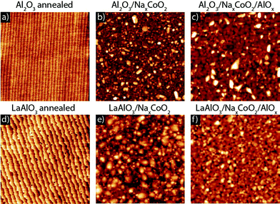 | ||
| Fig. 1 Atomic force microscopy images (3 × 3 μm2) of annealed Al2O3 and LaAlO3 substrates (a and d), after growth of a 60 nm NaxCoO2 thin film (b and e) and after growth of an additional 80 nm amorphous AlOx capping layer (c and f). | ||
Thin NaxCoO2 films were deposited with a laser fluence of ∼4 J cm−2, a spotsize of ∼1.08 mm2 and a repetition rate of 1 Hz. These laser settings resulted in single phase thin films, whereas at higher laser repetition rates impurity phases were formed. During growth the oxygen environment was kept at ∼0.4 mbar. After the growth the samples were slowly cooled to room temperature in 1 atm of oxygen at a rate of 10 °C min−1 to optimize the oxidation level. In order to improve the chemical stability of the thin films, we added an amorphous AlOx capping layer in situ to several NaxCoO2 thin films. These amorphous AlOx layers were grown at room temperature in ∼5 × 10⁻³ mbar of oxygen, from a polycrystalline Al2O3 target. AFM analysis demonstrates a surface topography of the thin films with low roughness (RMS: ∼4 nm) independent of the presence of the amorphous (AlOx) capping layer, see Fig. 1. Gold contacts were deposited to establish good ohmic contact to the NaxCoO2 layer for thermoelectric characterization.
3 Results and discussion
3.1 Structural characterization
The structural properties of the thin films were determined by X-ray diffraction. A typical 2θ/ω scan for a 60 nm thin NaxCoO2 film, deposited at 430 °C, is shown in Fig. 2 when grown on an Al2O3 and a LaAlO3 substrate. Both thin films exhibit only (00l) peaks of NaxCoO2 indicating a preferred growth orientation with the c-axis of the thin film and the substrate aligned parallel to each other. The c-axis lattice parameters are 10.95 ± 0.05 Å and 11.05 ± 0.05 Å for samples deposited on Al2O3 and LaAlO3 substrates, respectively. Since no impurity peaks are observed it is concluded that the films are single-phase.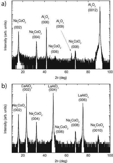 | ||
| Fig. 2 X-Ray diffraction spectra for 60 nm NaxCoO2 thin films deposited on single crystal Al2O3 (a) and LaAlO3 (b) substrates. Only (00l) peaks of the thin films are observed, indicating that the films are single phase and exhibit a preferred growth orientation. | ||
Even though the growth orientation is similar for the thin films grown on these two different substrates, for the in-plane direction clear differences are observed. For thin films grown on Al2O3 substrates an in-plane epitaxial relationship is found between the substrate and the thin film. The hexagonal structure of the NaxCoO2 is rotated by 30° with respect to that of the substrate. This is demonstrated in Fig. 3 where it is shown that in a ϕ scan the peak positions of the (104) peak of the substrate are found to match that of the (112) film peak. The a-axis lattice parameter is 2.82 Å for these epitaxial thin films. For the LaAlO3 substrate no in-plane epitaxial relationship between the substrate and the thin film was found, therefore indicating that the samples were textured. Although a large lattice mismatch exists for both substrate materials, the different crystal structure of these substrates, hexagonal21 (Al2O3) and cubic22 (LaAlO3), enables the growth of either epitaxial or textured NaxCoO2 thin films.
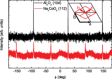 | ||
| Fig. 3 X-Ray diffraction measurements demonstrating the epitaxial relationship between the Al2O3 substrate and the NaxCoO2 thin film. The ϕ positions of the (112) and (104) peaks of the thin film and substrate, respectively, indicate the rotation of the a-axis of the film by 30° compared to the substrate as schematically shown. | ||
In contrast to previous reports on the narrow range of deposition temperatures for the growth of single-phase thin films,14 we observed a much wider range (330 °C–650 °C) for our deposition conditions. Fig. 4 shows a clear difference in the crystallinity for NaxCoO2 thin films grown on LaAlO3 substrates at various deposition temperatures. Due to the volatility of sodium, it is expected that the sodium concentration within the sample is dependent on the deposition temperature.15 Therefore, a change in sodium concentration as a function of deposition temperature could lead to a corresponding change in the c-axis length of the NaxCoO2 unit cell.23,24 However, the observed peak shift is relatively small, as can be seen in Fig. 4, and a c-axis lattice parameter of 11.05 ± 0.05 Å was determined for these samples. Based on these results it is concluded that the sample stoichiometry is constant for this range of deposition temperatures.
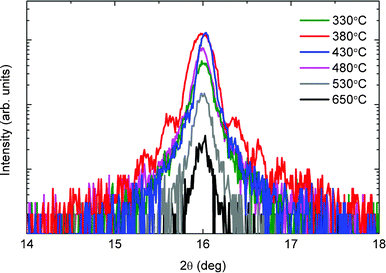 | ||
| Fig. 4 X-Ray diffraction measurements of the (002) peak of the NaxCoO2 thin film on LaAlO3 substrates at varying deposition temperatures. Only small peak shifts are observed, indicating minimal variation in the sample stoichiometry. | ||
3.2 Chemical stability
The electrical transport properties of thin NaxCoO2 films are known to degrade with time in ambient conditions.14 We indeed observed a strong increase in resistance for NaxCoO2 thin films, see Fig. 5. For the epitaxial and textured films an increase of resistance by a factor of 2.2 and 50, respectively, is observed over a period of two days, after which it stabilizes. The degradation can be interrupted by placing the sample in a vacuum environment (10−5 mbar), while subsequent exposure to ambient conditions continues the degradation process. These stability issues have previously hampered accurate analysis of the thermoelectric properties of NaxCoO2 thin films.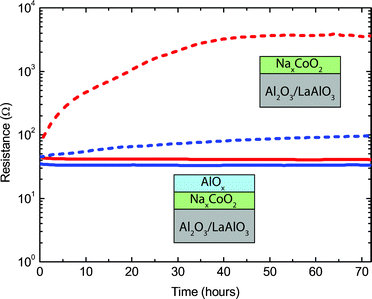 | ||
| Fig. 5 Time-dependent resistance measurements of NaxCoO2 thin films on Al2O3 (blue) and LaAlO3 (red) single crystal substrates at 300 K. Measurements are shown for samples with (solid lines) and without (dashed lines) an AlOx capping layer. | ||
A reaction of sodium from the sample with moisture and carbon dioxide from the air has been suggested to occur,14 which leads to the formation of sodium carbonate (Na2CO3). However, after exposing the samples to ambient conditions for several days, no significant change in the XRD spectra is observed, indicating that a large volume fraction is not influenced by these reactions. From these observations it is concluded that only the surface layer and the grain boundaries are sensitive to the exposure to ambient conditions. To verify the formation of Na2CO3 at the surface, X-ray photoelectron spectroscopy (XPS) measurements were performed on a thin film, which had been transferred into the XPS chamber immediately after deposition. During the sample transfer from PLD to XPS the sample was exposed to ambient conditions for a short time, during which some Na2CO3 had already been formed. This was indeed confirmed by XPS analysis, where for carbon 1s a double peak was observed. One of these peaks was identified as a carbonate peak. No change in the XPS spectrum was observed after storage in an ultra-high vacuum for one week. However, after exposure to ambient conditions for several days, a clear increase in the carbon 1 s peak, originating from the carbonate impurity phase, was measured. Indicating that the formation of carbonate at the surface and grain boundaries is indeed a process taking place due to the exposure to ambient conditions. This has a dramatic effect on the electrical transport going through the degrading grain boundaries as shown in Fig. 5. The degradation process is significantly stronger for textured films, which can be explained by the misalignment of the grains for the in-plane direction.
In order to prevent the formation of sodium carbonate at the surface and grain boundaries a capping layer was developed. The in situ deposition of such a protective capping layer is a favorable solution to avoid any exposure to ambient conditions. A good candidate material is Al2O3, since it has been used previously as a diffusion barrier25 and it can be deposited by PLD in either polycrystalline or amorphous layers. For polycrystalline capping layers of Al2O3 only a small improvement in the stability was observed, which is most likely caused by an incomplete coverage due to island formation of the polycrystalline capping layer. However, a fully closed coverage of the surface can be expected for an amorphous AlOx layer.26 This was indeed confirmed by AFM for an AlOx capping layer deposited at room temperature and at an oxygen pressure of 5 × 10⁻³ mbar. Deposition of AlOx at higher oxygen pressures resulted in an increased surface roughness and, therefore, a reduced surface coverage. The surface topography of samples with an additional 80 nm amorphous AlOx capping layer is shown in Fig. 1c and Fig. 1f for NaxCoO2 thin films on Al2O3 and LaAlO3 substrates, respectively. This thickness was used to ensure a complete coverage of all the trenches and islands present at the NaxCoO2 surface. For both samples the RMS-value of the surface roughness is ∼4 nm and is comparable to samples without a capping layer. Detailed analysis of the electrical transport properties showed that the implementation of an additional amorphous AlOx capping layer completely prevented any degradation in ambient conditions for epitaxial and textured thin films, see Fig. 5. Reference samples where only the AlOx capping layer was deposited were electrically insulating, ensuring that the measured behavior was only from the NaxCoO2 thin film. The AlOx-capped samples remain stable over a period of several months and this enables us to study for the first time in detail the relationship between structural and thermoelectric properties in chemically stable NaxCoO2 thin films on different single crystal substrates.
3.3 Thermoelectric characterization
The thermoelectric properties of AlOx-capped NaxCoO2 thin films are determined and compared to reported single crystal values. The temperature dependence of the electrical transport properties are measured in the range 4–300 K and shown in Fig. 6. The analysis is given for two samples which are deposited at 430 °C and 0.4 mbar on Al2O3 and LaAlO3 substrates, respectively. These two samples represent typical results for thin films grown on these two substrates and show interesting differences which can be explained by their crystallographic properties. A lower resistivity is observed for the sample deposited on Al2O3, compared to the sample deposited on LaAlO3. Since the carrier densities are comparable, the change in resistivity is caused by variations in the carrier mobility. This difference in the carrier mobility can be explained by the crystallographic orientations of the grains within the thin films. Both samples have a parallel alignment of the c-axis in all grains. Additionally, the sample deposited on the Al2O3 substrate possesses grains, which are also in-plane aligned with respect to the substrate. This additional in-plane alignment leads to an enhanced carrier mobility, as electron scattering is reduced.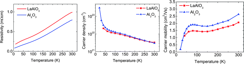 | ||
| Fig. 6 The temperature dependence of resistivity, carrier density and carrier mobility for AlOx-capped NaxCoO2 thin films on Al2O3 (blue triangles) and LaAlO3 (red squares) substrates. | ||
The observed metallic behavior down to low temperatures is in good agreement with previously reported single crystals. However, previous studies reported values for the room temperature resistivity of NaxCoO2 single crystals with a stoichiometry of x = 0.8–0.95 between 1.5 and 22 mΩ cm,6,11,27 while our thin films exhibit significantly lower values of 0.79 and 0.99 mΩ cm for growth on Al2O3 and LaAlO3 substrates, respectively. Additionally, the measured carrier density at room temperature of ∼3 × 1021 cm−3 for our thin films is more than 2 orders of magnitude larger than the values observed for Na0.9CoO2 single crystals.6 Also a small increase in the carrier density at lower temperatures was reported for Na0.9CoO2 single crystals, in contrast to the strong observed enhancement for our thin films.
Comparing the transport properties of our thin films with NaxCoO2 single crystals with different compositions, a remarkable similarity is observed for Na0.68CoO2 single crystals.28 For these single crystals a room temperature carrier density of ∼1.8 × 1021 cm−3 is measured, which strongly increases upon cooling. This is in good agreement with our observations. Additionally, the observed room temperature resistivity of ∼0.8 mΩ cm is very similar to our thin films. It cannot be excluded that our thin films are composed of a sodium rich amorphous phase together with a crystalline phase with a stoichiometry close to Na0.68CoO2.
The measured thermopower at room temperature is ∼45 μV K−1 and ∼69 μV K−1 for thin films grown on Al2O3 and LaAlO3 substrates, respectively, which is very similar to single crystals with a composition close to Na0.71CoO2,11 see Table 1. Since the carrier density for these thin films is comparable, the difference in the thermopower is dominated by the carrier mobility with the highest thermopower observed for the thin film with the lowest mobility. This is in good agreement with the initial observation of the unusual combination of a high carrier density, low carrier mobility and high thermopower for single crystal NaxCoO2.2
| Al2O3 | LaAlO3 | Single crystal11 | |
|---|---|---|---|
| Resistivity (mΩ cm) | 0.79 | 0.99 | 1 |
| Thermopower (μV K−1) | 45 | 69 | 90 |
| Power Factor (μW K−2 cm−1) | 2.6 | 4.8 | 8.1 |
| Thermal conductivity (W mK−1) | 4 | 4 | 8 |
| ZT | 0.01 | 0.03 | 0.03 |
A power factor of 2.6 and 4.8 μW K−2 cm−1 is determined at room temperature for thin films on Al2O3 and LaAlO3 substrates, respectively. Even though the thermal conductivity of the thin films was not measured yet, a ZT value can be calculated based on an estimated value for the thermal conductivity. For single crystals a thermal conductivity between 8 and 19 W mK−1 is reported,9–11 which can only be obtained in the case of highly controlled growth with a very low defect density. Therefore, it can be expected that the thermal conductivity in thin films is substantially lower than for single crystal values. For an estimated thermal conductivity of 4 W mK−1, ZT values of 0.01 and 0.03 are obtained at room temperature for thin films on Al2O3 and LaAlO3 substrates, respectively, which are in very good agreement with reports on Na0.71CoO2 single crystals,11 see Table 1.
4 Conclusions
In summary, we have developed a method to obtain single phase thin films of NaxCoO2 which are stable in ambient conditions, due to the in situ deposition of an amorphous AlOx capping layer. Depending on the choice of the single crystal substrate, the thin films can be grown either epitaxial or textured. Although the power factor is lower than that of the NaxCoO2 single crystals, the thermal conductivity is also expected to be lower for these thin films. The ZT values of the NaxCoO2 thin films at room temperature are therefore comparable to that of the Na0.71CoO2 single crystals. These capped thin films enable the detailed study of the thermoelectric properties of NaxCoO2 and could open up new ways to maximize the ZT values. However, additional characterization of the thermoelectric properties at higher temperatures is required, since this is the most promising regime for future applications of thermoelectric oxide materials.Acknowledgements
We acknowledge B. Kuiper for XPS measurements. This work was supported by the Netherlands Organization for Scientific Research (NWO) through a VENI grant (M.H.).References
- B. C. Sales, Science, 2002, 295, 1248–1249 CrossRef CAS.
- I. Terasaki, Y. Sasago and K. Uchinokura, Phys. Rev. B, 1997, 56, R12685–R12687 CrossRef CAS.
- R. Funahashi, I. Matsubara, H. Ikuta, T. Takeuchi, U. Mizutani and S. Sodeoka, Jpn. J. Appl. Phys., 2000, 39, L1127–L1129 CAS.
- K. Fujita, T. Mochida and K. Nakamura, Jpn. J. Appl. Phys., 2001, 40, 4644–4647 CrossRef CAS.
- T. Motohashi, E. Naujalis, R. Ueda, K. Isawa, M. Karppinen and H. Yamauchi, Appl. Phys. Lett., 2001, 79, 1480–1482 CrossRef CAS.
- M. Mikami, M. Yoshimura, Y. Mori, T. Sasaki, R. Funahashi and M. Shikano, Jpn. J. Appl. Phys., 2003, 42, 7383–7386 CrossRef CAS.
- M. Lee, L. Viciu, L. Li, Y. Wang, M. L. Foo, S. Watauchi, R. A. Pascal Jr., R. J. Cava and N. P. Ong, Nat. Mater., 2006, 5, 537–540 CrossRef CAS.
- T. Caillat, M. Carle, P. Pierrat and S. Scherrer, J. Phys. Chem. Solids, 1992, 53, 1121–1129 CrossRef CAS.
- B. C. Sales, R. Jin, K. A. Affholter, P. Khalifah, G. M. Veith and D. Mandrus, Phys. Rev. B, 2004, 70, 174419 CrossRef.
- X. Tang and T. M. Tritt, J. S. C. Acad. Sci., 2008, 6, 10–13 Search PubMed.
- M. Lee, L. Viciu, L. Li, Y. Wang, M. L. Foo, S. Watauchi, R. A. Pascal Jr., R. J. Cava and N. P. Ong, Phys. B, 2008, 403, 1564–1568 CrossRef CAS.
- L. D. Hicks and M. S. Dresselhaus, Phys. Rev. B, 1993, 47, 12727–12731 CrossRef CAS.
- R. Venkatasubramanian, E. Siivola, T. Colpitts and B. O'Quinn, Nature, 2001, 413, 597–602 CrossRef CAS.
- H. Zhou, X. P. Zhang, B. T. Xie, Y. S. Xiao, C. X. Yang, Y. J. He and Y. G. Zhao, Thin Solid Films, 2006, 497, 338–340 CrossRef CAS.
- X. P. Zhang, Y. S. Xiao, H. Zhou, B. T. Xie, C. X. Yang and Y. G. Zhao, Mater. Sci. Forum, 2005, 3807, 475–479 Search PubMed.
- J. Y. Son, B. G. Kim and J. H. Cho, Appl. Phys. Lett., 2005, 86, 221918 CrossRef.
- Y. Krockenberger, I. Fritsch, G. Cristiani, A. Matveev, L. Alff, H. U. Habermeier and B. Keimer, Appl. Phys. Lett., 2005, 86, 191913 CrossRef.
- A. Venimadhav, A. Soukiassian, D. A. Tenne, Q. Li, X. X. Xi, D. G. Schlom, R. Arroyave, Z. K. Liu, H. P. Sun, X. Pan, M. Lee and N. P. Ong, Appl. Phys. Lett., 2005, 87, 172104 CrossRef.
- L. Yu, L. Gu, Y. Wang, P. X. Zhang and H. U. Habermeier, J. Cryst. Growth, 2011, 328, 34–38 CrossRef CAS.
- S. Mukerjee and J. E. Moore, Appl. Phys. Lett., 2007, 90, 112107 CrossRef.
- W. E. Lee and K. P. D. Lagerlof, J. Electron Microsc. Tech., 1985, 2, 247–258 CrossRef CAS.
- S. A. Hayward, F. D. Morrison, S. A. T. Redfern, E. K. H. Salje, J. F. Scott, K. S. Knight, S. Tarantino, A. M. Glazer, V. Shuvaeva, P. Daniel, M. Zhang and M. A. Carpenter, Phys. Rev. B, 2005, 72, 054110 CrossRef.
- Q. Huang, M. L. Foo, R. A. Pascal Jr., J. W. Lynn, B. H. Toby, H. Tao, H. W. Zandbergen and R. J. Cava, Phys. Rev. B, 2004, 70, 134115 CrossRef.
- Y. Krockenberger, I. Fritsch, G. Christiani, H. U. Habermeier, L. Yu, C. Bernhard, B. Keimer and L. Alff, Appl. Phys. Lett., 2006, 88, 162501 CrossRef.
- S.-H. Kim, C.-E. Kim and Y.-J. Oh, Thin Solid Films, 1997, 305, 312–326 Search PubMed.
- F. Di Fonzo, D. Tonini, A. Li Bassi, C. S. Casari, M. G. Beghi, C. E. Bottani, D. Gastaldi, P. Vena and R. Contro, Appl. Phys. A, 2008, 93, 765–769 CrossRef CAS.
- T. Ikeda and M. Onoda, J. Phys.: Condens. Matter, 2006, 18, 8673–8682 CrossRef CAS.
- M. Lin Foo, Y. Wang, S. Watauchi, H. W. Zandbergen, T. He, R. J. Cava and N. P. Ong, Phys. Rev. Lett., 2004, 92, 247001 CrossRef.
| This journal is © The Royal Society of Chemistry 2012 |