VO2 (A) nanostructures with controllable feature sizes and giant aspect ratios: one-step hydrothermal synthesis and lithium-ion battery performance†
Lei
Dai
a,
Yanfeng
Gao
*a,
Chuanxiang
Cao
a,
Zhang
Chen
a,
Hongjie
Luo
b,
Minoru
Kanehira
a,
Jun
Jin
b and
Yu
Liu
b
aState Key Laboratory of High Performance Ceramics and Superfine Microstructure, Shanghai institute of Ceramics, Chinese Academy of Sciences, Shanghai 200050, P. R. China. E-mail: yfgao@mail.sic.ac.cn; Fax: +86-21-6990-6218
bShanghai Institute of Ceramics (SIC), Chinese Academy of Sciences (CAS), Chengbei Road 215, Jiading, Shanghai, 201800, P. R. China
First published on 11th April 2012
Abstract
In this paper, uniform 1D VO2 (A) nanostructures with controllable morphologies were prepared via an easy one-step hydrothermal method for the first time. Aspect ratios are tunable from 10![[thin space (1/6-em)]](https://www.rsc.org/images/entities/char_2009.gif) :1 to 1000:1 by changing the synthesis parameters such as the concentration of vanadium source and the reaction time. The mechanism of morphology evolution was investigated and discussed based on the nucleation and growth process of VO2 (A) particles. Electrochemical analyses of VO2 (A) nanostructures were performed, and the results showed a capacity of 277 mAh g−1 for a Li-ion battery using these nanostructures as cathode materials. This shows a significant improvement compared with other vanadium oxides such as VO2 (B) (approximately 180 mAh g−1) and V2O5 (approximately 230 mAh g−1). Unfortunately, the VO2 (A) nanostructures exhibit high initial irreversible loss due to the formation of an intermediate layer after electrochemical reactions.
:1 to 1000:1 by changing the synthesis parameters such as the concentration of vanadium source and the reaction time. The mechanism of morphology evolution was investigated and discussed based on the nucleation and growth process of VO2 (A) particles. Electrochemical analyses of VO2 (A) nanostructures were performed, and the results showed a capacity of 277 mAh g−1 for a Li-ion battery using these nanostructures as cathode materials. This shows a significant improvement compared with other vanadium oxides such as VO2 (B) (approximately 180 mAh g−1) and V2O5 (approximately 230 mAh g−1). Unfortunately, the VO2 (A) nanostructures exhibit high initial irreversible loss due to the formation of an intermediate layer after electrochemical reactions.
Introduction
Due to the worldwide growing energy crisis, energy storage is more important today than ever before. Rechargeable lithium-ion batteries (LIBs) are a good choice for energy storage.1–3 Currently, the LIBs have powered hybrid electric vehicles and most modern portable electronic devices such as computers, cell phones, and cameras.4 However, in order to develop financially marketable, high-quality LIBs for a potentially massive market, further developments in safety, capacity, charge/discharge rates, and service life are still required.5,6 Among the components required of a battery containing a cathode, anode and electrolyte, the quality of the cathode material which concurrently stores electrons and Li+ is the bottleneck of LIB's performances. The exploration of novel materials and technological solutions are two major research focal points.7,8Most cathode materials used in LIBs have a layered structure. Vanadium oxide,9–17 especially V2O5,11–16 has been studied as a cathode material for decades,18 namely due to its high energy-density (the theoretical capacity can reach 440 mAh g−1 by inserting 3 Li+ in one molecular V2O5) and low cost.19 The layered structure of V2O5 is comprised of corner sharing VO5 square pyramids which form a sheet (Fig. 1a). This structure provides a variety of sites that are available for lithium intercalation. However, the low diffusion coefficient of lithium ions (D∼10−12 cm2 s−1),20 poor electrical conductivity (10−2 to 10−3 S cm−1)21 and limited cycling stability22 of vanadium pentoxide electrodes hinder the practical application of this material.
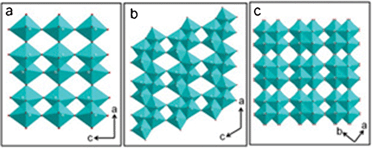 | ||
| Fig. 1 (a) The crystal structure of V2O5 projected along the b-axis; (b) the crystal structure of VO2 (B) projected along the b-axis; (c) the crystal structure of VO2 (A) projected along the c-axis. | ||
Vanadium dioxide (VO2) exhibits a number of polymorphs.23 The thermodynamically stable phase of VO2 is a rutile type structure that undergoes a sharp, first order metal-to-insulator phase transition accompanied by a structural change from a high temperature, metallic rutile structure VO2 (R) (P42/mnm, 136) to a low temperature, insulating monoclinic form VO2 (M) (P21/c, 14),24 and has been studied abundantly for applications to smart windows.25–28 Another two polymorphs, VO2 (A) (P42/ncm, 138) and VO2 (B) (C2/m, 12) are thermodynamically metastable phases that also have layered structures similar to V2O5 (Fig. 1) and are assessed as the cathode material of LIBs. As shown in Fig. 1b, two edge-sharing octahedra in the VO2 (B) structure form an octahedral layer. These adjacent octahedral layers are linked to each other by corner sharing along the c-axis to construct a three-dimensional framework.23,29 The tunnels in VO2 (B) function as pathways for the Li+ diffusion during insertion and extraction. VO2 (A) shares a similar structure as VO2 (B) except with two differences (Fig. 1b–c). First, VO6 octahedra in VO2 (B) are slightly distorted. Second, the superposition of VO6 sheets is different; two VO6 sheets form a layered unit that stacks along the direction of the [110] plane in VO2 (A) and the [010] plane in VO2 (B).30,31 Previous research shows that VO2 (B) is a promising cathode material for LIBs.10,29,32–37 However, VO2 (A) can also be considered as an alternative, but has not been reported until now.
The existence of the VO2 (A) polymorph was first reported as an intermediate phase of the transformation from VO2 (B) to VO2 (R) by Théobald in a study on the hydrothermal reaction of the V2O3–V2O5–H2O system.38 Decades later, Y. Oka thoroughly studied the crystal structures of VO2 (A) phases.30,39,40 Since then, there were almost no reports on VO2 (A) for a long time. Recently, Jin et al. synthesized pure phase VO2 (A) micrometer-scale rod-like powders with tens of micrometers in length and several micrometers in width via the reduction of V2O5 by oxalic acid through hydrothermal treatment.41 However, to date, there is still no study showing a tunable preparation for low-dimensional nanopowders and/or the investigation of the properties and applications of VO2 (A), which implies that the controllable preparation of VO2 (A) nanostructures is still a challenge.
The crystalline structure and morphology of the cathode materials have a dominant influence on the storage capacity and Li+/e− transport in LIBs. Nanostructured cathode materials have short Li-ion insertion/extraction distances and large surface to volume ratios, which can effectively improve the performance of LIBs.42–47 Specifically, one-dimensional (1D) nanostructured materials that possess excellent surface activities have attracted much attention for cathodes in LIBs.48–56 Recently, a review article summarizing the synthesis and the battery properties of some typical vanadium oxide nanowires, such as VO2 (B), V2O5, and hydrated vanadium oxides, has been published.57 However, no battery information about nanostructured VO2 (A) is discussed.
This current study reports the synthesis and the property studies of VO2 (A) nanopowders as a cathode material for LIBs. A hydrothermal method using a novel precursor for the vanadium source was developed to controllably synthesize a series of VO2 (A) nanostructures including nanorods, nanowires and nanobelts with tunable aspect ratios from 10 to 1000. The morphology control could easily be achieved by varying the synthesis parameters. The electrochemical performance of the nanostructured VO2 (A) was investigated to determine its potential use as a cathode material in LIBs. The capacity of VO2 (A) nanowires was 277.1 mAh g−1, which is an encouraging result compared to other vanadium oxide materials. This finding suggests that VO2 (A) is a promising new cathode material for LIBs. As the first article to report on the battery property of VO2 (A), the result is very interesting and should attract continuous attention with regard to researching the applications of VO2 (A) nanostructures.
2. Experimental section
2.1 Chemical reagents
All chemical reagents used, including vanadyl sulfate (VOSO4), ammonia water (NH3·H2O) and hydrazine hydrate (N2H4·H2O), were of analytical grade without further purification.2.2 Sample preparation
Three types of VO2 (A) nanostructures were synthesised via a one-step hydrothermal process using VOSO4 as the vanadium source. In a typical procedure, VOSO4 powders were dissolved in 100 mL deionised water under magnetic stirring to produce a clear, blue solution. An appropriate amount of hydrazine hydrate was added to the solution under continuous stirring. The pH of the resultant solution was adjusted to pH7 using a NH3·H2O (28 wt %) solution. A brown precursor formed during the addition of NH3·H2O solution. The precursor was collected and then dispersed in 30 mL of deionised water. The total volume of the precursor solution was transferred into a 50-mL teflon-lined stainless-steel autoclave followed by hydrothermal treatment under auto-generated pressure at 260 °C for different periods of time, ranging from 2 to 16 h. The final black product was collected by filtration or centrifugation, washed with deionised water and ethanol several times, and then dried in air at 80 °C for 12 h.2.3 Sample characterization
The morphologies and sizes of the resulted products were observed by field-emission scanning electron microscopy (FESEM, JSM 6700F, JEOL, Tokyo, Japan) and transmission electron microscopy (TEM, JEM2010, JEOL, Tokyo, Japan). The crystal structures of the resultant products were characterized with a Japan Rigaku D/max 2550 V X-ray powder diffractometer (Cu-Kα, λ = 0.15406 nm). N2 adsorption-desorption isotherms at 77 K were measured on a Micrometitics Tristar 3000 system. Specific surface area was calculated by using Langmuir methods.2.4 Electrochemical measurements
The charge/discharge tests were performed at ambient temperature. The working electrode was fabricated by compressing a mixture of the active materials (the as-prepared VO2 (A) powders), conductive materials (acetylene black, AB), and binder (poly (vinylidene) fluoride, PVDF) with a weight ratio of VO2/AB/PVDF of 8:1:1 onto an aluminium grid and dried at 80 °C for 4 h. The cathode was typically punched in the form of disk with a diameter of 10 mm. Then the electrode was dried again at 120 °C for 5 h in a vacuum before assembly. Finally, the prepared cathode and Celgard2400 separator (diameter of 16 mm) were placed into an argon atmosphere filled glove box (H2O and O2 < 1 ppm) and assembled into a coin cell (CR2032) with a lithium anode, electrolyte of 1 M LiPF6 in EC-DEC-DMC (1:1:1, v/v/v) and all other components of a typical coin type cell. The cells were charged and discharged at the current density of 90 mA g−1 in a voltage range of 1.25–4.5 V on a LAND CT2001A cell test instrument at room temperature.
3. Results and discussion
The crystal structure and phase composition of the obtained products were revealed by XRD, as shown in Fig. 2a. All the diffraction peaks of the as-prepared product match well with the standard XRD pattern of a VO2 (A) phase (space group: P42/ncm, JCPDS No. 42-0876) and no peaks of any other vanadium oxide phases or impurities were detected. The strong and sharp diffraction peaks suggest high crystallinity of the products. The relative intensities of the (nn0) peaks are stronger than those of the JCPDS card, indicating crystalline orientation along the [110] direction, which is in agreement with high-resolution TEM analysis (Fig. 2d). A panoramic view demonstrates that the entire VO2 (A) sample consists of nanowires with a uniform size, as shown in the overview of SEM and TEM images (Fig. 2b, c). The average diameter and length of the nanowires is estimated to be about 70 nm and tens of micrometres, respectively. The aspect ratio of as-prepared VO2 (A) nanowires can reach 1000. The growth direction of the VO2 (A) crystal may be determined by the relative stacking rate of the VO6 octahedral at various crystal faces. As for the crystal structure of VO2 (A), the V–O distance along the [110] direction is 0.1784 nm which is shorter than that along the other directions. This indicates that the (110) plane has a relatively high stacking rate, which favours growth along the [110] axis.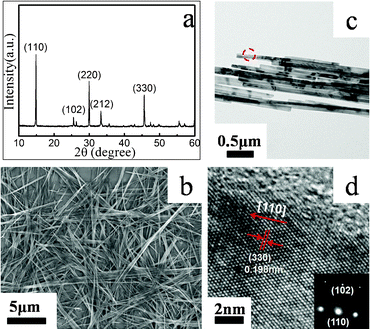 | ||
| Fig. 2 (a) XRD pattern; (b) Overview SEM image; (c) TEM image of VO2 (A) nanowires that were obtained by hydrothermal treatment at 260 °C for 8 h in the presence of 0.025 mol L−1 VOSO4, (d) High-resolution TEM image of the circular area in (c), inset is the corresponding SAED pattern. | ||
The aspect ratio of 1D VO2 (A) nanostructures can be tuned by varying the concentrations of the vanadium source. The VO2 (A) nanowires with a diameter of 70 nm and a length of over 20 μm that represents an aspect ratio of 300 were obtained by using 0.025 M of V4+ (Fig. 3a). However, doubling the V4+ concentration produced VO2 (A) nanobelts that were 100 nm in width and up to about 10 μm in length with an aspect ratio of 100 (Fig. 3b). Further increasing the vanadium source concentration to 0.1 M resulted in the formation of a large quantity of VO2 (A) nanorods that were several micrometres in length and 200–500 nm in width with an aspect ratio of 10–50 (Fig. 3c). All three nanostructures described were of a pure VO2 (A) phase and no other phase peaks or impurities were detected (Fig. 3d). The relative intensity of the (nn0) diffraction peaks in the XRD patterns of the three nanostructures were obviously stronger than others, especially for nanowires, suggesting an orientation growth along [110], which was in accord with the TEM results.
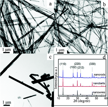 | ||
| Fig. 3 (a,b,c) TEM images and (d) XRD patterns of the products obtained by hydrothermal treatment at 260 °C for 8 h in solutions with different concentrations of VOSO4: (a) The VO2 (A) nanowires obtained in the presence of 0.025 mol L−1 VOSO4; (b) The VO2 (A) nanobelts obtained in the presence of 0.05 mol L−1 VOSO4; (c) The VO2 (A) nanorods obtained in the presence of 0.1 mol L−1 VOSO4. | ||
In order to understand the formation and growth processes of the 1D VO2 (A) nanostructures, the samples prepared at the vanadium concentration of 0.1 M were collected at different reaction times, and the corresponding time-resolved TEM and SEM images of the products are shown in Fig. 4a–g. During the initial stages (less than 2 h), the VO2 (A) mainly grows along the [110] axis by orientation attachment of VO2 (A) nanosilks to form nanowires, which can be directly observed from the TEM image (Fig. 4a) and can also be confirmed by the selected area electron diffraction (SAED). The {110} plane shows the highest surface energy and is eliminated. After growth for another 1 h, VO2 (A) nanowires begin to attach themselves to each other by a two-step process (Fig. 4b–c): contact–combination. When the reaction time is prolonged to 4 h, the VO2 (A) nanowires develop into a nanobelt, and then further grow to a nanorod through continued attachment of other nanowires and nanobelts (Fig. 4d). The inserted high resolution-TEM shows that there is a clear interface (approximately 6 nm) between nanobelts and nanowires. By further increasing the reaction time to 8 h, VO2 (A) nanobelts begin to attach and stack along the thickness orientation, resulting in the formation of VO2 (A) nanorods (Fig. 4e–f). Further increasing the reaction time only yields gradual increases in size, but no further changes in morphology occurred (Fig. 4g). These findings suggest that 1D VO2 (A) nanostructures grow through the attachment and combination model. In this formation process, the concentration of vanadium has a similar impact with reaction time. When the concentration of the vanadium source is too low, the VO2 (A) grows along [110] axis by consuming large amounts of the vanadium source. This inhibits the development of other crystal planes, thereby only forming nanowires even after a reaction time of 16 h (Figure S1, ESI†), which corresponds to the lowest energy principle.
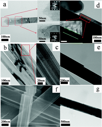 | ||
| Fig. 4 (a–g) TEM images and SEM image of the products by hydrothermal treatment in the presence of 0.1 mol L−1 VOSO4 at 260 °C for different reaction stages. (a) the reaction time is 2 h, the insets are the corresponding SAED patterns; (b–c) the reaction time is 3 h; (d) the reaction time is 4 h, the inset is the corresponding HRTEM images and the scale bar is 5 nm; (e–f) the reaction time is 8 h; (g) the reaction time is 12 h. | ||
Based on the above results, the self-assembly oriented attachment growth mechanism of 1D nanostructures VO2 (A) was schematically described in Scheme 1. The oriented attachment growth mechanism was first observed in the hydrolytic synthesis of titania by Penn and Banfield.58 This mechanism is quite distinct from Ostwald ripening, which involves the dissolution of fine particles and growth of larger particles. Nanoparticles generated in solution have a large surface-to-volume ratio, i.e. a large surface energy, which can be reduced by the oriented attachment growth and is the basis of the mechanism. Among the crystal planes of VO2 (A), {110} has the highest surface energy, and is thermodynamically favourable to be removed. At low concentrations of the vanadium precursor, the {110} crystal plane adsorbs and consumes most of the vanadium source; the nanocrystals are grown mainly along the [110] direction to form nanowires. When the concentration of vanadium source is high enough, some of the vanadium source can be consumed to make the crystal planes of low surface energies begin to grow. By prolonging the reaction time, the appearance of different orientations increases significantly. These results show that the vanadium concentration is the main requirement for morphology evolution, while the reaction time mainly influences the size of 1D VO2 (A) nanostructures. The combination of vanadium concentration and reaction time can lead to different VO2 (A) nanostructures such as nanowires, nanobelts and nanorods.
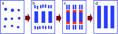 | ||
| Scheme 1 Formation mechanism of 1D VO2 (A) nanostructures. | ||
The electrochemical properties of the LIBs using the as-prepared VO2 (A) nanoparticles as cathode materials were investigated. The discharge curves and the corresponding cycle behaviour of the cell, which was cycled at a current density of 90 mA g−1 in a potential window of 1.5–4.0 V are shown in Fig. 5. The nanowire and nanobelt cathodes show a remarkably large initial discharge capacity of 277.1 mAh g−1 and 254.9 mAh g−1 (Fig. 5a), which is almost twice that of the nanorod structure (162.7 mAh g−1). Similarly, VO2 (A) nanowires exhibit the best cycling performance among three nanostructures: 116 mAh g−1 (nanowire) vs. 66.3 mAh g−1 (nanobelt) vs. 53.1 mAh g−1 (nanorod) at 50C. The VO2 (A) nanowires offer improved energy storage capacity and better cycling stabilities, namely due to their large surface areas; the BET specific surface area of nanowires is 100.22 m2 g−1, much higher than 56.95 m2 g−1 and 10.42 m2 g−1 for those of nanobelts and nanorods, respectively; a large specific area permits a high contact area with the electrolyte and short distance for lithium-ion and electron diffusion. The diffusion time varies as the square of the length, so the greater available surface area and reduction of particle sizes result in orders of magnitude increases in lithium insertion/extraction kinetics and lithium-ion flux across the electrode/electrolyte interface.
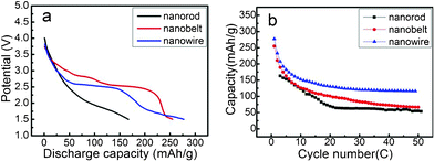 | ||
| Fig. 5 (a) First discharge profiles of as-obtained VO2 (A) nanostructures cycled between 1.5 and 4.0 V at a current density of 90 mA g−1. (b) Cycling performance of three VO2 (A) nanostructures at a rate of 90 mA g−1. | ||
However, both VO2 (A) nanowires and nanobelts exhibit a higher initial irreversible capacity loss of 16% and 17%, which are much larger than VO2 (A) nanorods (3.5%). These losses are probably due to the irreversible phase transition and the undesirable reactions with liquid electrolytes during change–recharge cycling, as reported for other vanadium oxides in the references.59,60 Actually, the formation of an intermediate layer on VO2 (A) nanowires has been experimentally observed by comparing the TEM images (Fig. 6) of VO2 (A) nanowires and nanorods before and after charge–discharge treatments. A clear amorphous film was formed on the superficial layer of the nanowires after charge–discharge treatments, but this phenomenon was not observed for the nanorods. Although the XRD patterns (Fig. 7) of VO2 (A) nanowires and nanorods after charge–discharge treatments don't reveal any impure phases, it is obvious that the nanowires are instable during charge–discharge treatments. The nanowires possessing a large surface area and small dimensions lead to increased chemical sensitivity to impurities, contaminants, and side reactions with the electrolyte. Also, the thickness of the solid electrolyte interface (SEI) layer may be larger than in the case of bulk material impeding electron and Lithium-ion transport in and out of the structure. These results serve to illustrate the importance of controlling the dimensions of nanostructure materials to optimize performance, e.g., to form an insulating layer on VO2 (A) nanowires to prohibit the contact with electrolytes.
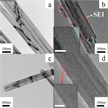 | ||
| Fig. 6 TEM images of VO2 (A) nanowires (a, b) and nanorods (c, d) before (a, c) and after (b, d) charge–discharge treatments at 90 mA g−1 for one cycle. The insets in (b) and (d) are the corresponding HRTEM images with scale bars of 5 nm. | ||
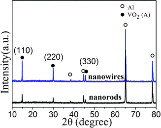 | ||
| Fig. 7 XRD patterns of VO2 (A) nanowires and nanorods after one-cycle charge–discharge treatments at 90 mA g−1. | ||
Conclusions
Different morphologies of VO2 (A) nanostructure are controllably prepared by the hydrothermal treatment of a vanadium precursor. The aspect ratios of 1D VO2 (A) nanostructures can be effectively tuned from 10 to 1000 by changing the vanadium source concentration and reaction time. When evaluated as potential cathode materials for LIBs, VO2 (A) nanowires exhibit the highest capacity (the first discharging capacity was 277.1 mAh g−1) and excellent cycling performance (the 50th discharging capacity was 116 mAh g−1), which could be ascribed to the huge surface area and short Li+ transport distance. This finding suggests that VO2 (A) is a promising new cathode material for LIBs.Acknowledgements
This study was supported in part by the One-Hundred-Talent Program of CAS, National Key Basic Research Project (NKBRP, 2009CB939904), the NSFC (50772126, 51172265, 51032008)), Shanghai Basic Research Project (09DJ1400200, 08JC1420300), the key project of CAS (4912009YC006), Shanghai Key Basic Research Program (09DJ1400200), and high-tech project of MOST (2012AA030605, 2012BAA10B03).References
- J. M. Tarascon and M. Armand, Nature, 2001, 414, 359 CrossRef CAS.
- M. Armand and J. M. Tarascon, Nature, 2008, 451, 652 CrossRef CAS.
- Y. M. Chiang, Science, 2010, 330, 1485 CrossRef CAS.
- M. S. Whittingham, Chem. Rev., 2004, 104, 4271 CrossRef CAS.
- J. B. Goodenough and Y. Kim, Chem. Mater., 2010, 22, 587 CrossRef CAS.
- L. X. Yuan, Z. H. Wang, W. X. Zhang, X. L. Hu, J. T. Chen, Y. H. Huang and J. B. Goodenough, Energy Environ. Sci., 2011, 4, 269 CAS.
- P. Balaya, Energy Environ. Sci., 2008, 1, 645 CAS.
- F. Y. Cheng, J. Liang, Z. L. Tao and J. Chen, Adv. Mater., 2011, 23, 1695 CrossRef CAS.
- C. Z. Wu and Y. Xie, Energy Environ. Sci., 2010, 3, 1191 CAS.
- H. M. Liu, Y. G. Wang, K. X. Wang, E. Hosono and H. S. Zhou, J. Mater. Chem., 2009, 19, 2835 RSC.
- T. Y. Zhai, H. M. Liu, H. Q. Li, X. S. Fang, M. Y. Liao, L. Li, H. S. Zhou, Y. Koide, Y. Bando and D. Goberg, Adv. Mater., 2010, 22, 2547 CrossRef CAS.
- J. Liu, H. Xia, D. F. Xue and L. Lu, J. Am. Chem. Soc., 2009, 131, 12086 CrossRef CAS.
- Y. S. Hu, X. Liu, J. O. Muller, R. Schlogl, J. Maier and D. S. Su, Angew. Chem., Int. Ed., 2009, 48, 210 CrossRef CAS.
- Y. Wang and G. Z. Cao, Adv. Mater., 2008, 20, 2251 CrossRef CAS.
- A. M. Cao, J. S. Hu, H. P. Liang and L. J. Wan, Angew. Chem., Int. Ed., 2005, 44, 4391 CrossRef CAS.
- C. G. Chen, Y. P. Liu and L. Li, J. Inorg. Mater., 2004, 19, 1225 CAS.
- T. Schmitt, A. Augustsson, L. C. Duda, J. Nordgren, J. Howing and T. Gustafsson, J. Appl. Phys., 2004, 95, 6444 CrossRef CAS.
- M. S. Whittingham, Science, 1976, 192, 1126 CAS.
- A. Q. Pan, J. G. Zhang, Z. M. Nie, G. Z. Cao, B. W. Arey, G. S. Li, S. Q. Liang and J. Liu, J. Mater. Chem., 2010, 20, 9193 RSC.
- T. Watanabe, Y. Ikeda, T. Ono, M. Hibino, M. Hosoda, K. Sakai and T. Kudo, Solid State Ionics, 2002, 151, 313 CrossRef CAS.
- J. Muster, G. T. Kim, V. Krstic, J. G. Park, Y. W. Park, S. Roth and M. Burghard, Adv. Mater., 2000, 12, 420 CrossRef CAS.
- Y. Z. Li, T. Kunitake and Y. Aoki, Chem. Mater., 2007, 19, 575 CrossRef CAS.
- C. Leroux, G. Nihoul and G. Van Tendeloo, Phys. Rev. B: Condens. Matter, 1998, 57, 5111 CrossRef CAS.
- F. J. Morin, Phys. Rev. Lett., 1959, 3, 34 CrossRef CAS.
- L. T. Kang, Y. F. Gao and H. J. Luo, ACS Appl. Mater. Interfaces, 2009, 1, 2211 CAS.
- Z. T. Zhang, Y. F. Gao, Z. Chen, J. Du, C. X. Cao, L. T. Kang and H. J. Luo, Langmuir, 2010, 26, 10738 CrossRef CAS.
- C. X. Cao, Y. F. Gao and H. J. Luo, J. Phys. Chem. C, 2008, 112, 18810 CAS.
- L. Dai, C. X. Cao, Y. F. Gao and H. J. Luo, Sol. Energy Mater. Sol. Cells, 2011, 95, 712 CrossRef CAS.
- S. D. Zhang, Y. M. Li, C. Z. Wu, F. Zheng and Y. Xie, J. Phys. Chem. C, 2009, 113, 15058 CAS.
- Y. Oka, T. Yao and N. Yamamoto, J. Solid State Chem., 1990, 86, 116 CrossRef CAS.
- J. Galy, J. Solid State Chem., 1999, 148, 224 CrossRef CAS.
- A. M. Kannan and A. Manthiram, Solid State Ionics, 2003, 159, 265 CrossRef CAS.
- G. Armstrong, J. Canales, A. R. Armstrong and P. G. Bruce, J. Power Sources, 2008, 178, 723 CrossRef CAS.
- C. V. S. Reddy, E. H. Walker, S. A. Wicker, Q. L. Williams and R. R. Kalluru, Curr. Appl. Phys., 2009, 9, 1195 CrossRef.
- Z. J. Chen, S. K. Gao, L. L. Jiang, M. D. Wei and K. M. Wei, Mater. Chem. Phys., 2010, 121, 254 CrossRef CAS.
- F. Wang, Y. Liu and C. Y. Liu, Electrochim. Acta, 2010, 55, 2662 CrossRef CAS.
- J. A. Ni, W. T. Jiang, K. Yu, Y. F. Gao and Z. Q. Zhu, Electrochim. Acta, 2011, 56, 2122 CrossRef CAS.
- F. Theobald, J. Less Common Met., 1977, 53, 55 CrossRef CAS.
- T. Yao, Y. Oka and N. Yamamoto, J. Solid State Chem., 1994, 112, 196 CrossRef CAS.
- Y. Oka, S. Sato, T. Yao and N. Yamamoto, J. Solid State Chem., 1998, 141, 594 CrossRef CAS.
- S. D. Ji, Y. G. Zhao, F. Zhang and P. Jin, J. Ceram. Soc. Jpn., 2010, 118, 867 CrossRef CAS.
- P. Poizot, S. Laruelle, S. Grugeon, L. Dupont and J. M. Tarascon, Nature, 2000, 407, 496 CrossRef CAS.
- A. S. Arico, P. Bruce, B. Scrosati, J. M. Tarascon and W. Van Schalkwijk, Nat. Mater., 2005, 4, 366 CrossRef CAS.
- P. G. Bruce, B. Scrosati and J. M. Tarascon, Angew. Chem., Int. Ed., 2008, 47, 2930 CrossRef CAS.
- B. Kang and G. Ceder, Nature, 2009, 458, 190 CrossRef CAS.
- Y. K. Sun, S. T. Myung, B. C. Park, J. Prakash, I. Belharouak and K. Amine, Nat. Mater., 2009, 8, 320 CrossRef CAS.
- S. Wang, S. Li, Y. Sun, X. Feng and C. Chen, Energy Environ. Sci., 2011, 4, 2854 CAS.
- Y. Wang, K. Takahashi, K. Lee and G. Z. Cao, Adv. Funct. Mater., 2006, 16, 1133 CrossRef CAS.
- L. Q. Mai, L. Xu, C. H. Han, Y. Z. Luo, S. Y. Zhao and Y. L. Zhao, Nano Lett., 2010, 10, 4750 CrossRef CAS.
- H. W. Lee, P. Muralidharan, R. Ruffo, C. M. Mari, Y. Cui and D. K. Kim, Nano Lett., 2010, 10, 3852 CrossRef CAS.
- P. Meduri, C. Pendyala, V. Kumar, G. U. Sumanasekera and M. K. Sunkara, Nano Lett., 2009, 9, 612 CrossRef CAS.
- H. M. Liu, Y. G. Wang, K. X. Wang, Y. R. Wang and H. S. Zhou, J. Power Sources, 2009, 192, 668 CrossRef CAS.
- L. F. Cui, Y. Yang, C. M. Hsu and Y. Cui, Nano Lett., 2009, 9, 3370 CrossRef CAS.
- L. F. Cui, R. Ruffo, C. K. Chan, H. L. Peng and Y. Cui, Nano Lett., 2009, 9, 491 CrossRef CAS.
- C. K. Chan, X. F. Zhang and Y. Cui, Nano Lett., 2008, 8, 307 CrossRef CAS.
- M. S. Park, G. X. Wang, Y. M. Kang, D. Wexler, S. X. Dou and H. K. Liu, Angew. Chem., Int. Ed., 2007, 46, 750 CrossRef CAS.
- L. Q. Mai, X. Xu, L. Xu, C. H. Han and Y. Z. Luo, J. Mater. Res., 2011, 26, 2175 CrossRef CAS.
- R. L. Penn and J. F. Banfield, Geochim. Cosmochim. Acta, 1999, 63, 1549 CrossRef CAS.
- D. W. Murphy, P. A. Christian, F. J. Disalvo and J. N. Carides, J. Electrochem. Soc., 1979, 126, 497 CrossRef CAS.
- S. H. Lee, H. M. Cheong, P. Liu and C. E. Tracy, Electrochem. Solid-State Lett., 2003, 6, A102 CrossRef CAS.
Footnote |
| † Electronic supplementary information (ESI) available. See DOI: 10.1039/c2ra20587d |
| This journal is © The Royal Society of Chemistry 2012 |