Interfacial modification of photoelectrode in ZnO-based dye-sensitized solar cells and its efficiency improvement mechanism
Jie
Guan
a,
Jiyuan
Zhang
a,
Tao
Yu
*a,
Guogang
Xue
a,
Xirui
Yu
a,
Zekun
Tang
a,
Yulong
Wei
a,
Jie
Yang
a,
Zhaosheng
Li
b and
Zhigang
Zou
ab
aNational Laboratory of Solid State Microstructures, Eco-materials and Renewable Energy Research Center (ERERC), Department of Physics, Nanjing University, Nanjing 210093, P. R. China. E-mail: yutao@nju.edu.cn
bDepartment of Materials Science and Engineering, Nanjing University, Nanjing 210093, P. R. China
First published on 25th June 2012
Abstract
A ZnO compact layer prepared by a sol–gel method was introduced into a photoelectrode at the interface between fluorine-doped tin oxide (FTO) substrate and a mesoporous ZnO layer in ZnO-based dye-sensitized solar cells (DSSCs). The ZnO compact layer was characterized by field-emission scanning electron microscopy (FE-SEM), atomic force microscopy (AFM) and UV-Vis spectroscopy. The compact layer increased the photoelectric conversion efficiency of ZnO-based DSSCs by 20%. An electrochemical impedance spectroscopy (EIS) study demonstrated that the compact layer strikingly reduced the interfacial resistance in the device by enhancing the conductive contact between nanocrystalline ZnO and FTO substrate. The photocurrent density–voltage characteristics in the dark suggests that the compact ZnO layer also plays the role of a blocking layer suppressing the charge recombination, which is illustrated by the suppression of dark current density. The two effects effectively elevate the short circuit current density (JSC) and open circuit voltage (VOC), and finally improve the overall conversion efficiency of ZnO-based DSSCs.
1. Introduction
Dye-sensitized solar cells (DSSCs) based on dye-sensitized wide-band-gap nanocrystalline semiconductors have offered a promising alternative to conventional photovoltaic devices due to their low cost and simple fabrication processes. The highest efficiency of DSSCs based on TiO2 has now reached 12%.1–4 Typical DSSCs consist of transparent conducting oxide (TCO) substrates, dye-sensitized mesoporous TiO2 photoelectrodes with high specific surface area, liquid redox electrolyte and Pt counter electrodes. Many factors affect the efficiency improvement of DSSCs, such as the ability of the dye to harvest sunlight,5–9 the capacity of electron transport and collection of the nanostructure semiconductor photoelectrode.10–14 There are many interfaces in nanocrystalline semiconductor/TCO/electrolyte/counter electrode photoelectrochemical systems and interfacial modification can be expected to improve the efficiency of DSSCs. It has been reported that a compact blocking layer between TCO and nanocrystalline TiO2 layer can enhance the performance of TiO2-based DSSCs, benefiting from both the reduced interfacial resistance and the TCO/redox electrolyte direct contact.15–23ZnO is another attractive wide-band-gap semiconductor, which possesses a similar energy band structure to TiO2 (Eg = 3.2 eV) but has higher electron mobility (102 cm2 V−1 s−1) and richer nano/micro structures than that of TiO2. A number of studies have already been reported on the use of ZnO for application in DSSCs.14,24–36 Although so far the results obtained for ZnO-based DSSCs have shown relatively lower overall conversion efficiencies than those of TiO2, ZnO is still regarded as a promising alternative to TiO2 due to its ease of crystallization and anisotropic growth. The limited performance in ZnO-based DSSCs has been believed basically to result from the instability of ZnO in acidic dye and the slow electron-injection kinetics from the dye to ZnO.24,25 Several methods have been attempted to solve these problems and improve the efficiency. Law et al. have fabricated ZnO–Al2O3 and ZnO–TiO2 core–shell nanowire photoelectrodes to suppress recombination in DSSCs.30 Matsui et al. have synthesized new type of photosensitizers for ZnO-based DSSCs.31 In addition, functional nanostructured ZnO photoelectrodes have been extensively studied for efficiency improvement of DSSCs, such as nanowires,32 nanotubes,33 nanotrees,34 nanosheets14,35 and nanotips.36 Considering the charge transportation in crystalline ZnO benefits from high electron mobility, it is quite possible that the interface between ZnO and TCO becomes the bottleneck of charge transportation in DSSCs. Efficiency improvement of ZnO-based DSSCs might be achieved by modifying the interface between ZnO/TCO, just as has been done in TiO2-based DSSCs.15–23 The introduction of a compact layer between the ZnO/TCO interface has already been demonstrated to be effective in ZnO-based DSSCs.37–39 However, the mechanism for the effect of the compact layer to ZnO-based DSSCs was seldom studied. Perez-Hernandez et al. discussed the effect of the compact interlayer prepared by rf magnetron sputtering on the performance of ZnO-based DSSCs, but they did not improve the efficiency markedly,40 which might be due to the unsuitability of the preparation method for the interlayer.
In this work, a compact layer of ZnO prepared conveniently was introduced at the interface between nanocrystalline ZnO and fluorine-doped tin oxide (FTO) substrate in DSSCs, which improved the efficiency of ZnO-based DSSCs. In addition, the mechanism of the influence to the efficiency of the ZnO compact layer was discussed. The main effect of the compact layer is shown in Fig. 1, in which the yellow arrows represent the collected current and the red ones represent the recombination current. Electrochemical impedance spectroscopy (EIS) study suggests that this layer strikingly reduces the interfacial resistance by enhancing the contact with FTO, and the compact ZnO layer also plays the role of a blocking layer suppressing the charge recombination, which is confirmed by the suppression of dark current density.
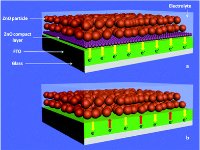 | ||
| Fig. 1 Schematic diagram of ZnO nanocrystalline photoelectrode with (a) and without (b) compact layer. | ||
2. Experimental
The ZnO compact layer was prepared by a sol–gel method that had been reported previously.41 In short, after zinc acetate was first dissolved in anhydrous ethanol at 80 °C, diethanolamine (DEA) was added into the solution as the sol stabilizer under stirring and then kept stirring for 30 min till a transparent sol was obtained. The molar ratio of DEA to zinc acetate was set at 1.0. Zinc acetate sols at various concentrations (0.05–0.5 M) of Zn were coated on clean FTO substrates by a spin-coater for 10 s with a spinning speed of 2000 rpm. After being dried, the coated films were sintered at 500 °C for an hour to form ZnO compact layers.The surface morphologies of the ZnO/FTO substrates were examined by field emission scanning electron microscopy (FE-SEM, FEI NOVA NANOSEM 230) and atomic force microscopy (AFM, JPK NANOWIZARD II). Absorption spectra were measured on a Shimadzu UV-2550 UV-Vis spectrometer fitted with an integrating sphere.
Sodium carbonate and zinc acetate solution (each 0.5 M) were mixed under vigorous stirring for 1 h and the obtained suspension was triply centrifuged, washed with ethanol and then dried at 60 °C to form ZnO nanoparticles. To fabricate the photoelectrodes for DSSCs, nanocrystalline ZnO films were prepared on both bare FTO and FTO/ZnO substrates according to the procedure described as reported.42 To characterize the photoelectric performance, the ZnO electrode was sensitized by soaking it in 0.5 mM bis(tetrabutylammonium) cis-bis(thiocyanato)bis(2,2′-bipyridine-4-carboxylic acid-4′-carboxylate)ruthenium(II) dye solution (N719 Solaronix S A, Switzerland) in ethanol (HPLC grade, Fisher) solution for 2 h.
Current–voltage (I–V) measurements and the amount of adsorbed dye measurements were described in previous work of our group.14 Impedance spectrum measurements were performed with a PARSTAT 2273 advanced electrochemical system (Princeton Applied Research, USA) under illumination. The frequency range was 0.02–100 kHz and the magnitude of modulation signal was 10 mV.
3. Results and discussion
3.1. Characterization of the ZnO compact layer on FTO substrate
Fig. 2 presents FE-SEM images and three-dimensional AFM height morphologies of the surfaces of ZnO compact layers on the FTO substrates obtained from zinc acetate solutions of different concentrations. It can be seen that the tiny ZnO nanoparticles connect with each other and form a compact layer on the FTO substrate. As the concentration of the zinc acetate solution is increased, the size of the ZnO particles becomes bigger. Particularly, when the concentration of zinc acetate solutions is 0.2 or 0.5 M, the layer surfaces become quite rough with more interstices between ZnO particles and so the ZnO layer is less compact.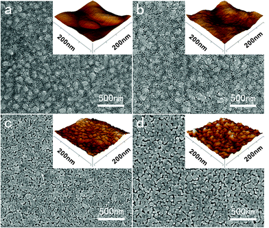 | ||
| Fig. 2 FE-SEM images and three-dimensional AFM height morphologies (insets) of FTO and ZnO compact layers prepared from zinc acetate solutions (a) 0.05 M, (b) 0.1 M, (c) 0.2 M, (d) 0.5 M after sintering at 500 °C. | ||
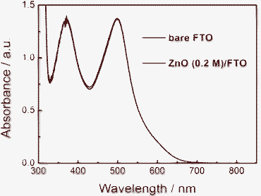
Optical properties of the ZnO/FTO substrates were investigated since light was utilised by the DSSCs after transmitting through the substrates. Fig. 3 shows the UV-Vis absorption spectra of bare FTO and compact ZnO coated FTO substrates. The absorption of FTO substrates coated with ZnO films showed little change compared with bare FTO in the region from 400 to 800 nm. However, as the concentration of zinc acetate was increased, the absorption of the ZnO/FTO substrate increased gradually in the region from 300 to 400 nm. For the whole range of sunlight, the ZnO films (especially when the zinc acetate concentration is less than 0.2 M) scarcely did not influence the light harvesting of DSSCs. The absorptions of ZnO/FTO substrates with zinc acetate concentration of 0.2 and 0.5 M are raised clearly in the region from 350 to 400 nm, which will slightly affect the light harvesting efficiency of the devices. The band gap of ZnO is 3.2 eV and the corresponding wavelength of the absorption edge is about 380 nm, so the ZnO compact layer mainly affects the absorption in the region from 350 to 400 nm. Besides, as the zinc acetate concentration rises, the thickness of the ZnO layer increases. As a result, the absorption of ZnO/FTO substrates with high zinc acetate concentration is raised between 350 and 400 nm.
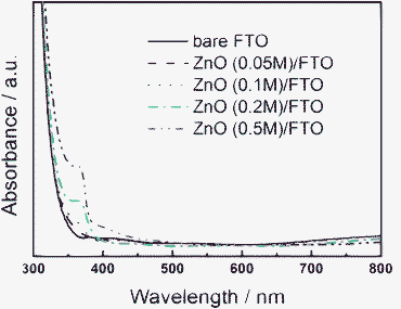 | ||
| Fig. 3 Optical absorption spectra of bare FTO and ZnO/FTO substrates with different concentrations of zinc acetate. | ||
3.2. Effect of ZnO compact layer on photoelectric performance
Current density–voltage (J–V) curves of DSSCs based on FTO and ZnO/FTO substrates under AM1.5 (100 mW cm−2) illumination with an active area of 0.132 cm2 are presented in Fig. 4. The parameters of the J–V curves are listed in Table 1, including open circuit voltage (VOC), short circuit current density (JSC), fill factor (FF) and efficiency (η). All the samples have the same film thickness of about 15 μm. Without the compact layer, the VOC, JSC, FF of the device are 0.536 V, 7.55 mA cm−2, 0.681, respectively, and the final efficiency is 2.76%. After a ZnO compact layer was spin-coated at the interface between nanocrystalline ZnO and FTO substrate, the efficiency of the device is improved when the concentration of zinc acetate is 0.05 and 0.1 M, due to the elevation of JSC and VOC. Especially in the case that the concentration of zinc acetate is 0.1 M, the device gives the highest energy conversion efficiency of 3.34%, which is improved by 20% compared to that without a compact layer. However, when the concentration of zinc acetate is more than 0.1 M, JSC decreases and this results in the reduction of energy conversion efficiency. This is because as the concentration of zinc acetate is increased, the ZnO layer becomes thicker and shows a higher absorption of light, as shown in Fig. 3. Thus part of the light used by the device is lost and then JSC decreases. Fig. 5 shows the monochromatic incident photon-to-electron conversion efficiency (IPCE) of DSSCs based on bare FTO and ZnO/FTO substrates with different concentrations of zinc acetate. The peak value of IPCE of the sample without a compact layer is about 42%. After the compact layer is introduced, the peak value of IPCE is increased to about 50% with 0.1 M zinc acetate concentration while it is decreased to about 37% with 0.5 M zinc acetate concentration. The results are in accord with those of the J–V curves.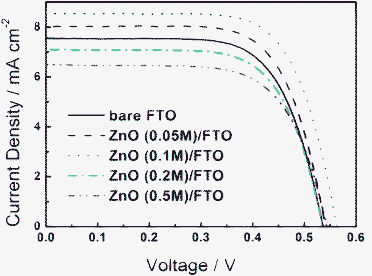 | ||
| Fig. 4 Current density–voltage characteristics of DSSCs based on bare FTO and ZnO/FTO substrates with different concentrations of zinc acetate under AM 1.5 illumination. | ||
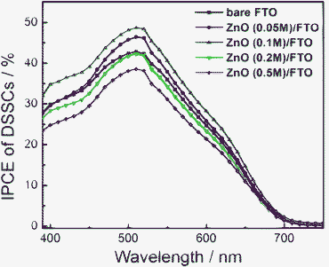 | ||
| Fig. 5 IPCE of DSSCs based on bare FTO and ZnO/FTO substrates with different concentrations of zinc acetate. | ||
| Sample | V OC/V | J SC/mA cm−2 | FF (%) | η (%) |
|---|---|---|---|---|
| Bare FTO | 0.536 | 7.55 | 68.13 | 2.76 |
| ZnO (0.05 M)/FTO | 0.541 | 8.03 | 69.17 | 3.00 |
| ZnO (0.1 M)/FTO | 0.563 | 8.55 | 69.53 | 3.34 |
| ZnO (0.2 M)/FTO | 0.535 | 7.10 | 68.17 | 2.59 |
| ZnO (0.5 M)/FTO | 0.544 | 6.49 | 67.47 | 2.38 |
In DSSCs, JSC is determined by the light harvesting efficiency, charge injection efficiency and charge collection efficiency. In addition, it is rational to assume the same injection efficiency for the given ZnO/N719 systems. Thus the improvement of JSC originates from an improvement in light harvesting efficiency and/or charge collection efficiency, which are affected by the dye amount adsorbed on the photoelectrode and charge transport. To investigate the origin of the improvement of energy conversion efficiency, the adsorbed dye of nanocrystalline ZnO films with the same film area and thickness on substrates without compact layer and with compact layer obtained from 0.1 M zinc acetate was desorbed by NaOH aqueous solution. Fig. 6 shows the absorption spectra of the two solutions. As is shown in the figure the two curves nearly overlapped. This indicates that the electrodes on the two substrates adsorbed almost the same amount of dye and so have similar light harvesting capabilities. Thus the enhancement in JSC is mainly ascribed to the improvement of the electron collection.
 | ||
| Fig. 6 Optical absorption spectra of N719 desorbed from ZnO photoelectrodes based on bare FTO and ZnO/FTO substrates with 0.1 M zinc acetate concentration. | ||
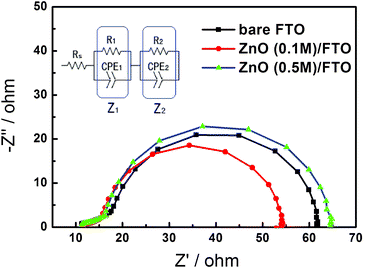
To further investigate the origin of improvement of energy conversion efficiency, electrochemical impedance spectroscopy was conducted. EIS is regarded as the most effective technique to investigate charge transport phenomena in DSSCs. Fig. 7 shows Nyquist plots of DSSCs based on bare FTO, ZnO (0.1 M)/FTO and ZnO (0.5 M)/FTO substrates by EIS analysis under illumination. The resistance component (RS) in the high-frequency region (>106 Hz) is related to the sheet resistance of the TCO layer. The other impedance components observed in the frequency regions of 103–105 (ω1), 1–103 (ω2) and 0.1–1 (ω3) Hz are associated with the charge transport at the TCO/photoelectrode and Pt counter electrode/electrolyte interfaces (Z1), the photoelectrode/dye/electrolyte interfaces (Z2), and the Nernstian diffusion in the electrolyte (Z3), respectively.43,44 In DSSCs, the component at low frequencies (Z3) usually does not appear in actual EIS measurements. Table 2 summarizes the results of the EIS analysis fitted by using an equivalent circuit shown in the inset of Fig. 7. It can be seen that RS remains constant (10.50 + 0.40 Ω), regardless of the compact layer, as identical FTO substrates are employed for all the samples. The resistance of the Z1 component (R1), which is given by the sum of resistances of counter electrode/electrolyte and FTO/ZnO interfaces here, decreases significantly as a function of the additional compact layer. Since the Pt counter electrode/electrolyte interface is the same for each device, the difference in the FTO/ZnO interface is wholly responsible for the difference in R1. The value of R1 of the cell sample based on ZnO (0.1 M)/FTO (6.77 Ω) and ZnO (0.5 M)/FTO (9.04 Ω) substrates is lower than that of bare FTO substrate (11.57 Ω). This result illustrates that the compact layer decreases the interfacial resistance between ZnO and FTO. Especially when the concentration of zinc acetate is 0.1 M, the obtained ZnO layer makes the best contact of FTO and nanocrystalline ZnO electrode, and so leads to the lowest interfacial resistance. The value of R2, the resistance of interfacial charge transfer from the dye-sensitized ZnO photoelectrode to triiodide in the electrolyte, based on ZnO (0.1 M)/FTO substrate (36.59 Ω) decreases compared to that based on bare FTO substrate (40.79 Ω). This is due to the whole essential resistance decreasing because of the compact layer and then the photocurrent density increased. As a result, electron density in the conductive band of ZnO increases when the device is at work and causes the decrease of R2. Similarly, as mentioned before, the sample based on ZnO (0.5 M) substrate has relatively poorer light harvesting and has lower photocurrent density. Therefore, R2 of the sample based on ZnO (0.5 M) substrate (45.68 Ω) is increased compared to that based on bare FTO substrate due to the decrease of electron density in ZnO. The EIS data we obtained is also in complete accord with the results of analogous works in TiO2-based DSSCs, which have been reported previously.18,22
 | ||
| Fig. 7 Nyquist plots of DSSCs based on bare FTO, ZnO (0.1 M)/FTO and ZnO (0.5 M)/FTO substrates under illumination. The inset shows the equivalent circuit. | ||
| Sample | R S/Ω | R 1/Ω | R 2/Ω |
|---|---|---|---|
| Bare FTO | 10.13 | 11.57 | 40.79 |
| ZnO (0.1 M)/FTO | 10.84 | 6.77 | 36.59 |
| ZnO (0.5 M)/FTO | 10.16 | 9.04 | 45.68 |
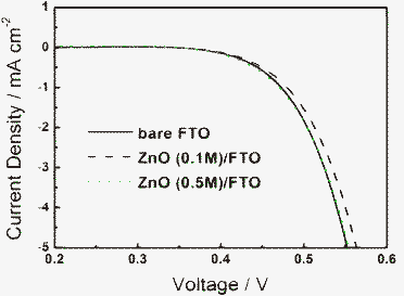
To investigate the influence of the compact layer to charge recombination in DSSCs, the current density–voltage characteristics were also measured in the dark. As shown in Fig. 8, the onset of the dark current of the sample based on ZnO (0.1 M)/FTO is shifted markedly to more positive voltage compared to bare FTO and ZnO (0.5 M)/FTO. This demonstrates that the ZnO layer obtained by spin-coating 0.1 M zinc acetate solution successfully suppresses back electron transfer from FTO to the electrolyte. When the concentration of zinc acetate is 0.5 M, the obtained ZnO layer is assembled by relatively bigger ZnO nanoparticles and was less compact, which can be seen in the SEM images, and so the obtained ZnO layer has little effect as a compact blocking layer in the ZnO-based DSSCs.
 | ||
| Fig. 8 Dark current characteristics of DSSCs based on bare FTO, ZnO (0.1 M)/FTO and ZnO (0.5 M)/FTO substrates. | ||
4. Conclusions
In conclusion, we introduced a compact layer of ZnO at the interface between nanocrystalline ZnO and FTO substrate in ZnO-based DSSCs by a spin-coating method. The compact layer enhanced the contact of the interface between ZnO photoelectrode and FTO and strikingly reduced the interfacial resistance, which was confirmed by EIS analysis. Moreover, the compact layer suppressed the dark current density compared to the DSSCs based on bare FTO substrate, indicating the blocking layer effect of the ZnO compact layer. Finally, the JSC and VOC were improved markedly and the photovoltaic energy conversion efficiency reached 3.34% when the concentration of zinc acetate was 0.1 M, which was enhanced by 20% compared to bare FTO-based DSSCs.Acknowledgements
We thank the financial support from the National Natural Science Foundation of China (Grant Nos. 11174129, 50902068 and 51102132), the National Basic Research Program of China (Grants No. 2011CB933303), the Jiangsu Provincial Science and Technology Research Program (Grant No. BK2011056). The work is supported by the Fundamental Research Funds for the Central Universities (Grant No. 1116020406). We thank the AFM experimental help from Professor Yi Cao and Mr. Xiaotian Han. The invaluable discussions from Professor Jianguo Liu in revising the manuscript are also gratefully acknowledged.References
- B. O'Regan and M. Gratzel, Nature, 1991, 353, 737 CrossRef CAS.
- M. K. Nazeeruddin, F. D. Angelis, S. Fantacci, A. Selloni, G. Viscardi, P. Liska, S. Ito, B. Takeru and M. Gratzel, J. Am. Chem. Soc., 2005, 127, 16835 CrossRef CAS.
- M. Gratzel, Acc. Chem. Res., 2009, 42, 1788 CrossRef CAS.
- A. Hagfeldt, G. Boschloo, L. Sun, L. Kloo and H. Pettersson, Chem. Rev., 2010, 110, 6595 CrossRef CAS.
- M. K. Nazeeruddin, P. Pechy, T. Renouard, S. M. Zakeeruddin, R. Humphry-Baker, P. Liska, L. Cevey, E. Coata, V. Shklover, L. Spiccia, G. B. Deacon, C. A. Bignozzi and M. Gratzel, J. Am. Chem. Soc., 2001, 123, 1613 CrossRef CAS.
- Z. Yu, H. M. Najafabadi, Y. Xu, K. Nonomura, L. Sun and L. Kloo, Dalton Trans., 2011, 40, 8361 RSC.
- D. H. Lee, M. J. Lee, H. M. Song, B. J. Song, K. D. Seo, M. Pastore, C. Anselmi, S. Fantacci, F. D. Angelis, M. K. Nazeeruddin, M. Graetzel and H. K. Kim, Dyes Pigm., 2011, 91, 192 CrossRef CAS.
- O. A. Blackburn, B. J. Coe, V. Hahn, M. Helliwell, J. Raftery, Y. T. Ta, L. M. Peter, H. Wang, J. A. Anta and E. Guillen, Dyes Pigm., 2012, 92, 766 CrossRef CAS.
- W. Zhou, B. Zhao, P. Shen, S. Jiang and H. Huang, Dyes Pigm., 2011, 91, 404 CrossRef CAS.
- K. Zhu, N. R. Neale, A. Miedaner and A. J. Frank, Nano Lett., 2007, 7, 69 CrossRef CAS.
- R. Zhang, S. Kumar, S. Z. Zou and L. L. Kerr, Cryst. Growth Des., 2008, 8, 381 CAS.
- F. Hao, H. Lin, C. Zhou, Y. Z. Liu and J. B. Li, Phys. Chem. Chem. Phys., 2011, 13, 15918 RSC.
- S. Huang, X. Z. Guo, X. M. Huang, Q. X. Zhang, H. C. Sun, D. M. Li, Y. H. Luo and Q. B. Meng, Nanotechnology, 2011, 22, 315402 CrossRef.
- X. Y. Wang, Z. P. Tian, T. Yu, H. M. Tian, J. Y. Zhang, S. K. Yuan, X. B. Zhang, Z. S. Li and Z. G. Zou, Nanotechnology, 2010, 21, 065703 CrossRef.
- J. Kim, J. Kim and M. Lee, Nanotechnology, 2010, 21, 345203 CrossRef.
- L. Chen, C. Chen and B. Tseng, J. Nanomater., 2010, 374052 Search PubMed.
- J. B. Xia, N. Masaki, K. J. Jiang and S. Yanagida, J. Phys. Chem. B, 2006, 110, 25222 CrossRef CAS.
- S. Lee, J. H. Noh, H. S. Han, D. K. Yim, D. H. Kim, J. Lee, J. Y. Kim, H. S. Jung and K. S. Hong, J. Phys. C, 2009, 113, 6878 CAS.
- S. Roh, R. S. Mane, S. Min, W. Lee, C. D. Lokhande and S. Han, Appl. Phys. Lett., 2006, 89, 253512 CrossRef.
- Y. M. Liu, X. M. Sun, Q. D. Tai, H. Hu, B. L. Chen and N. Huang, J. Power Sources, 2011, 196, 475 CrossRef CAS.
- H. Yu, S. Q. Zhang, H. J. Zhao, G. Will and P. Liu, Electrochim. Acta, 2009, 54, 1319 CrossRef CAS.
- Y. J. Kim, Y. H. Lee, M. H. Lee, H. J. Kim, J. H. Pan, G. I. Lim, Y. S. Choi, K. Kim, N. Park, C. Lee and W. I. Lee, Langmuir, 2008, 24, 13225 CrossRef CAS.
- K. S. Ahn, M. S. Kang, J. W. Lee and Y. S. Kang, J. Appl. Phys., 2007, 101, 084312 CrossRef.
- Q. Zhang, C. S. Dandeneau, X. Zhou and G. Cao, Adv. Mater., 2009, 21, 4087 CrossRef CAS.
- M. Quintana, T. Edvinsson, A. Hagfeldt and G. Boschloo, J. Phys. Chem. C, 2007, 111, 1035 CAS.
- Z. G. Chen, Y. W. Tang, L. S. Zhang and L. J. Luo, Electrochim. Acta, 2006, 51, 5870 CrossRef CAS.
- K. Keis, E. Magnusson, H. Lindstrom, S. Lindquist and A. Hagfeldt, Sol. Energy Mater. Sol. Cells, 2002, 73, 51 CrossRef.
- M. Matsui, M. Kotani, Y. Kubota, K. Funabiki, J. Jin, T. Yoshida, S. Higashijima and H. HMiura, Dyes Pigm., 2011, 91, 145 CrossRef CAS.
- L. Luo, W. Tao, X. Hu, T. Xiao, B. Heng, W. Huang, H. Wang, H. Han, Q. Jiang, J. Wang and Y. Tang, J. Power Sources, 2011, 196, 10518 CrossRef CAS.
- M. Law, L. E. Greene, A. Radenovic, T. Kuykendall, J. Liphardt and P. D. Yang, J. Phys. Chem. A, 2006, 110, 22652 CrossRef CAS.
- M. Matsui, Y. Hashimoto, K. Funabiki, J. Y. Jin, T. Yoshida and H. Minoura, Synth. Met., 2005, 148, 147 CrossRef CAS.
- M. Law, L. E. Greene, J. C. Johnson, R. Saykally and P. D. Yang, Nat. Mater., 2005, 4, 455 CrossRef CAS.
- A. B. Martinson, J. W. Elam, J. T. Hupp and M. J. Pellin, Nano Lett., 2007, 7, 2183 CrossRef CAS.
- S. H. Ko, D. Lee, H. W. Kang, K. H. Nam, J. Y. Yeo, S. J. Hong, C. P. Grigoropoulos and H. J. Sung, Nano Lett., 2011, 11, 666 CrossRef CAS.
- C. Y. Lin, Y. H. Lai, H. W. Chen, J. G. Chen, C. W. Kung, R. Vittal and K. C. Ho, Energy Environ. Sci., 2011, 4, 3448 CAS.
- H. Chen, A. D. Pasquier, G. Saraf, J. Zhong and Y. Lu, Semicond. Sci. Technol., 2008, 23, 045004 CrossRef.
- Z. G. Chen, Y. W. Tang, L. S. Zhang and L. J. Luo, Electrochim. Acta, 2006, 51, 5870 CrossRef CAS.
- Y. Z. Zhang, L. H. Wu, Y. P. Liu and E. Q. Xie, J. Phys. D: Appl. Phys., 2009, 42, 085105 CrossRef.
- Y. Q. Wang, Y. M. Sun and K. Li, Mater. Lett., 2009, 63, 1102 CrossRef CAS.
- G. Perez-Hernandez, A. Vega-Poot, I. Perez-Juarez, J. M. Camacho, O. Ares, V. Rejon, J. L. Pena and G. Oskam, Sol. Energy Mater. Sol. Cells, 2012, 100, 21 CrossRef CAS.
- Y. D. Zhang, W. J. Fa, F. L. Yang, A. Zheng and P. Y. Zhang, Ionics, 2010, 16, 815 CrossRef CAS.
- S. Ito, P. Chen, P. Comte, M. K. Nazeeruddin, P. Liska, P. Pechy and M. Gratzel, Progr. Photovolt.: Res. Appl., 2007, 15, 603 CrossRef CAS.
- R. Kern, R. Sastrawan, J. Ferber, R. Stangl and J. Luther, Electrochim. Acta, 2002, 47, 4213 CrossRef CAS.
- L. Y. Han, N. Koide, Y. Chiba and T. Mitate, Appl. Phys. Lett., 2004, 84, 2433 CrossRef CAS.
| This journal is © The Royal Society of Chemistry 2012 |