Enhanced conversion efficiency of flexible dye-sensitized solar cells by optimization of the nanoparticle size with an electrophoretic deposition technique†
Zhaosheng
Xue
ab,
Wei
Zhang
a,
Xiong
Yin
ac,
Yueming
Cheng
a,
Long
Wang
a and
Bin
Liu
*ad
aDepartment of Chemical and Biomolecular Engineering, National University of Singapore, Singapore 117576. E-mail: cheliub@nus.edu.sg
bNUS Graduate School for Integrative Sciences & Engineering (NGS), National University of Singapore, Singapore 117456
cNational Center for Nanoscience and Technology, P. R. China
dInstitute of Materials Research and Engineering, 3 Research Link, Singapore 117602
First published on 28th May 2012
Abstract
To optimize the conversion efficiency of plastic dye-sensitized solar cells fabricated by the electrophoretic deposition technique, anatase TiO2 nanoparticles of various sizes from 10 nm to 27 nm have been synthesized via a simple hydrothermal process. The obtained TiO2 nanoparticles have been characterized by X-ray diffraction and high resolution transmission electron microscopy, which confirmed that the synthesized nanoparticles are in the pure anatase phase. Rigid devices based on D149-sensitized TiO2 particles with a size of 19 nm showed the highest conversion efficiency of 7.0% among the four different devices, which was measured under illumination of AM 1.5G, 100 mWcm−2. The effect of the particle size on the photovoltaic performance of DSSCs has been systemically studied using photoelectrochemical characterizations, including intensity modulated photocurrent spectroscopy and intensity modulated photovoltage spectroscopy. The good photovoltaic performance for 19 nm TiO2 is ascribed to the good dye loading, an efficient electron transport and the high charge collection efficiency in the photoanode. Moreover, plastic DSSCs based on 19 nm TiO2 presented a conversion efficiency of 6.0% (AM 1.5G, 100 mWcm−2) under optimized conditions, showing about a 20% enhancement in the conversion efficiency as compared to that based on commercial Degussa P25 TiO2 (5.2%). These results demonstrate that optimization of the TiO2 nanoparticle size for devices fabricated using the EPD technique is an alternative method to achieve highly efficient plastic dye-sensitized solar cells.
Introduction
Dye-sensitized solar cells (DSSCs) are one of the promising new generation of thin film solar cells. It has the advantages of low cost, simple fabrication and relatively high energy conversion efficiencies.1 Thus far, a reasonably high efficiency of more than 12% has been realized.2 Conventional DSSCs have been fabricated on rigid conductive glass substrates, which usually involve a sintering process at 450 to 550 °C. The sintering process improves particle adhesion and electrical connectivity, which are essential for an optimal DSSC performance. However, the high temperature sintering process prevents the use of lightweight and flexible polymer substrates, e.g. indium tin oxide (ITO)-coated polyethylene terephthalate (PET) or ITO-coated polyethylene naphthalate (PEN), which can only withstand a temperature of up to 150 °C. The interest in flexible plastic DSSCs lie in their advantages of having lightweight and unique application areas where flexibility is required. Moreover, flexible DSSCs can be fabricated in a large scale during classic roll-to-roll manufacturing.The low temperature requirement for polymer substrates has been satisfied by numerous methods, namely chemical deposition,3,4 binder-free coating,5–7 hydrothermal synthesis,8,9 compression 10,11 and transfer.12
Electrophoretic deposition (EPD) is a widely used method to produce thin films for applications in DSSCs 13–18 and other areas.19–21 In a typical EPD process, the particles to be deposited are suspended in a solvent to form a stable colloid. Two electrodes are inserted into the colloidal suspension and a potential difference is applied across the electrodes. Charged particles in the suspension are attracted to the electrodes via electrostatic attraction, thereby forming uniform thin films. The EPD process has several advantages over other methods in the low temperature fabrication of DSSCs. Such advantages include, but are not limited to, the uniformity of the films formed and the ease of scale-up for mass manufacturing. In addition, EPD can be done without any organic binders and additives and hence there is no need for a sintering process. Of particular importance is that the process only takes a few minutes22 and the film thickness can be controlled easily by tuning the operating voltage, current, concentration of the particles in the colloidal suspension and the deposition time. Though EPD is a common technique used in low temperature DSSC fabrication, the influence of the nanoparticle size on the device performance has, to our knowledge, not been well studied. We note that similar nanoparticle size-efficiency studies have been done for conventional high temperature DSSCs.23–26 However, the high temperature sintering process introduces physical changes, such as in the pore size distribution, the porosity and the grain size of the particles in relation to the films, which may render the studies irrelevant to low temperature DSSCs. As EPD can potentially be used for the large scale production of DSSCs in future commercialization, it is important to optimize the efficiency of DSSCs fabricated using EPD by studying the effect of the nanoparticle size on the device performance. In this report, the D149 dye was selected as the sensitizer because it has a large light absorption coefficient, high power conversion efficiency in traditional DSSCs 27,28 and can be easily synthesized in a large quantity without resource limitations (unlike Ru-based dyes). The chemical structure and UV absorption of the D149 dye on TiO2 is shown in Fig. 1. In the present work, TiO2 nanoparticles of various sizes were synthesized and used in the low temperature fabrication of DSSC via EPD. The effect of the nanoparticle size on the device performance was systematically studied. It was found that an average size of 19 nm has the best device performance of 7.0% on a rigid glass substrate and 6.0% on a flexible polymer substrate. This is superior to P25-based devices, which produce efficiencies of 5.5% and 5.2%, respectively, under the same conditions. This study will assist the optimization of DSSC efficiency for devices made from non-sintered TiO2 films.
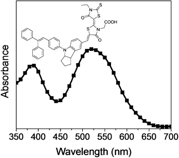 | ||
Fig. 1 The chemical structure and UV absorption spectrum of D149 when it is adsorbed on a thin film of TiO2 from a solution of acetonitrile/tert-butylalcohol (v/v = 1![[thin space (1/6-em)]](https://www.rsc.org/images/entities/char_2009.gif) :1). :1). | ||
Experimental
Materials
All chemicals were used as received with no further purification. Acetic acid and concentrated nitric acid were purchased from Merck. Titanium tetraisopropoxide, tetraethyl ammonium hydroxide, chenodeoxycholic acid, hexachloroplatinic acid, tert-butylalcohol, tetrabutylammonium iodide, lithium perchlorate, 4-tert-butylpyridine and iodine were purchased from Sigma–Aldrich. All solvents used were of AR grade and were obtained from either Sigma–Aldrich or Tedia. FTO glass substrates were from Hartford Glass. Plastic PEN–ITO substrates were purchased from Peccell Technologies. P25 TiO2 nanoparticles were kindly gifted by Degussa. The D149 dye was from Mitsubishi Paper Mills. The 25 μm thick spacer was obtained from Solaronix.Synthesis of TiO2 nanoparticles
The synthesis of the various TiO2 nanoparticles was performed using modified literature procedures.29,30 The general procedure is described as follows and the exact amount of each reagent used is shown in Table 1.| Samples | Crystallite size a | Particle size b | Peptizing agent | Peptization temperature | Peptization time | Post treatment |
|---|---|---|---|---|---|---|
| a According to the Scherrer equation b According to TEM | ||||||
| A | 10 nm | 11 ± 2 nm | 1.2 mL Conc. HNO3 | 200 °C | 12 h | 1.2 mL |
| B | 14 nm | 15 ± 2 nm | 1.2 mL Conc. HNO3 | 250 °C | 15 h | 1.2 mL |
| C | 19 nm | 20 ± 3 nm | 3.6 mL Conc. HNO3 | 250 °C | 12 h | 3.6 mL |
| D | 27 nm | 29 ± 4 nm | 22 mL 20 wt% TEAH solution | 200 °C | 5 h | 5.0 mL |
3.6 g (0.06 mol) of CH3COOH was added to 17.6 g of titanium tetraisopropoxide and the mixture was stirred at room temperature for 15 min. The mixture was then poured into 90 mL of deionized water while stirring rapidly to prevent aggregation. The resulting milky white suspension was stirred for 1 h at room temperature. Varying amounts of concentrated HNO3 or tetraethyl ammonium hydroxide (TEAH) were added to prepare TiO2 nanoparticles of different sizes. After that, the suspension was heated to 80 °C and allowed to react for another 75 min. Upon cooling to room temperature, the total volume was made up to 110 mL by adding deionized water. The suspension was transferred to a stainless steel autoclave and heated at varying temperatures and times to yield nanoparticles of different sizes. Upon cooling, varying amounts of concentrated HNO3 were added as a post-treatment step. The mixture was sonicated for 30 min before centrifugation. Deionized water was added to the sediment and the sonication/centrifuge process was repeated as a washing step. The washing process was repeated until the pH of the resulting supernatant reached 7.0. The washing process was then repeated with ethanol 3 times before drying the nanoparticles at 70 °C. The TiO2 flakes were subsequently made into powders by grinding with a mortar and pestle.
Particle characterization
The morphology of TiO2 nanoparticles was studied using a transmission electron microscope (JEOL JEM-2100F). 2–3 mg of TiO2 powder was suspended in 10 mL of ethanol and sonicated for 10 min. A drop of this suspension was casted onto a standard TEM copper grid. The morphology of the TiO2 films was viewed using field emission scanning electron microscopy (FESEM, JEOL) after sputtering with platinum. The crystal structure and crystallite size was determined by X-ray diffraction (Shiamadzu XRD-6000). The working voltage and current were 40 kV and 20 mA, respectively. The powdered sample was placed on an aluminum substrate. The scan rate was set at 2 degrees per minute and the scanning range was set at 10 to 80 degrees. Zeta potential studies on the different suspensions were performed in a DTS1060 capillary cell (Malvern) using a Zetasizer, (Nanoseries, Malvern Instruments, Malvern, U.K.). 1–2 mg of TiO2 nanoparticles were suspended in 10 mL of a mixture of ethanol, isopropanol and butanol (v/v/v = 1:2:4) and sonicated for 30 min. The suspension was acidified with HNO3 until a pH of about 3.0–4.0 was reached before injected into the sample cell using a syringe.
Preparation of photoanodes by EPD
The TiO2 suspension for EPD was prepared by mixing 0.5 g of TiO2 powder with 15 mL of a mixture of ethanol, isopropanol and butanol (v/v/v = 1:2:4), which was followed by ultrasonication for 30 min. Before the EPD process, the colloidal suspension was acidified to a pH of about 3.0–4.0 with HNO3. A pair of FTO glass substrates (2 cm × 2.5 cm, 15 Ω sq−1) or plastic PEN–ITO substrates (2 cm × 2.5 cm, 15 Ω sq−1) were vertically immersed in the suspension. The distance between each pair of substrates was kept at 7 mm and the DC power supply was set at 30 V for a constant voltage during the EPD process. The thickness of the resulting film was controlled by the deposition time. The freshly coated films were left to dry in air before being heated at 100 °C for 30 min to enable low temperature annealing and to ensure all the solvent from the EPD process was removed.
DSSC assembly
The prepared photoanodes were subsequently subjected to a pressure of 1 ton cm−2 (Atlas Manual 15T Hydraulic Press) for 2 min to improve the interparticle adhesion and electrical connectivity.11 As a result of the pressing process, the thickness of the films was reduced. The photoanodes were heated at 70 °C for 30 min before immersion in a 0.5 mM D149 dye solution in acetonitrile/tert-butylalcohol (v/v = 1:1) with 0.5 mM chenodeoxycholic acid as a co-adsorbant for 2 h. The photoanodes were subsequently rinsed with acetonitrile and left to dry in the dark.
The rigid Pt counter electrode was prepared by spin-coating a 30 mM H2PtCl6 solution in isopropanol on a FTO glass substrate, followed by thermal decomposition at 400 °C for 15 min. The flexible Pt counter electrode was fabricated by sputtering Pt (20 mA for 120 s) on the PEN–ITO substrate using a JEOL JFC-1600 Auto Fine Coater. DSSCs were fabricated by sandwiching a TiO2 photoanode and a Pt counter electrode with the electrolyte in a 25 μm thick spacer. The electrolyte used had a composition of 0.5 M tetrabutylammonium iodide, 0.001 M LiClO4, 0.5 M 4-tert-butylpyridine and 0.1 M I2 in 3-methyoxypropionitrile. The active area of the cell was 0.16 cm2, which was controlled by a metal mask.
Determination of the dye loading
A TiO2 film was prepared on a glass substrate by EPD as described above. An area of 30 mm2 (5 mm × 6 mm) was immersed in a D149 dye solution of 0.5 mM in acetonitrile/tert-butylalcohol (v/v = 1:1) with 1 mM chenodeoxycholic acid as a co-adsorbant for 2 h. The sensitized photoanode was soaked in a solution of ammonia in DMSO (0.1 M) for 30 min for dye desorption. After complete desorption, the UV–vis absorption spectrum (Shimadzu) of the resultant solution was measured at 526 nm, the absorption maximum of the dye. The dye loading was calculated from the molar extinction coefficient of D149 (6.8 × 10⁴ M−1cm−1 at 526 nm) using Beer–Lambert's law. The dye loading data reported were an average of 3 samples.
Photovoltaic measurements
The photovoltaic parameters of the DSSCs were studied by an AutoLAB PGSTAT 320 N potentiostat with simulator light (AM 1.5G, 100 mWcm−2). The intensity modulated photocurrent spectroscopy (IMPS) and intensity modulated photovoltage spectroscopy (IMVS) measurements were carried out using an AutoLAB PGSTAT 320 N potentiostat with a green light emitting diode (λ = 530 nm).Results and discussion
Four different batches of TiO2 nanoparticles were synthesized by varying the reaction temperature, reaction time and peptization agent. The transmission electron microscopy (TEM) images of the synthesized nanoparticles are shown in Fig. 2. The nanoparticles have a slightly elongated shape. The average particle size under TEM is determined by measuring and averaging both the long and short end-to-end distances of dozens of particles. The sizes of the nanoparticles estimated from the TEM images were 11 ± 2, 15 ± 2, 20 ± 3 and 29 ± 4 nm, which indicate that longer peptization times and higher peptization temperatures lead to larger nanoparticles. X-Ray diffraction (XRD) was performed to determine the crystal phase of the synthesized TiO2 nanoparticles. Fig. 3 shows that all the synthesized nanoparticles are in the pure anatase crystal phase. From the XRD results, the crystallite sizes of the synthesized nanoparticles are 10, 14, 19 and 27 nm, which were determined based on the (101) peaks (2θ = 25.3°) using the Scherrer equation: | (1) |
where τ is the crystallite size (in Å), λ is the wavelength of radiation used (1.54056 Å for Cu–Kα1), β is the width of the peak at half maximum intensity (in radians) and θ is the diffracted angle at maximum intensity (in radians). The crystallite sizes calculated from the Scherrer equation generally agree with that observed by TEM. The crystallite size of the nanoparticles determined via the Scherrer equation and the nanoparticle size determined using TEM are summarized in Table 1.
 | ||
| Fig. 2 TEM images of the synthesized TiO2 nanoparticles. (A) ∼10 nm, (B) ∼14 nm, (C) ∼19 nm and (D) ∼27 nm. The scale bars represents 50 nm. | ||
 | ||
| Fig. 3 XRD spectra of TiO2 nanoparticles. (A) ∼27 nm, (B) ∼19 nm, (C) ∼14 nm and (D) ∼10 nm. The peaks of anatase are labelled. No change was observed after compression at 1 ton cm−2. | ||
The synthesized nanoparticles, after treatment with acid, have zeta potentials of ∼ +25 mV in the alcohol mixture (n-butanol:isopropanol:ethanol v/v/v = 4:2:1) used in the EPD process. The charge present on the TiO2 nanoparticles is pH dependent and, under acidic conditions, positive charges are induced.31 Due to the positive charges present on the nanoparticle surface, the colloidal suspensions are relatively stable during the EPD process. As EPD utilizes electrostatic attraction for particle deposition, the positive charge favors their direct utilization in the EPD process without any further additives or surface modifications, which are common required for particles lacking surface charges.32
The films made from EPD followed by a compression process were mechanically stable and robust. The film, when formed on a flexible plastic substrate, can be bent easily without mechanically destroying the film. This is unlike unprocessed EPD films that need to be handled delicately in order to preserve the mechanical integrity of the film. To study the difference in film morphology brought about by compression, the films before and after compression were viewed by FESEM. Fig. 4A shows clearly that the unpressed EPD film fabricated from 19 nm TiO2 nanoparticles had visible micropores and the interparticle connectivity was poor. After compression, however, it can be clearly seen in Fig. 4B that the interparticle connection has been improved and less interparticle pores are observed. The FESEM images indicate that compression treatment can reduce local interparticle pores and improve interparticle connectivity. In addition, the film thickness was reduced by the compression process, indicating that void spaces within the uncompressed film have been significantly reduced and the nanoparticles within the film are in closer contact after compression. The films fabricated using the other nanoparticles showed the same observations as well. In addition to the FESEM studies, the effect of compression on the crystal phase of the particles was also studied. XRD did not show any change in crystal phase and crystallite size in the pressed samples.
 | ||
| Fig. 4 FESEM images of (A) as prepared EPD films from 19 nm TiO2 nanoparticles. (B) After compression. The scale bars represents 100 nm. | ||
The devices have a sandwiched structure in which the D149 sensitized photoanode and the Pt counter electrode are clipped together. A 25 μm spacer (Solaronix) was used to prevent the short circuiting of the cell. A few drops of the electrolyte, containing 0.5 M tetrabutylammonium iodide, 0.001 M LiClO4, 0.5 M 4-tert-butylpyridine and 0.1 M I2 in 3-methyoxypropionitrile, was introduced to complete the cell assembly.
The effect of the TiO2 film thickness on the device performance was first investigated for the nanoparticles. The post compression thickness was controlled and set to be ∼4, ∼8, ∼11 and ∼15 μm. The changes in the open circuit voltage (Voc), the short-circuit current density (Jsc), the fill factor (FF) and the overall efficiency (η) with the TiO2 film thickness are shown in the ESI (Tables S1–S4†).
The best performing devices fabricated using different TiO2 nanoparticles have different TiO2 thicknesses. For 10 nm and 14 nm nanoparticles, their corresponding devices performed optimally at a post compression film thickness of ∼8 μm. For the larger 19 nm and 27 nm nanoparticles, the optimal film thickness was ∼11 μm. The J–V curves of the best performing devices for each individual set of nanoparticles are shown in Fig. 5 and the corresponding photovoltaic parameters are shown in Table 2. For the optimized devices, the Voc of the devices increased from 0.77 to 0.85 V when the nanoparticle size was increased from 10 nm to 27 nm. The Jsc of the devices increased from 10.6 to 14.3 mA cm−2 when the nanoparticle size was increased from 10 nm to 19 nm. When the size of the nanoparticles was further increased to 27 nm, the Jsc decreased to 9.2 mA cm−2. The FF of the devices was between 0.63 to 0.68. The best performing devices fabricated using 10, 14, 19 and 27 nm nanoparticles yielded efficiencies of 5.3%, 5.4%, 7.0% and 5.3%, respectively.
 | ||
| Fig. 5 J–V curves for the best performing DSSCs fabricated on rigid glass substrates by the EPD technique with compression post treatment. | ||
| Particle size (nm) | Film thickness (μm) | Zeta potential a (mV) | Photovoltaic properties b | Dye loading c (×10−7 mol cm−2) | |||
|---|---|---|---|---|---|---|---|
| V oc (V) | J sc (mA cm−2) | FF | ECE (%) | ||||
|
a Measured in a mixture of ethanol, isopropanol and butanol (v/v/v = 1:2:4)
b Measured under AM 1.5G (100 mWcm−2)
c UV absorbance is measured in 0.1 M of aqueous NH3 in DMSO
|
|||||||
| 10 | 8 | 26.1 | 0.77 | 10.6 | 0.64 | 4.8 | 2.5 |
| 14 | 8 | 24.7 | 0.79 | 10.7 | 0.63 | 5.4 | 1.4 |
| 19 | 11 | 24.0 | 0.79 | 14.3 | 0.65 | 7.0 | 1.3 |
| 27 | 11 | 24.9 | 0.85 | 9.2 | 0.68 | 5.3 | 0.9 |
The Voc of a device is determined by a number of factors,33 namely the Quasi Fermi level of the semiconductor, the HOMO level of the redox couple (Eredox), the light harvesting and electron injection of the sensitizer and the frequency of recombination events within the cell. Since the semiconductor, sensitizer and electrolyte used in this study are the same for all devices, the Voc trend cannot be attributed to Eredox and the identity of the dye. This leaves the recombination rate as the likely reason for such an observed Voc trend.
To understand the observed trend for the Voc of the devices made from different nanoparticles, intensity-modulated photovoltage spectroscopy (IMVS) was performed. The electron lifetime (τn) was calculated from the equation τn = 1/(2πfn,min), where fn,min is the characteristic frequency at the minimum of the IMVS imaginary component.34 As shown in Fig. 6A, the electron lifetime increased from 5.7 ms to 10 ms when the nanoparticle size was increased from 10 nm to 27 nm. As the electron lifetime calculated from the IMVS results is an indication of the number of recombination events, the longer electron lifetime for DSSCs with 27 nm nanoparticles as compared to that with 10 nm nanoparticles indicated that devices fabricated with larger particles undergo less recombination events.24 The IMVS results indicate that electron recombination has been reduced when larger nanoparticles are used and this contributes to a higher Voc for the corresponding devices.
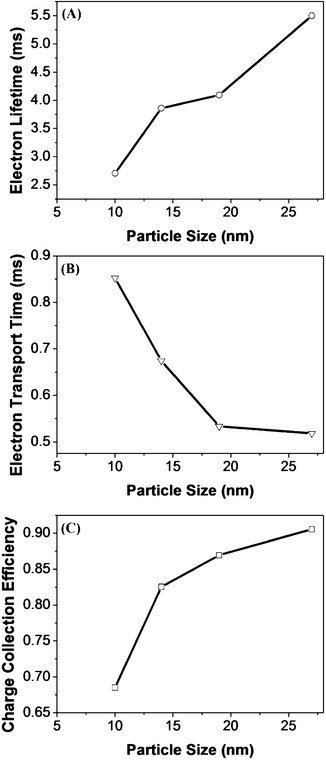 | ||
| Fig. 6 (A) Electron lifetime, (B) electron transport time and (C) charge collection efficiency for thickness-optimized DSSCs fabricated with different sizes of TiO2 nanoparticles. | ||
To check the contribution of dye loading on Jsc for each device, the desorbed dye solutions were measured with UV absorption spectroscopy and the results are summarized in Table 2. It was found that the nanoparticle size influences the dye loading significantly in our devices. For the thickness-optimized devices, the dye loading decreases from 2.5 to 0.9 × 10⁻⁷ M cm−2 when the nanoparticle size is increased from 10 nm to 27 nm. Though the dye loading is related to the device's ability to absorb incident light, the Jsc trend of the devices differs from the dye loading trend. This indicates that the dye loading of the devices is not the sole determinant of the Jsc and the overall device conversion efficiency.
In addition to the dye loading, the electron transport within the TiO2 network could also play a part in determining the Jsc of the devices. To understand the electron transport within the photoanode fabricated from the differently sized TiO2 nanoparticles at their optimal thicknesses, intensity modulated photocurrent spectroscopy (IMPS) was performed on the devices fabricated using the synthesized nanoparticles. The electron transport time (τd) was calculated from the equation τd = 1/(2πfd,min), where fd,min is the characteristic frequency at the minimum of the IMPS imaginary component.34 As shown in Fig. 6B, the electron transport time decreases from 3.2 to 1.2 ms when the nanoparticle size is increased from 10 nm to 27 nm. The electron transport time is a measure of the average time taken for the collection of injected electrons and a faster electron time is associated with a higher photocurrent as it indicates that electrons hop across the TiO2 network and are collected at the photoanode at a faster rate.35
From the calculated τd and τn, the charge collection efficiency can be calculated using the equation: ηc = 1 − τd/τn.36 The calculated values of ηc are shown in Fig. 6C. The charge collection efficiency of the devices increased from 0.46 to 0.88 when the TiO2 nanoparticle size is increased from 10 to 27 nm. The improvement of the charge collection efficiency with the nanoparticle size can be explained using the electron trapping/detrapping model.37–39 Larger nanoparticles have both a lower surface area and a smaller number of grain boundaries, which lead to less electron trapping and is beneficial for a high Jsc and Voc.35–37 Although the charge collection efficiency data predicts that the 27 nm TiO2-based devices should have the highest photocurrent, this is not the case for the Jsc in these devices and this indicates that the charge collection efficiency alone is not indicative of the overall device performance.
From the above studies, it is clear that the device performance is dependent on the optimization of the charge collection efficiency and the dye loading. Small nanoparticles have a higher dye loading for a fixed film thickness and, hence, thinner films can be used for devices fabricated with 10 and 14 nm TiO2. However, devices fabricated with small nanoparticles exhibit poor charge transport properties and this results in a poor Jsc. An increasing particle size decreases the dye loading and increases the film thickness required for optimal performance. However, devices fabricated with larger particles show improved charge collection efficiencies. Since the films used in this study are not sintered, the thickness for which a crack-free film can be fabricated is limited and the requirement for thick crack-free films cannot be fulfilled when the large 27 nm nanoparticles are used. In our results, a moderate nanoparticle size of 19 nm shows the best efficiency. This is ascribed to the 19 nm-based devices' relatively high dye loading, as well as the good charge collection efficiency.
For comparison purposes, a device was fabricated with commercially available Degussa P25 TiO2 nanoparticles. Using the same fabrication method, P25 was deposited via EPD and used as a photoanode in DSSCs. The change in the photovolatic parameters with the film thickness is shown in Table S5† in the ESI. The optimal post compression thickness is found to be ∼ 11 μm. FESEM images of the film before and after compression are shown in Fig. S1† in the ESI.
Flexible DSSCs were fabricated with 19 nm and P25 nanoparticles. The post compression thickness of the TiO2 films was controlled and set to be ∼ 11 μm, which is the optimal thickness for both 19 nm and P25 devices. DSSCs with 19 nm nanoparticles as the photoanode have a Voc of 0.80 V, a Jsc of 10.3 mAcm−2, a FF of 0.62 and an overall efficiency (η) of 5.2%. P25-based devices have a Voc of 0.79 V, a Jsc of 9.32 mAcm−2, a FF of 0.60 and an overall efficiency (η) of 4.5%. When compared to the devices on rigid glass substrates, the efficiency is lower. This is mainly due to the drop in the photocurrent and FF, which is caused by the lower light transmittance and higher electrical resistance in the plastic substrate when compared to glass substrates.40,41
To compensate for the loss of light transmission, large submicron TiO2 particles (∼200 nm–300 nm) were subsequently synthesized41 and utilized as a scattering layer to offset the light loss caused by the plastic substrate. Based on an identical deposition method, a 2 μm scattering layer was deposited on top of the nano-sized TiO2 particles. The J–V curves of these devices are shown in Fig. 7. As such, the efficiency of the devices is significantly improved. The 19 nm nanoparticle-based devices with the scattering layer have a Voc of 0.80 V, a Jsc of 13.8 mAcm−2, a FF of 0.54 and an overall efficiency (η) of 6.0%. The P25-based device with the scattering layer has a Voc of 0.78 V, a Jsc of 11.5 mAcm−2, a FF of 0.56 and an overall efficiency (η) of 5.2%. The light scattering effect of the large submicron sized nanoparticles is well known to increase the light harvesting and hence the Jsc of the devices. 41,42 This leads to an overall increase in the device efficiency as compared to the devices without the scattering layer. As with the devices on the rigid substrates, the performance of the 19 nm nanoparticle-based devices is superior to that of P25. Upon optimizing the particle size for DSSCs fabricated via EPD, the use of a blocking layer to limit recombination,43,44 UV–O3 treatment to reduce the organic contaminants and an anti-reflection film11 for higher light utilization is expected to further improve the device efficiency.
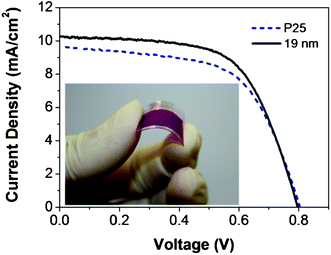 | ||
| Fig. 7 J–V curves for flexible DSSCs fabricated on plastic substrates. 19 nm particles or P25 were used as the mesoporous layer and large particles (∼200–300 nm) were used as light scattering layers. The inset shows a typical TiO2 film, formed by EPD and compression on ITO–PEN, sensitized with the D149 dye. | ||
Conclusions
In this study, TiO2 nanoparticles of sizes 10 nm to 27 nm have been synthesized and used to fabricate DSSCs via the EPD technique. This study has shown that, for low temperature DSSCs fabricated by EPD, the nanoparticle size plays a significant role in determining the device performance. In our devices, the nanoparticle size mainly influences the Jsc of the devices, while the Voc and FF are only mildly affected. IMPS and IMVS studies indicate that the charge collection efficiency increases with the nanoparticle size. At the same time, the dye loading of the devices decreases with the nanoparticle size. Due to a combination of good charge transport properties and relatively high dye loading, 19 nm TiO2 nanoparticle-based devices gave the best device efficiency. Under optimized conditions, we achieved an efficiency of 6.0% on plastic substrates using 19 nm TiO2 nanoparticles with a scattering layer. This is an improvement over the benchmark device made with P25, which achieves an efficiency of 5.2%. These results demonstrate that optimization of the TiO2 nanoparticle size for devices fabricated using the EPD technique is an alternative method to achieve highly efficient plastic dye-sensitized solar cells.Acknowledgements
The authors are grateful to the National Research Foundation of Singapore (NRF-279-000-276-272), IMRE/11-1C0217 and Loreal-Singapore Women in Science National Fellowship 2011 for financial support. Z. Xue thanks the NUS Graduate School for Integrative Sciences and Engineering for financial support via a PhD scholarship. Helpful discussions with Dr X. Liu are also acknowledged.References
- B. O'Regan and M. Grätzel, Nature, 1991, 353, 737–740 CrossRef CAS.
- A. Yella, H. W. Lee, H. N. Tsao, C. Y. Yi, A. K. Chandiran, M. K. Nazeeruddin, E. W. G. Diau, C. Y. Yeh, S. M. Zakeeruddin and M. Grätzel, Science, 2011, 334, 629–634 CrossRef CAS.
- C. M. Chen, C. H. Chen and T. C. Wei, Electrochim. Acta, 2010, 55, 1687–1695 CrossRef CAS.
- S. Ueno and S. Fujihara, J. Electrochem. Soc., 2011, 158, K1–K5 CrossRef CAS.
- S. H. Jang, Y. J. Kim, H. J. Kim and W. I. Lee, Electrochem. Commun., 2010, 12, 1283–1286 CrossRef CAS.
- Y. Kijitori, M. Ikegami and T. Miyasaka, Chem. Lett., 2007, 36, 190–191 CrossRef CAS.
- H. C. Weerasinghe, P. M. Sirimanne, G. P. Simon and Y. B. Cheng, J. Photochem. Photobiol., A, 2009, 206, 64–70 CrossRef CAS.
- D. S. Zhang, T. Yoshida, K. Furuta and H. Minoura, J. Photochem. Photobiol., A, 2004, 164, 159–166 CrossRef CAS.
- D. S. Zhang, T. Yoshida, T. Oekermann, K. Furuta and H. Minoura, Adv. Funct. Mater., 2006, 16, 1228–1234 CrossRef CAS.
- H. Lindstrom, A. Holmberg, E. Magnusson, S. E. Lindquist, L. Malmqvist and A. Hagfeldt, Nano Lett., 2001, 1, 97–100 CrossRef.
- T. Yamaguchi, N. Tobe, D. Matsumoto, T. Nagai and H. Arakawa, Sol. Energy Mater. Sol. Cells, 2010, 94, 812–816 CrossRef CAS.
- L. Yang, L. Q. Wu, M. X. Wu, G. Xin, H. Lin and T. L. Ma, Electrochem. Commun., 2010, 12, 1000–1003 CrossRef CAS.
- H. W. Chen, C. Y. Hsu, J. G. Chen, K. M. Lee, C. C. Wang, K. C. Huang and K. C. Ho, J. Power Sources, 2010, 195, 6225–6231 CrossRef CAS.
- H. W. Chen, C. Y. Lin, Y. H. Lai, J. G. Chen, C. C. Wang, C. W. Hu, C. Y. Hsu, R. Vittal and K. C. Ho, J. Power Sources, 2011, 196, 4859–4864 CrossRef CAS.
- W. H. Chiu, K. M. Lee and W. F. Hsieh, J. Power Sources, 2011, 196, 3683–3687 CrossRef CAS.
- W. W. Tan, X. Yin, X. M. Zhou, J. B. Zhang, X. R. Xiao and Y. Lin, Electrochim. Acta, 2009, 54, 4467–4472 CrossRef CAS.
- X. Yin, X. Z. Liu, L. Wang and B. Liu, Electrochem. Commun., 2010, 12, 1241–1244 CrossRef CAS.
- L. Grinis, S. Dor, A. Ofir and A. Zaban, J. Photochem. Photobiol., A, 2008, 198, 52–59 CrossRef CAS.
- N. Karousis, A. S. D. Sandanayaka, T. Hasobe, S. P. Economopoulos, E. Sarantopoulou and N. Tagmatarchis, J. Mater. Chem., 2011, 21, 109–117 RSC.
- A. Salant, M. Shalom, I. Hod, A. Faust, A. Zaban and U. Banin, ACS Nano, 2010, 4, 5962–5968 CrossRef CAS.
- W. Y. Shi, S. He, M. Wei, D. G. Evans and X. Duan, Adv. Funct. Mater., 2010, 20, 3856–3863 CrossRef CAS.
- I. Corni, M. P. Ryan and A. R. Boccaccini, J. Eur. Ceram. Soc., 2008, 28, 1353–1367 CrossRef CAS.
- T. P. Chou, Q. F. Zhang, B. Russo, G. E. Fryxell and G. Z. Cao, J. Phys. Chem. C, 2007, 111, 6296–6302 CAS.
- L. C. Du, A. Furube, K. Hara, R. Katoh and M. Tachiya, J. Phys. Chem. C, 2010, 114, 8135–8143 CAS.
- R. Katoh, A. Huijser, K. Hara, T. J. Savenije and L. D. A. Siebbeles, J. Phys. Chem. C, 2007, 111, 10741–10746 CAS.
- S. Nakade, Y. Saito, W. Kubo, T. Kitamura, Y. Wada and S. Yanagida, J. Phys. Chem. B, 2003, 107, 8607–8611 CrossRef CAS.
- S. Ito, S. M. Zakeeruddin, R. Humphry-Baker, P. Liska, R. Charvet, P. Comte, M. K. Nazeeruddin, P. Pechy, M. Takata, H. Miura, S. Uchida and M. Grätzel, Adv. Mater., 2006, 18, 1202–1205 CrossRef CAS.
- T. Horiuchi, H. Miura, K. Sumioka and S. Uchida, J. Am. Chem. Soc., 2004, 126, 12218–12219 CrossRef CAS.
- C. J. Barbe, F. Arendse, P. Comte, M. Jirousek, F. Lenzmann, V. Shklover and M. Grätzel, J. Am. Ceram. Soc., 1997, 80, 3157–3171 CrossRef CAS.
- J. H. Kim, W. Y. Jung, S. H. Baek, K. T. Lim, G. D. Lee, S. S. Park and S. S. Hong, Chem. Eng. Sci., 2007, 62, 5154–5159 CrossRef CAS.
- M. Kosmulski, Adv. Colloid Interface Sci., 2002, 99, 255–264 CrossRef CAS.
- N. Koura, T. Tsukamoto, H. Shoji and T. Hotta, Jpn. J. Appl. Phys. Part 1 - Regul. Pap. Short Notes Rev. Pap., 1995, 34, 1643–1647 CAS.
- Z. J. Ning, Y. Fu and H. Tian, Energy Environ. Sci., 2010, 3, 1170–1181 CAS.
- J. Kruger, R. Plass, M. Grätzel, P. J. Cameron and L. M. Peter, J. Phys. Chem. B, 2003, 107, 7536–7539 CrossRef.
- J. van de Lagemaat and A. J. Frank, J. Phys. Chem. B, 2000, 104, 4292–4294 CrossRef CAS.
- G. Schlichthorl, N. G. Park and A. J. Frank, J. Phys. Chem. B, 1999, 103, 782–791 CrossRef.
- J. Nelson, Phys. Rev. B: Condens. Matter, 1999, 59, 15374–15380 CrossRef CAS.
- F. Gracia, J. P. Holgado and A. R. Gonzalez-Elipe, Langmuir, 2004, 20, 1688–1697 CrossRef CAS.
- B. A. Gregg, Coord. Chem. Rev., 2004, 248, 1215–1224 CrossRef CAS.
- X. Z. Liu, Y. H. Luo, H. Li, Y. Z. Fan, Z. X. Yu, Y. Lin, L. Q. Chen and Q. B. Meng, Chem. Commun., 2007, 2847–2849 RSC.
- Z. A. Lan, J. H. Wu, J. M. Lin and M. L. Huang, J. Mater. Sci.: Mater. Electron., 2010, 21, 833–837 CrossRef CAS.
- M. K. Nazeeruddin, A. Kay, I. Rodicio, R. Humphrybaker, E. Muller, P. Liska, N. Vlachopoulos and M. Grätzel, J. Am. Chem. Soc., 1993, 115, 6382–6390 CrossRef CAS.
- E. Palomares, J. N. Clifford, S. A. Haque, T. Lutz and J. R. Durrant, J. Am. Chem. Soc., 2003, 125, 475–482 CrossRef CAS.
- S. Ito, P. Liska, P. Comte, R. L. Charvet, P. Pechy, U. Bach, L. Schmidt-Mende, S. M. Zakeeruddin, A. Kay, M. K. Nazeeruddin and M. Grätzel, Chem. Commun., 2005, 4351–4353 RSC.
Footnote |
| † Electronic Supplementary Information (ESI) available. See DOI: 10.1039/c2ra20542d/ |
| This journal is © The Royal Society of Chemistry 2012 |