Template-assisted synthesis of ordered single crystal InN nanowires†
Zhuo
Chen
*a,
Yanan
Li
a,
Jie
Jiang
a,
Chuanbao
Cao
*a,
Tingting
Xu
b,
Qing
Chen
b,
Xingyan
Xu
a and
Hesun
Zhu
a
aResearch Center of Materials Science, Beijing Institute of Technology, Beijing, 100081, People's Republic of China
bKey Laboratory for the Physics and Chemistry of Nanodevices and Department of Electronics, Peking University, Beijing, 100871, People's Republic of China
First published on 21st May 2012
Abstract
Aligned InN nanowires were synthesized by a template-assisted two-step method. The as-synthesized aligned InN nanowires were of single crystal structure and exhibited good electrical properties with a carrier mobility of 93.8 cm2 V−1 s−1 and a strong photoluminescence emission peak at 740 nm at room-temperature. The alignment characteristic makes it more convenient to integrate the nanowires into nanodevices. The two-step method provides an effective and low-cost road for ordered nitride nanowires in a controllable way.
Introduction
InN as one of the most challenging materials in the III-V nitrides is mainly applied to form alloys with GaN for light emitting diodes and laser diodes. Recently, InN has received considerable attention because of the recent discovery that the band gap is about 0.7 eV,1 rather than the previously accepted 1.9 eV,2 which has generated great interest for applications such as high-efficiency solar cells, light-emitting diodes and laser diodes.3Due to unique chemical and physical properties, one-dimensional (1D) semiconductor nanomaterials not only are interesting for fundamental research, but also offer fascinating potential for future technology applications.4,5 With the recently increasing interest in InN, its 1D nanostructures are also attracting extensive attention. In the year 2000, azido precursor compounds containing the group N3 were used for the synthesis of InN fibers with polycrystallinity by a solution–liquid–solid mechanism.6 InN nanowires have been grown on a gold-patterned silicon substrate by thermal evaporation of pure In foil under NH3 ambience,7 which can be attributed to a Vapor–Liquid–Solid (VLS) growth process. Similarly, InN nanowires have also been obtained by a VLS process using a mixture of In and In2O3 as the starting material.8 Single crystalline InN nanotubes and nanowires have been synthesized by a controlled-carbonitridation reaction route using In2O3 and graphite or multiwalled carbon nanotubes as precursors in a Vapor–Solid (VS) growth process.9 Based on VS growth process, other groups have also reported the preparation of InN nanowires using In or In2O3 as the reaction precursors.10–14 In addition, 1D InN nanostructures have been grown by MBE15–17 and MOCVD.18,19 Although extensive efforts have been devoted to the synthesis and characterization of InN nanowires, the synthesis of ordered InN nanowires in an effective and low-cost way still remains a challenge.
Herein, we report the successful fabrication of aligned InN nanowires via a template assistant two-step method. The as-synthesized aligned InN nanowires were of single crystal structure and exhibited good electrical properties with carrier mobility of 93.8 cm2 V−1 s−1 and a strong photoluminescence emission peak at 740 nm at room-temperature.
Experimental
The ordered single crystal InN nanowires were fabricated by a two-step method. Firstly, indium nanowires were electrodeposited into a polycarbonate (PC) template with 100 nm nanoholes using a standard three-electrode DC electrochemical cell, where Ag/AgCl and Pt were used as the reference electrode and the counter electrode, respectively. A layer of copper was sputtered onto the PC template and it was used as the working electrode before electrodeposition. The electrolyte solution was 0.05 M InCl3 aqueous solution with pH 2 adjusted by diluted HCl. The electrodeposition was carried out for around 15 min at 2 mA cm−2. Then, the PC template with In nanowires (In/PC) was cleaned and dried. The second step was to convert the In nanowires into InN nanowires, which was performed in a tube furnace. In a typical process, the In/PC was placed in the center of the quartz tube under ambient air at 400 °C for 30 min. After the furnace was cooled down to room temperature and purged with Ar gas for 5 min, it was heated to 550 °C and kept at that temperature for 4 h under NH3 at 200 ml min−1.The morphologies and structures of the products were characterized by X-ray diffraction (XRD, Philips X'pert Pro diffractometer), scanning electron microscopy (SEM, Hitachi S–4800) and high-resolution transmission electron microscopy (TEM, Tecnai F30). The photoluminescence spectrum was collected at room temperature with a Hitachi FL-4500 spectrofluorometer. Transport measurements were conducted in situ inside a TEM Tecnai G20 using a Nanofactory TEM-scanning tunneling microscope sample holder.
Results and discussion
The aligned InN nanowires were synthesized through a two-step method combining electrodeposition and a nitridation reaction. The color of the products changed from silver to dark after the nitridation, suggesting that the In nanowires were converted to the InN nanowires. Fig. 1 shows the XRD pattern of the aligned InN nanowires. All the peaks can be indexed to hexagonal InN (JCPDS: 74-0244), except for the two peaks at 2θ = 41° and 2θ = 74.8°, which correspond to cubic Cu4N (JCPDS: 47-1072) and cubic Cu (JCPDS: 03-1018), respectively, due to the Cu electrode.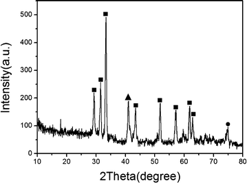 | ||
| Fig. 1 An XRD spectrum of the InN nanowires obtained at 550 °C. ■ – hexagonal phase InN (JCPDS: 74-0244); ▲ – cubic phase Cu4N (JCPDS: 47-1072); ● – cubic phase Cu (JCPDS: 03-1018). | ||
The morphologies of the products were investigated by SEM. From Fig. 2, it can be seen that large scale, vertical or slanted InN nanowires were uniformly obtained in high density on the Cu electrode. The diameters of the InN nanowires are about 200 nm, which depends on the hole size of PC template. This suggests that the diameter, orientation and length of InN nanowires can be controlled by PC or anodic alumina templates and electrodeposition time. Further structural characterization of the InN nanowires was performed by TEM. Fig. 3a shows a TEM image of a InN nanowire. Selected area electron diffraction (SAED) was utilized to investigate the structure and orientation of the synthesized InN nanowires. The SAED pattern confirmed the single crystal nature of the InN nanowire grown along the <100> direction, as shown in Fig. 3b. The high-resolution TEM (HRTEM) image shown in Fig. 3c gives a lattice fringe of about 0.31 nm, corresponding to the d(100) space of the bulk hexagonal InN. Both the SAED pattern and the HRTEM image confirm that the InN nanowires are of excellent crystal quality. The chemical composition of the nanowires was investigated by energy dispersive X-ray spectrum (EDS) analysis, as shown in Fig. 3d. This result confirms that the nanowire is only made of In and N elements, and the ratio of In to N is close to 1![[thin space (1/6-em)]](https://www.rsc.org/images/entities/char_2009.gif) :1. The C and Cu peaks originate from the carbon film and the copper grid, respectively.
:1. The C and Cu peaks originate from the carbon film and the copper grid, respectively.
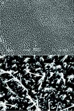 | ||
| Fig. 2 (a and b) SEM images of the ordered InN nanowires. | ||
![(a) TEM image of a InN nanowire. (b) SAED pattern taken along the [001] zone axis. (c) HRTEM image of the nanowire. (d) The EDS spectrum of the nanowire.](/image/article/2012/RA/c2ra20509b/c2ra20509b-f3.gif) | ||
| Fig. 3 (a) TEM image of a InN nanowire. (b) SAED pattern taken along the [001] zone axis. (c) HRTEM image of the nanowire. (d) The EDS spectrum of the nanowire. | ||
Through partial oxidation of the In nanowires before nitridation, we obtained single crystal InN nanowires, which are better than the polycrystalline nanowires obtained through direct nitridation reported by Zhang et al.20 Comparing the partial oxidation and subsequent nitridation process with direct nitridation, the chemical reactions involved are different. In the partial oxidation process, the reaction could be
| In2O3 + 2In + 4NH3 → 4InN + 3H2O + 3H2 | (1) |
In the direct nitridation process, the reaction could be
| 2In + 2NH3 → 2InN + 3H2 | (2) |
By calculation of the Gibbs free energies of the two reactions, one can obtain ΔGr(1) = −247.65 KJ mol−1 and ΔGr(2) = −175.55 KJ mol−1, at 550 °C (for the detailed calculation and thermodynamic data see the ESI† and Ref. 21), which means that the formation of indium oxide is thermodynamically favorable for the nitridation of metal In nanowires. On the other hand, the PC template is burned away after oxidation. It would be helpful for the nitridation of metal In nanowires if the PC template was used to replace anodic aluminium oxide (AAO) because AAO inhibits the nitrogen diffusion. Based on the above analysis, the oxidation at 400 °C plays a key role for improving the crystal quality of InN nanowires.
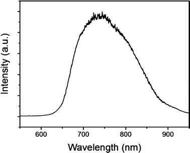
Transport measurements were conducted in situ inside a TEM Tecnai G20 using a Nanofactory TEM-STM sample holder. The vacuum level of the TEM was about 1 × 10⁻⁵ Pa. Fig. 4a shows a TEM image of an InN nanowire of about 135 nm connected to two electrodes, where the top Pt electrode was stationary and the bottom sharp W tip was movable via control of a piezotube with a minimum step of 0.02 nm. Fig. 4b shows an I–V curve with almost symmetric characteristics. A metal–semiconductor–metal model for quantitative analysis of current–voltage characteristics of InN nanowires was applied to fit the experiment data.22,23 Based on this model, one can obtain the intrinsic parameters of the InN nanowires. We measured a total of 7 nanowires. Corresponding I–V, conductivity and carrier concentration curves are displayed in Fig. S1 and S2†, respectively. These nanowires had an average conductivity of 1680.5 (S m−1), an average carrier mobility of 93.8 cm2 V−1 s−1 and an average carrier concentration of 1.22 × 1018 cm−3. The conductivity is similar to the previous values reported by F. Werner,24 C.-Y. Chang25 and T. Richter.26 The carrier concentration is similar the values reported by G. Koley,27 lower than 1.83 × 10²¹ (cm−3) by G. S. Cheng,28 higher than 1014∼1015 (cm−3) by T. Richter.26 The carrier mobility is lower than that reported by G. Koley,27 but higher than 29.2 (cm2 V−1 s−1) reported by G. S. Cheng.28 The mobility is comparable with that of bulk InN on GaN,28 which means that the InN nanowires have a promising potential in future nanoelectronic devices, such as field effect transistors, detectors, and solar cells. The room-temperature photoluminescence emission spectrum of the aligned InN nanowires was obtained using a Xe lamp with excitation at 325 nm as shown in Fig. 5. A strong emission peak was observed at 740 nm in the range of 650–900 nm. The emission wavelength of 740 nm corresponds to a bandgap of about 1.68 eV, in agreement with the reported results for InN nanowires. The high energy and the broad emission peak are probably associated with defects and oxygen impurities.
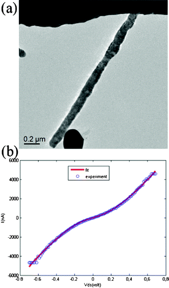 | ||
| Fig. 4 Two-terminal I–V measurements of an InN nanowire. (a) TEM image showing the M–S–M structure; (b) an almost symmetric I–V curve. The circles are experimental I–V data, and the solid lines are fitted theoretical curves. | ||
Conclusions
The ordered single crystal InN nanowires were fabricated by a two-step method. Through partial oxidation of In nanowires before nitridation, we obtained single crystal InN nanowires. The results obtained by XRD, SAED, and HRTEM indicated that the InN nanowires grew along the [100] direction and exhibited an excellent crystal quality. Transport measurements of the InN nanowires were conducted in situ inside a TEM. The average intrinsic parameters of the InN nanowires, i.e., conductivity (1680.5 S m−1), carrier mobility (93.8 cm2 V−1 s−1) and doping concentration (1.22 × 1018 cm−3) were obtained, which means that the InN nanowires have a promising potential in future nanoelectronic devices. The room-temperature PL spectrum exhibited a strong emission peak at 740 nm in the range of 650–900 nm, which is probably associated with defects and oxygen impurities.Acknowledgements
This work was financially supported by the National Natural Science Foundation of China (Grant No. 51102017, 50972017 and 60925003) and the Science Foundation for the Excellent Youth Scholars of Beijing Institute of Technology (Grant No. 2011YC0902).References
- B. Monemar, P. P. Paskov and A. Kasic, Superlattices Microstruct., 2005, 38, 38–56 CrossRef CAS.
- S. Strite and H. Morkoc, J. Vac. Sci. Technol., B, 1992, 10, 1237–1266 CAS.
- B. Ashraful Ghani, H. Akihiro and Y. Akio, J. Appl. Phys., 2003, 94, 2779–2808 CrossRef.
- J. Hu, T. W. Odom and C. M. Lieber, Acc. Chem. Res., 1999, 32, 435–445 CrossRef CAS.
- M. Law, J. Goldberger and P. Yang, Annu. Rev. Mater. Res., 2004, 34, 83–122 CrossRef CAS.
- S. D. Dingman, N. P. Rath, P. D. Markowitz, P. C. Gibbons and W. E. Buhro, Angew. Chem., Int. Ed., 2000, 39, 1470–1472 CrossRef CAS.
- C. H. Liang, L. C. Chen, J. S. Hwang, K. H. Chen, Y. T. Hung and Y. F. Chen, Appl. Phys. Lett., 2002, 81, 22–24 CrossRef CAS.
- T. Tang, S. Han, W. Jin, X. Liu, C. Li, D. Zhang, C. Zhou, B. Chen, J. Hanand and M. Meyyapan, J. Mater. Res., 2004, 19, 423 CrossRef CAS.
- L.-W. Yin, Y. Bando, D. Golberg and M.-S. Li, Adv. Mater., 2004, 16, 1833–1838 CrossRef CAS.
- Z. H. Lan, W. M. Wang, C. L. Sun, S. C. Shi, C. W. Hsu, T. T. Chen, K. H. Chen, C. C. Chen, Y. F. Chen and L. C. Chen, J. Cryst. Growth, 2004, 269, 87–94 CrossRef CAS.
- M. C. Johnson, C. J. Lee, E. D. Bourret-Courchesne, S. L. Konsek, S. Aloni, W. Q. Han and A. Zettl, Appl. Phys. Lett., 2004, 85, 5670–5672 CrossRef CAS.
- S. Vaddiraju, A. Mohite, A. Chin, M. Meyyappan, G. Sumanasekera, B. W. Alphenaar and M. K. Sunkara, Nano Lett., 2005, 5, 1625–1631 CrossRef CAS.
- H. Y. Xu, Z. Liu, X. T. Zhang and S. K. Hark, Appl. Phys. Lett., 2007, 90, 113105 CrossRef.
- S. Luo, W. Zhou, Z. Zhang, L. Liu, X. Dou, J. Wang, X. Zhao, D. Liu, Y. Gao, L. Song, Y. Xiang, J. Zhou and S. Xie, Small, 2005, 1, 1004–1009 CrossRef CAS.
- T. Stoica, R. J. Meijers, R. Calarco, T. Richter, E. Sutter and H. Luth, Nano Lett., 2006, 6, 1541–1547 CrossRef CAS.
- T. Stoica, R. Meijers, R. Calarco, T. Richter and H. Luth, J. Cryst. Growth, 2006, 290, 241–247 CrossRef CAS.
- H. Y. C. C. H. Shen, H. W. Lin, S. Gwo, A. A. Klochikhin and V. Yu, Appl. Phys. Lett., 2006, 88, 253104 CrossRef.
- O. K. J. Mangum, H. J. Park, T. J. Anderson and Z. Liliental-Weber, ECS Trans., 2007, 8, 131 CrossRef.
- O. Kryliouk, H. J. Park, Y. S. Won, T. Anderson, A. Davydov, I. Levin, J. H. Kim and J. A. Freitas Jr, Nanotechnology, 2007, 18, 135606 CrossRef.
- J. Zhang, B. Xu, F. Jiang, Y. Yang and J. Li, Phys. Lett. A, 2005, 337, 121–126 CrossRef CAS.
- O. Kubaschewski, C. B. Alcock and P. J. Spencer, Materials Thermochemistry, Pergamon Press, Oxford 1993 Search PubMed.
- Z. Y. Zhang, C. H. Jin, X. L. Liang, Q. Chen and L. M. Peng, Appl. Phys. Lett., 2006, 88, 073102 CrossRef.
- Z. Y. Zhang, K. Yao, Y. Liu, C. H. Jin, X. L. Liang, Q. Chen and L. M. Peng, Adv. Funct. Mater., 2007, 17, 2478–2489 CrossRef CAS.
- F. Werner, F. Limbach, M. Carsten, C. Denker, J. Malindretos and A. Rizzi, Nano Lett., 2009, 94, 1567–1571 CrossRef.
- C.-Y. Chang, G.-C. Chi, W.-M. Wang, L.-C. Chen, K.-H. Chen, F. Ren and S. J. Pearton, Appl. Phys. Lett., 2005, 87, 093112 CrossRef.
- T. Richter, H. Luth, Th. Schapers, R. Meijers, K. Jeganathan, S. Est'evez Hern'andez, R. Calarco and M. Marso, Nanotechnology, 2009, 20, 405206 CrossRef CAS.
- G. Koley, Z. Cai, E. B. Quddus, J. Liu, M. Qazi and R. A. Webb, Nanotechnology, 2011, 22, 295701 CrossRef.
- G. S. Cheng, E. Stern, D. T. Evans and M. A. Reed, Appl. Phys. Lett., 2005, 87, 253103 CrossRef.
Footnote |
| † Electronic Supplementary Information (ESI) available. See DOI: 10.1039/c2ra20509b/ |
| This journal is © The Royal Society of Chemistry 2012 |