Rapid synthesis of Zn2+ doped SnWO4 nanowires with the aim of exploring doping effects on highly enhanced visible photocatalytic activities†
Yiguo
Su
,
Lichun
Hou
,
Chunfang
Du
,
Liman
Peng
,
Kai
Guan
and
Xiaojing
Wang
*
College of Chemistry and Chemical Engineering, Inner Mongolia University, Hohhot, Inner Mongolia 010021, P. R. China. E-mail: wang_xiao_jing@hotmail.com; Fax: +86-471-4992981; Tel: +86-471-4344579
First published on 8th May 2012
Abstract
In this work, we report on the rapid synthesis of Sn1−xZnxWO4 nanocrystals with the aim of tailoring their structural, electronic, and photocatalytic properties. The samples were carefully characterized by X-ray diffraction, transmission electron microscopy, inductive coupled plasma optical emission spectroscopy, UV-vis diffuse reflectance spectroscopy, and the Barrett–Emmett–Teller technique. The effects of Zn2+ doping in SnWO4 on the electronic structure and photogradation of methylene orange dye solution were investigated experimentally and theoretically. It was found that Zn2+ ions were homogeneously incorporated into the SnWO4 host lattice with a solubility of x = 0.060, which led to a monotonous decrease in lattice volume. With Zn2+ doping, SnWO4 nanocrystals showed a morphological alteration from irregular nanosheets to nanowires. Meanwhile, the BET surface areas were also greatly enlarged from 54 m2 g−1 to ∼100 m2 g−1. Contrary to the theoretical predictions of the quantum size effect, Zn2+ doped SnWO4 nanocrystals showed an abnormal band gap narrowing, which can be well-defined as a consequence of the balance of quantum size effect, lattice contraction, electronegativity, and surface defect centers. With well-controlled morphology, surface area, and electronic structure via Zn2+ doping, the photocatalytic performance of Sn1−xZnxWO4 nanocrystals was optimized at a Zn2+ doping level of x = 0.045.
Introduction
Introducing impurity ions into a semiconducting host, in order to control its structure, particle size, morphology, surface features and chemical composition, has been one of the most important techniques since the necessity arose for tailored properties with promising applications in electronics, magnetics, light emitting devices and catalysis.1 In this regard, semiconductors doped with metal or non-metal ions showing visible photocatalytic activity have attracted great interest, because they provide a potential solution to many environmental pollution problems that humankind is currently facing.2To significantly improve the visible photocatalytic efficiency of oxide semiconductors (e.g. TiO2 and NaTaO3), one can tailor the particle sizes, morphologies, band gap energies and surface active sites by modifying the host structures with various transition metal dopants including La, Fe, Cu, and Bi.3 However, doping strategies have shown both positive and negative impacts for most of the semiconductors. This is because there exist very complicated factors, such as particle size, electronic structure, dopant concentration, surface area, d electronic configuration of transition ions, and the localized d-levels of dopants, which could contribute to the photocatalytic activity. For instance, the localized d-levels of transition metal dopants can not only decrease the photothreshold energy but also serve as recombination centers for photoinduced charge carriers.4 Apparently, clarifying the correlation between these factors and photoactivity is fundamentally important, which may facilitate the design and exploitation of novel photocatalysts showing efficient visible-light response.
Herein, multi-metal oxide semiconductors were taken as the model compounds based on the following considerations: (1) in comparison to traditional binary oxides (e.g. TiO2, ZnO and SnO2et al.), multi-metal oxide semiconductors possess higher tolerance to structural distortion due to their inherent lattice strain, which enables the incorporation of foreign ions into the host matrix;5 (2) the multi-metal oxides show higher chemical stability and fewer electron–hole pair recombination centers, so that charge carrier separation and migration is more effective;4b (3) multi-metal oxides, such as SnWO4, Sn2Ta2O7, Cd2Sb2O6.8etc. are excellent visible-light driven photocatalysts, which provide a convenient way to obtain doped materials with highly enhanced visible photocatalytic activities.6 As a multi-oxide, SnWO4 offers a better environmentally visible-light driven alternative to the oxides containing harmful and expensive ions. Though bulk SnWO4 exhibits superior photocatalytic activity to that of the nanosized WO3 and TiONx, the nano-chemistry of SnWO4 is still limited by the difficulties associated with conventional solid-state synthesis.6a With the aim of using visible-light to generate electron–hole pairs for promoting photocatalytic reactions, it is desirable to exploit a SnWO4 based photocatalyst with a well-defined phase structure, particle size, and surface area, by a rapid, reproducible and simple method.
In this work, we report on the fabrication of Zn2+ doped α-SnWO4 nanocrystals by a rapid and simple microwave-assisted hydrothermal approach. The doping effects were systematically studied in an attempt to investigate the possible reasons for the significantly improved photocatalytic activity toward the degradation of methylene orange.
Experimental section
Sample preparation
All chemicals were of analytical grade and were used without further purification. All samples were prepared in a microwave system (NOVA-1, PreeKem Scientific Instruments Co., Ltd.). The system was equipped with in situ magnetic stirring. The exposure time and temperature were programmed. The automatic temperature-control system allowed continuous monitoring and control of the internal temperature of the reaction system (1 °C). A typical synthetic procedure for Sn1−xZnxWO4 (the initial molar ratios of Zn to Sn were 0, 0.02, 0.05, 0.07, 0.10 and 0.12) nanocrystals can be described briefly as follows: 1.0 mmol SnCl2·2H2O and a given amount of ZnCl2 were dissolved in 10 mL degassed water. Na2WO4 aqueous solution (0.1 M, 15 mL) was added dropwise to the above solution under continuous stirring. A well controlled NaOH solution was used to adjust the pH value to 7. After treating the mixture at 180 °C for 10 min under microwave irradiation, it was rapidly cooled to room temperature by an air compressor. The obtained products were washed with distilled water several times and dried at 80 °C for 3 h.Sample characterization
The phase purities of all samples were characterized by X-ray power diffraction (XRD) on a Rigaku DMAX2500 X-ray diffractometer using a copper target. The average grain size, D, was measured from the diffraction peak (121) using the Scherrer formula, D = 0.9 λ/(βcosθ), where λ is the X-ray wavelength employed, θ is the diffraction angle of the diffraction peak (121), and β is defined as the half width after subtracting the instrumental broadening. The particle sizes and morphologies of the samples were determined using transmission electron microscopy (TEM) on a JEM-2010 apparatus with an acceleration voltage of 200 kV. The chemical compositions of the samples were measured by the inductively coupled plasma (ICP) technique on a Perkin-Elmer Optima 3300DV spectrometer. Optical diffuse reflectance spectra of the samples were measured using a UVIKON XL/XS Spectrometer at room temperature. The specific surface areas of the samples were determined from the nitrogen absorption data at liquid nitrogen temperature by using the Barrett–Emmett–Teller (BET) technique on a Micromeritics ASAP 2000 Surface Area and Porosity Analyzer.The plane-wave based density functional theory (DFT) calculations of the Sn1−xZnxWO4 samples were performed with the CASTEP program package with the core orbitals replaced by ultrasoft pseudopotentials, the generalized gradient approximation (GGA) with the Perdew, Burke and Emzerhof (PBE) exchange correlation functional, and a kinetic energy cutoff of 450 eV. Ninety-six atom supercells were constructed in order to explore the doping effects by 2 × 2 × 2 expansion of the unit cell of α-SnWO4. The Broyden, Fletcher, Goldfarb, and Shannon minimization was used to perform the structural optimization and the convergence. All band structures and the density of states were calculated on the corresponding optimized crystal geometries.
Photocatalytic activity test
A heteropolyaromatic dye, methylene orange dye (MO), was used as a probe molecule to evaluate the photocatalytic reactivity of the samples in response to visible light at room temperature. The experiments were carried out as follows: 50 mg of the sample was placed in 50 mL 2 × 10⁻⁵ M MO aqueous solution in a 100 mL beaker. Prior to illumination, the suspension was magnetically stirred in the dark for 12 h to ensure the establishment of an absorption–desorption equilibrium of MO on the sample surface. Subsequently, the suspension was irradiated under a 300 W Hg lamp with a filter (λ ≥ 420 nm) as a cutoff, about 10 cm away from the beaker. At given intervals, 5 mL of the suspension was extracted and subsequently centrifuged at a rate of 8000 rpm for 10 min. UV-vis absorption spectra of the supernatant were then measured with a UVIKON XL/XS Spectrometer.Results and discussion
Fig. 1 shows X-ray diffraction patterns of the Sn1−xZnxWO4 nanocrystals prepared by a microwave-assisted hydrothermal approach. It is found that, by varying the dopant concentration x ≤ 0.10, XRD data of all diffraction peaks could be accurately indexed to a pure orthorhombic phase of α-SnWO4 (Joint Committee on Powder Diffraction Standards, JCPDS card, No. 29-1354). Upon further increasing the Zn2+ content up to x = 0.12, several additional sharp diffraction peaks appeared, which are assigned to an unknown phase with a large domain size (Fig. S1, ESI†), showing the same XRD pattern as that of the cubic Sn2TiWO7 (25-0978). The broad diffraction peaks indicate the fine crystalline nature of Sn1−xZnxWO4. The peak broadening was used to calculate the crystalline size of the primary particles. Based on the half height width of the (121) peak, the particle size was calculated to be around 9.7 nm for pure SnWO4 and 5.6–6.0 nm for Sn1−xZnxWO4 (x ≤ 0.10) nanocrystals, respectively.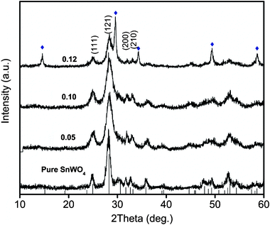 | ||
| Fig. 1 XRD patterns of Sn1−xZnxWO4 nanocrystals with initial dopant concentration. The vertical bars below the patterns represent the standard diffraction data from the JCPDS file for α-SnWO4 (29-1354). | ||
To prove the presence of Zn2+ in SnWO4 nanocrystals, chemical analyses of the as-prepared samples were performed by the inductively coupled plasma-atomic emission spectrometry (ICP-AES) technique. As indicated in Fig. 2, the final molar ratios of Zn2+ content in Sn1−xZnxWO4 nanocrystals were all smaller than the initial ones. Increasing the initial Zn2+ concentration causes the Zn2+ content in the final samples to increase. The maximum dopant concentration of Zn2+ is about 0.060. The inset of Fig. 2 illustrates the X-ray photoelectron spectroscopy (XPS) data of Zn for Sn1−xZnxWO4 (x = 0.060). The XPS spectrum of Sn1−xZnxWO4 in the Zn 2p region shows the binding energies of Zn 2p3/2 and Zn 2p1/2 at around 1021.7 and 1043.9 eV, respectively, suggesting that Zn exists in the chemical state of Zn2+ in Sn1−xZnxWO4 nanocrystals.7 Moreover, the chemical states of Sn and W were also determined to be Sn2+ and W6+ by XPS data (Fig. S2, ESI†).8 To further specify the homogeneous incorporation of Zn2+ into the SnWO4 host matrix, the variations of the lattice parameters for Sn1−xZnxWO4 are supposed to be investigated. By a least-squares method using the Retica Rietveld program (Version LHPM, 2000, B. A. Hunter and C. J. Howard, Lucas Heights Research Laboratories, Menai 2234, Australia), the lattice volumes were determined. Fig. 3 shows the lattice parameters of Sn1−xZnxWO4 nanocrystals as a function of dopant concentration of Zn2+. Upon varying the Zn2+ doping level from x = 0 to 0.060, a lattice contraction was observed, as indicated by the monotonous decrease in lattice volume. It is then highly necessary to clarify the occupation-site of the dopant Zn2+ in SnWO4 nanocrystals. It is much easier to substitute Zn2+ into Sn2+ rather than W6+ sites, because (1) the Pauling electronegativity of Zn2+ is 1.58, close to 1.34 for Sn2+ but much smaller than that of 2.03 for W6+;9 (2) the ionic radius for Zn2+ is 0.74 Å in 6-fold coordination, smaller than that of 1.18 Å for Sn2+, while Zn2+ in 4-fold coordination has an ionic radius of 0.6 Å, larger than that of 0.42 Å for W6+;10 (3) there exists a huge charge difference between Zn2+ and W6+. If Zn2+ was doped at the W6+ sites in SnWO4, then the structure of SnWO4 may be destabilized and a lattice expansion would be expected. Accordingly, the majority, if not all, of the Zn2+ ions, are doped at Sn2+ sites to yield a lattice contraction, while the minority would be situated at surfaces or interfaces, resulting in particle size reduction and morphology alteration. Besides lattice contraction, the axis ratio of c/a slightly decreased with increasing Zn2+ doping level, indicating that a lattice distortion has occurred.
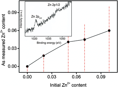 | ||
| Fig. 2 Zn2+ content of Sn1−xZnxWO4 nanocrystals measured by ICP-AES as a function of initial Zn2+ molar ratio. The inset shows the typical energy range related to Zn peaks. | ||
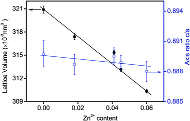 | ||
| Fig. 3 Lattice parameters of Sn1−xZnxWO4 (x = 0 to 0.060) nanocrystals as a function of dopant content of Zn2+. | ||
To characterize the structural and morphological properties, transmission electron microscopy (TEM) and high resolution TEM (HRTEM) were performed. Fig. 4a shows a typical TEM image of pure SnWO4 nanocrystals. It is seen that SnWO4 nanocrystals mainly consist of nanosheets with irregular shapes. For a single nanosheet, the spacing between adjacent lattice fringes was 0.155 nm (Fig. 4b), which is very close to that of 0.156 nm for the (121) plane as calculated by XRD, but slightly larger than that of 0.154 nm for SnWO4 (JCPDS card, No. 29-1354). However, after the incorporation of Zn2+ ions (x = 0.045), as shown in Fig. 4c, Sn1−xZnxWO4 nanocrystals were tuned to be rod-like tiny crystals with high crystallinity, as verified by the HRTEM image (Fig. 4d). Moreover, as the Zn2+ dopant concentration increased to 0.060, the Sn1−xZnxWO4 nanocrystals were entirely composed of nanowires with a diameter of ∼8 nm (inset of Fig. 4e) and a length of up to several hundreds of nanometers. The interplanar spacing of a single nanowire was about 0.154 nm (Fig. 4f), which is slightly smaller than that of the (121) plane for pure SnWO4 nanocrystals. It is noteworthy that the incorporation of Zn2+ ions into the SnWO4 host matrix led to dramatic changes in morphology. Knowledge of the shape evolution of the doped nanocrystals is still limited, although attempts to investigate the underlying mechanisms that control doping have been reported in the literature.11 For example, Wang et al. suggest that, for lanthanide-doped NaYF4 nanocrystals, the influence of lanthanide doping strongly depends on the size and dipole polarizability of the substitutional dopant ions.12 It is supposed that Zn dopants may play an important role in the primary growth stage and influence the intraparticle ripening process,11a which is critical for the generation of doped nanocrystals with different shapes.
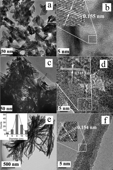 | ||
| Fig. 4 TEM and HRTEM images of pure SnWO4 (a, b), Sn1−xZnxWO4 (x = 0.045) (c, d) and Sn1−xZnxWO4 (x = 0.060) (e, f) nanocrystals. | ||
The energy level and the band gap of the oxide semiconductors play a crucial role in determining their photocatalytic activity. Fig. 5 shows optical band gap spectra of Sn1−xZnxWO4 (x = 0 to 0.060) nanocrystals as a function of Zn2+ dopant concentration. It is seen that all Sn1−xZnxWO4 nanocrystals exhibit a strong absorption band in the visible light region. According to previous literature, α-SnWO4 is a semiconductor with an indirect band gap.6a Thereby, the indirect band gap of Sn1−xZnxWO4 nanocrystals is estimated from the graph of hν versus (αhν)1/2 for the absorption coefficient α. The absorption coefficient α is related to the band gap Eg as
| αhv = A(hv − Eg)1/2 | (1) |
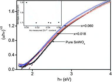 | ||
| Fig. 5 Optical band gap of Sn1−xZnxWO4 nanocrystals. | ||
What then is the reason for Zn2+ doped SnWO4 nanocrystals giving rise to the abnormal shift in the band gap energies? To answer this question, several factors should be taken into consideration, such as quantum size effect, lattice structure variations, electronic structure modifications, and surface structures. With regards to the quantum size effect, as stated above, all Sn1−xZnxWO4 nanocrystals have compatible particle sizes in the range 5.6 to 9.7 nm (calculated XRD results), which are in the region (i.e. <10 nm) for obvious quantum size effects.14 Therefore, the band gap energies of Sn1−xZnxWO4 nanocrystals are all larger than those of the bulk structure. However, for a particle size reduction by Zn2+ doping, we would expect a blue shift of the band gap energies, which contradicts the observed results. On the other hand, from the viewpoint of solid-state physics, the variation of lattice structures also has great impact on the static potential within the cells, which can have consequences for the electronic structures. As the neighboring atoms approach each other with lattice contraction of the solid, the basis functions overlap more strongly, producing increased dispersion of the electron bands in k space and consequently increased bandwidths along the energy axis.15 In other words, a blue shift of band gap energy is expected with a lattice contraction by Zn2+ doping.
To obtain further information on the electronic structures of the Sn1−xZnxWO4 nanocrystals, the density of states (DOS) was calculated on the basis of the plane-wave density function theory program package CASTEP. Fig. 6 displays the variation in DOS with energy. For pure SnWO4, as indicated in Fig. 6a, the top of the valence band maximum consists of O 2p, Sn 5s, and Sn 5p like orbitals due to the possibility of hybridization of Sn2+ with the O 2p orbitals, while the bottom of the conduction band minimum is predominantly composed of W 5d and Sn 5p states. Finally, the band gap energy of SnWO4 was calculated to be 1.65 eV. For Zn2+ doped in SnWO4 and substituted at the Sn2+ lattice site, the conduction band and valence band remain almost the same as those of pure SnWO4 (Fig. 6b). It is noted that the Zn 4s and Zn 4p orbitals show contributions to the top of the valence band and the bottom of the conduction band. Zn 3d orbitals mainly contribute to the middle of valence band (Fig. S3, ESI†). The band gap energy for Sn1−xZnxWO4 (x = 0.06) was calculated to be 1.63 eV, which is a bit smaller than that of pure SnWO4. This small red shift of the band gap energy could be attributed to the difference in electronegativity of the Zn2+ and Sn2+ ions. Till now, numerous works have been concentrated on the semiempirical correlation between optical band gap values of oxides and the difference in electronegativities of the elements.16 For binary oxides, the general relationship between the optical band gap of crystalline oxides and the difference in electronegativity of their constituents was suggested according to Phillips:17
 | (2) |
| Eg = 1.347 × (XM − XO)2 − 1.488 | (3) |
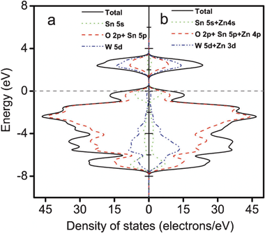 | ||
| Fig. 6 Density of states (DOS) of pure SnWO4 and Sn1−xZnxWO4 (x = 0.06). The horizontal dashed line represents the Fermi level. | ||
As for multi-metal oxides (i.e. BaTiO3, NaTaO3, La2Ti2O7),16b the electronegativity (XM) is replaced by the cationic group average electronegativity (![[X with combining macron]](https://www.rsc.org/images/entities/i_char_0058_0304.gif) c,a):
c,a):
 | (4) |
The impact of Zn2+ doping on the surface areas of SnWO4 nanocrystals was investigated using nitrogen adsorption and desorption isotherm curves. As shown in Fig. 7, the isotherm curves of pure and doped SnWO4 nanocrystals are characterized by a hybrid type between types I and IV in the Brunauer–Deming–Deming–Teller (BDDT) classification.19,20 The hysteresis loop resembles type B in de Boer's classification, which matches with the adsorbents with slit-shaped pores between the parallel layers. It is worth noting that the BET surface area of SnWO4 nanocrystals is only about 54 m2 g−1, which, however, increases to ∼100 m2 g−1 by Zn2+ doping (inset of Fig. 7). The alteration of surface area of the Sn1−xZnxWO4 nanocrystals predicts significantly enhanced photocatalytic activities.
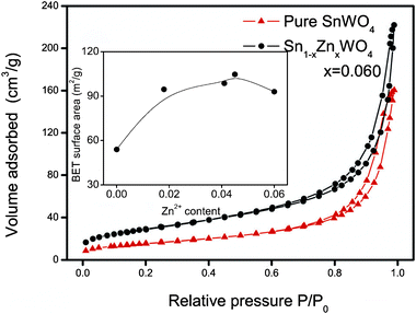 | ||
| Fig. 7 Nitrogen adsorption–desorption isotherms of Sn1−xZnxWO4 nanocrystals. The inset shows the BET surface area as a function of Zn2+ doping concentration. | ||
The photocatalytic activity of Sn1−xZnxWO4 nanocrystals was evaluated using methyl orange (MO) degradation as the model reaction. Temporal changes in the concentration of MO were monitored by examining the variations in maximal absorption in the UV-vis spectra at 464 nm. Fig. 8a shows the temporal evolution of the spectral changes of the MO mediated by Sn1−xZnxWO4 (x = 0.045). It can be found that the concentration of MO decreases quickly under visible light irradiation, and the peak (λ = 464 nm) nearly disappears after 25 min, while a new peak at 245 nm emerges, indicating that MO was degraded but was not completely mineralized in 25 min,2e which can also be verified by chemical oxygen demand (COD) data (Fig. S4, ESI†). Fig. 8b illustrates the photocatalytic activity for the degradation of MO under visible light irradiation over all Sn1−xZnxWO4 (x = 0–0.060) nanocrystals. It is clear to see that the photocatalytic performance of Sn1−xZnxWO4 nanocrystals can be flexibly tuned by Zn2+ doping. With the increase in Zn2+ doping concentration from 0 to 0.045, Sn1−xZnxWO4 nanocrystals showed greatly enhanced photocatalytic activity, while further increase in Zn2+ content led to an obvious decrease in photocatalytic performance.
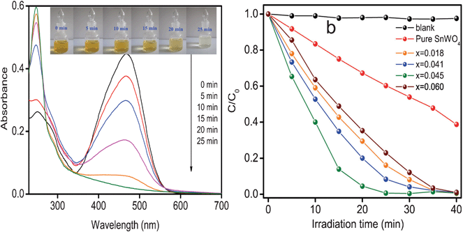 | ||
| Fig. 8 UV-vis spectral changes of MO in aqueous Sn1−xZnxWO4 (x = 0.045) dispersion as a function of irradiation time (a) and normalized concentration of methyl orange versus visible light irradiation time in the presence of Sn1−xZnxWO4 nanocrystals at various Zn2+ doping concentrations (b). | ||
Generally, when a semiconductor absorbs a photon with energy greater than or equal to the band gap energy, an electron would be promoted from the valence band to the conduction band, leaving a hole in the valence band. If this charge separation is valid, these electrons and holes could migrate to the surface of the semiconductor to react with the adsorbed O2 and H2O, respectively, in producing the redox sources of the O2−· and OH· radical species, which lead to the efficient destruction of organic pollutants.21 On the basis of UV-visible and DFT results, one can see that all Sn1−xZnxWO4 nanocrystals have a narrow band gap in the visible region. In order to fully understand the effect of the electronic structure characteristics on the photocatalytic activity, the band edge positions of the valence band (VB) and conduction band (CB) of the Sn1−xZnxWO4 nanocrystals were determined because they are also strongly related to the process of photocatalytic oxidation of organic compounds. Although the band edge positions are not easily determined experimentally, a theoretical prediction is possible using concepts of Mulliken electronegativity. The conduction band edge energy of a semiconductor at the point of zero charge can be expressed by22
| ECB = X − Ee − 0.5Eg | (5) |
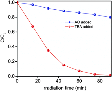 | ||
| Fig. 9 Photocatalytic degradation of MO in the presence of ammonium oxalate (AO, scavenger for holes) or tert-butyl alcohol (TBA, scavenger for OH· radical species) under visible irradiation over Sn1−xZnxWO4 (x = 0.045) nanocrystals. | ||
As for the enhancement of the photocatalytic activities of Sn1−xZnxWO4 nanocrystals, several factors should be taken into consideration. (1) BET surface area may impose a great impact on the photocatalytic activity of the nanocrystals. The majority of photocatalytic reactions occur at semiconductor surfaces, and therefore the photocatalytic activities of semiconductor oxides are usually greatly improved by the increase in surface area.29 For the present Sn1−xZnxWO4 nanocrystals, the BET surface area is ∼54 m2 g−1, which, however, greatly increases to ∼100 m2 g−1 with Zn2+ doping. The increase in surface area will improve the surface active sites and photonic efficiency, which favors an increased ratio of surface charge carrier transfer rate to electron–hole recombination rate. (2) Doping effects may have a great influence on the charge carriers and the subsequent photocatalytic activity. Doping with transition metal ions including V, Fe, Co, and Cu has shown both positive and negative effects on the photocatalytic activity.3a–c,30 For instance, Choi et al. reported that the photocatalytic activity of transition metal ion doped TiO2 increases as the dopant concentration is increased, but that there exists a complex dependence on dopant concentration, dopant energy state in the lattice, d-electron configuration, distribution of dopants, and electron donor concentration.4a On the basis of the XRD and DFT calculation results, Zn2+ ions were homogeneously incorporated into SnWO4, leading to the hybridization of the W 5d and Zn 3d orbitals, which may increase the mobility of photogenerated charge carriers in the valence band, and subsequently enhance the photocatalytic activity. On the other hand, Zn2+ ions with higher doping concentrations may also serve as a recombination center for electrons and holes, thus diminishing the overall photocatalytic activity of Sn1−xZnxWO4 nanocrystals. Considering the BET surface area and doping effects, Sn1−xZnxWO4 nanocrystals showed an optimized photocatalytic activity at a Zn2+ doping level of x = 0.045.
Conclusion
Sn1−xZnxWO4 nanocrystals were successfully prepared via a microwave-assisted hydrothermal approach. The homogeneous incorporation of Zn2+ ions into the SnWO4 host lattice led to a monotonous lattice contraction. The solubility of Zn2+ in SnWO4 was measured to be about 0.060 by chemical analyses. One notable result of this work is the demonstration that, by Zn2+ doping, SnWO4 nanocrystals can be controlled to achieve morphological alteration, enlarged BET surface area, band gap narrowing and highly enhanced photocatalytic performance. With well-controlled morphology, surface area, and electronic structure via Zn2+ doping, the photocatalytic performance of Sn1−xZnxWO4 nanocrystals was optimized at a Zn2+ doping level of x = 0.045. Such a finding is fundamentally important, and may help to provide hints for developing and designing new photocatalytic semiconductors.Acknowledgements
This work is financially supported by the National Natural Science Foundation of China (Grants 21103081, 51102129 and 20967004), the Program of Higher-Level Talents of Inner Mongolia University (Grant Z20090106), the Project of Scientific and Technological Innovation Team of Inner Mongolia University (12110614).References
- (a) D. J. Norris, A. L. Efros and S. C. Erwin, Science, 2008, 319, 1776 CrossRef CAS; (b) Y. F. Yang, Y. Z. Jin, H. P. He, Q. L. Wang, Y. Tu, H. M. Lu and Z. Z. Ye, J. Am Chem. Soc, 2010, 132, 12281 Search PubMed; (c) X. Q. Qiu, L. P. Li, J. Zheng, J. J. Liu, X. F. Sun and G. S. Li, J. Phys. Chem. C, 2008, 112, 12242 CrossRef CAS; (d) J. W. Qin, M. H. Cao, N. Li and C. W. Hu, J. Mater. Chem., 2011, 21, 17167 RSC.
- (a) C. T. Ho, K. B. Low, P. Jash, H. Y. Shen, P. T. Snee and R. J. Meyer, Chem. Mater., 2011, 23, 4721 CrossRef CAS; (b) T. L. Tompson and J. T. Y. Yates Jr., Chem. Rev., 2006, 106, 4428 CrossRef; (c) A. B. Jorge, Y. Sakatani, C. Boissiere, C. Laberty-Roberts, G. Sauthier, J. Fraxedas, C. Sanchez and A. Fuertes, J. Mater. Chem., 2012, 22, 3220 RSC; (d) Z. Z. Zhang, X. X. Wang, J. L. Long, Q. Gu, Z. X. Ding and X. Z. Fu, J. Catal., 2010, 276, 201 CrossRef CAS; (e) M. Sun, D. Z. Li, W. J. Li, Y. B. Chen, Y. H. He and X. Z. Fu, J. Phys. Chem. C, 2008, 112, 18076 CrossRef CAS.
- (a) S. Bingham and W. A. Daoud, J. Mater. Chem., 2011, 21, 2041 RSC; (b) Q. Xiao, J. Zhang, C. Xiao and X. K. Tan, Mater. Sci. Eng., B, 2007, 142, 121 CrossRef CAS; (c) G. Colon, M. Maicu, M. C. Hidalgo and J. A. Navio, Appl. Catal., B, 2006, 67, 41 CrossRef CAS; (d) H. Kato, K. Asakura and A. Kudo, J. Am. Chem. Soc., 2003, 125, 3082 CrossRef CAS.
- (a) W. Y. Choi, A. Termin and M. R. Hoffmann, J. Phys. Chem., 1994, 98, 13669 CrossRef; (b) H. F. Shi, Z. S. Li, J. H. Kou, J. H. Ye and Z. G. Zou, J. Phys. Chem. C, 2011, 115, 145 CrossRef CAS.
- D. F. Wang, J. H. Ye, T. Kako and T. Kimura, J. Phys. Chem. B, 2006, 110, 15824 CrossRef CAS.
- (a) I. S. Cho, C. H. Kwak, D. W. Kim, S. Lee and K. S. Hong, J. Phys. Chem. C, 2009, 113, 10647 CrossRef CAS; (b) A. Mukherji, B. Seger, G. Q. Lu and L. Z. Wang, ACS Nano, 2011, 5, 3483 CrossRef CAS; (c) M. Sun, D. Z. Li, W. J. Zhang, Z. X. Chen, H. J. Huang, W. J. Li, Y. H. He and X. Z. Fu, J. Phys. Chem. C, 2009, 113, 14916 CrossRef CAS.
- B. Panigrahy, M. Aslam and D. Bahadur, J. Phys. Chem. C, 2010, 114, 11758 CAS.
- H. Dong, Z. H. Li, Z. X. Ding, H. B. Pan, X. X. Wang and X. Z. Fu, Sens. Actuators, B, 2009, 140, 623 CrossRef.
- S. F. Matar, G. Campet and M. A. Subramanian, Prog. Solid State Chem., 2011, 39, 70 CrossRef CAS.
- W. B. Hu, W. M. Tong, L. P. Li, J. Zheng and G. S. Li, Phys. Chem. Chem. Phys., 2011, 13, 11634 RSC.
- (a) L. J. Zhu, D. J. Norris, T. A. Kennedy, S. C. Erwin and A. L. Efros, Nano Lett., 2006, 6, 334 CrossRef; (b) N. Qiu, J. Zhang, Z. Y. Wu, T. D. Hu and P. Liu, Cryst. Growth Des., 2012, 12, 629 CrossRef CAS.
- F. Wang, Y. Han, C. S. Lim, Y. H. Lu, J. Wang, J. Xu, H. Y. Chen, C. Zhang, M. H Hong and X. G. Liu, Nature, 2010, 463, 1061 CrossRef CAS.
- (a) X. B. Chen and C. Burda, J. Am. Chem. Soc., 2008, 130, 5018 CrossRef CAS; (b) H. G. Yu, H. Irie and K. Hashimoto, J. Am. Chem. Soc., 2010, 132, 6898 CrossRef CAS.
- A. C. Yanes, J. D. Castillo, M. Torres and J. Peraza, Appl. Phys. Lett., 2004, 85, 2343 CrossRef CAS.
- Ü. Özgür, Y. I. Alivov, C. Liu, A. Teke, M. A. Reshchikov, S. Doğan, V. Avrutin, S. J. Cho and H. Morkoç, J. Appl. Phys., 2005, 98, 041301 CrossRef.
- (a) R. R. Reddy, K. R. Gopal, K. Narasimhulu, L. S. S. Reddy, K. R. Kumar, C. V. K. Reddy and S. N. Ahmed, Opt. Mater., 2008, 31, 209 CrossRef CAS; (b) F. D. Quarto, C. Sunseri, S. Piazza and M. C. Romano, J. Phys. Chem. B, 1997, 101, 2519 CrossRef.
- J. C. Phillips, Bonds and Bands in Semiconductors, Academic Press, New York, London, 1973 Search PubMed.
- M. Lannoo and L. Bourgoin, Point Defects in Semiconductors I, Berlin, Springer 1981, ch. 2,3 Search PubMed.
- S. J. Gregg and K. S. W. Sing, Adsorption, Surface Area, and Porosity, Academic Press, London, 2nd edn, 1983 Search PubMed.
- T. Allen, Particle Size Measurement, Chapman and Hall, London, 4th edn, 1980, p. 20 Search PubMed.
- (a) L. S. Roselin, G. R. Rajarajeswari, R. Selvin, V. Sadasivam, B. Sivasankar and K. Rengaraj, Sol. Energy, 2002, 73, 281 CrossRef CAS; (b) M. J. Height, S. E. Pratsinis, O. Mekasuwandumrong and P. Praserthdam, Appl. Catal., B, 2006, 63, 305 CrossRef CAS.
- (a) A. H. Nethercot, Phys. Rev. Lett., 1974, 33, 1088 CrossRef CAS; (b) M. A. Butler and D. S. Ginley, J. Electrochem. Soc., 1978, 125, 228 CrossRef CAS.
- J. W. Tang and J. H. Ye, Chem. Phys. Lett., 2005, 410, 104 CrossRef CAS.
- G. C. Xiao, X. C. Wang, D. Z. Li and X. Z. Fu, J. Photochem. Photobiol., A, 2008, 193, 213 CrossRef CAS.
- A. J. Bard, R. Parsons and J. Jordan, Standard Potentials in Aqueous Solution, Marcel Dekker, New York and Basel, 1985 Search PubMed.
- A. Fujishima, T. N. Rao and D. A. Tryk, J. Photochem. Photobiol., C, 2000, 1, 1 CrossRef CAS.
- O. Carp, C. L. Huisman and A. Reller, Prog. Solid State Chem., 2004, 32, 33 CrossRef CAS.
- A. A. Khodja, T. Sehili, J. F. Pilichowski and P. Boule, J. Photochem. Photobiol., A, 2001, 141, 231 CrossRef CAS.
- L. P. Li, J. J. Liu, Y. G. Su, G. S. Li, X. B. Chen, X. Q. Qiu and T. J. Yan, Nanotechnology, 2009, 20, 155706 CrossRef.
- S. Klosek and D. Raftery, J. Phys. Chem. B, 2001, 105, 2815 CrossRef CAS.
Footnote |
| † Electronic Supplementary Information (ESI) available: Figures showing XPS spectra of Sn1−xZnxWO4 nanocrystals and density of states (DOS) of Zn in Sn1−xZnxWO4. See DOI: 10.1039/c2ra20401k/ |
| This journal is © The Royal Society of Chemistry 2012 |